

SGS Thomson Microelectronics STP12PF06 Datasheet
STP12PF06
P - CHANNEL 60V - 0.18 Ω - 12A TO-220
STripFET POWER MOSFET
TYPE V
DSS
R
DS(o n)
I
D
ST P12PF06 60 V < 0. 20 Ω 12 A
■ TYPICALR
■ EXCEPTIONALdv/dt CAPABILITY
■ 100%AVALANCHETESTED
■ LOW GATE CHARGE
■ APPLICATIONORIENTED
DS(on)
= 0.18 Ω
CHARACTERIZATIONL
DESCRIPTION
This Power MOSFET is the latest developmentof
STMicroelectronics unique ”Single Feature
Size” strip-based process. The resulting transi-
stor shows extremely high packing density for low
on-resistance, rugged avalanche characteristics
and less critical alignment steps therefore a remarkablemanufacturingreproducibility.
APPLICATIONS
■ MOTORCONTROL
■ DC-DC& DC-AC CONVERTERS
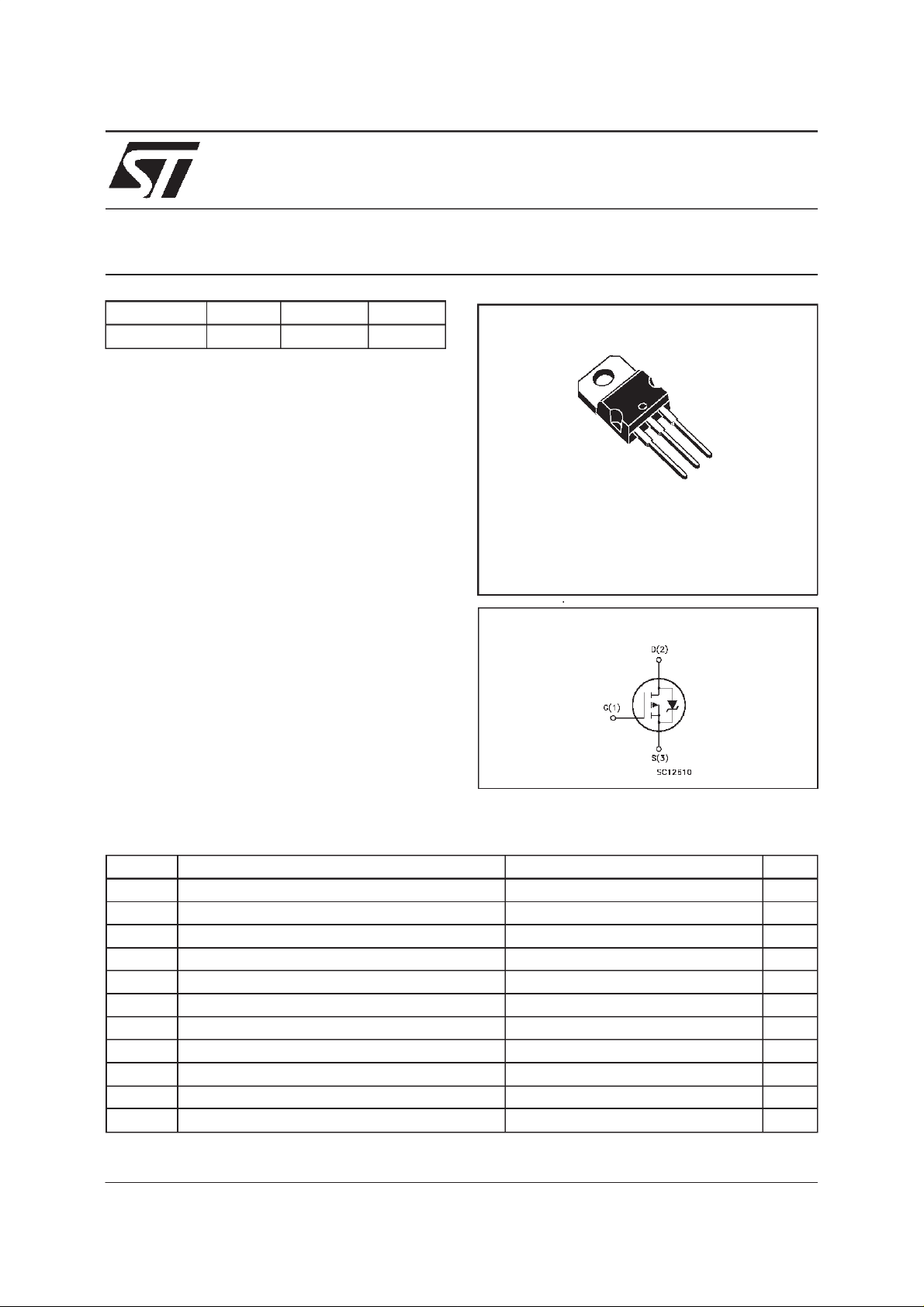
3
2
1
TO-220
INTERNAL SCHEMATIC DIAGRAM
ABSOLUTE MAXIMUM RATINGS
Symbol Parameter Value Uni t
V
V
V
I
DM
P
dv/ d t Peak Diode Recover y volta ge s lope 6 V / ns
T
(•) Pulse width limited by safe operating area (1)I
Note:For the P-CHANNEL MOSFET actual polarity of voltages and current has to be reversed
May 2000
Drain-source Voltage (VGS=0) 60 V
DS
Drain- gat e Volt age (RGS=20kΩ)60V
DGR
Gate-source Voltage
GS
I
Drain Current (cont inuous) at Tc=25oC12A
D
I
Drain Current (cont inuous) at Tc=100oC8.4A
D
20 V
±
(•) Drain Current (pulsed) 48 A
Total Dissipation at Tc=25oC60W
tot
Derat ing Fac tor 0.4 W/
Sto rage T emperature -65 t o 175
stg
T
Max. Opera ti ng Junction Tempe r at ure 175
j
≤
12 A, di/dt≤300A/µs, V
SD
DD
≤
V
(BR)DSS,Tj
≤
T
JMAX
o
C
o
C
o
C
1/8
STP12PF06
THERMAL DATA
R
thj-case
R
thj-amb
R
thc-sink
T
AVALANCHE CHARACTERISTICS
Symbol Parameter Max Value Unit
I
AR
E
Ther mal Resistanc e Junct ion-case Max
Ther mal Resistanc e Junct ion-ambient Max
Ther mal Resistanc e Case-sink Ty p
Maximum Lead Te m perature For So lder ing Purpos e
l
Avalanche Current, Repetitive or Not-Repetitive
(pulse width limited by T
Single Pulse A valanche E ner gy
AS
(starting T
=25oC, ID=IAR,VDD=25V)
j
max)
j
2.5
62.5
0.5
275
12 A
200 mJ
o
C/W
o
C/W
o
C/W
o
C
ELECTRICAL CHARACTERISTICS
=25oC unless otherwisespecified)
(T
case
OFF
Symbol Parameter Test Condit ions Min. Typ. M ax. Unit
V
(BR)DSS
Drain-source
ID=250µAVGS=0 60 V
Break dow n Volt age
I
DSS
I
GSS
Zero Gate Voltage
Drain Current (V
GS
Gat e- bod y Leakag e
Current (V
DS
=0)
=0)
V
=MaxRating
DS
=MaxRating Tc= 125oC
V
DS
V
=± 20 V
GS
1
10
100 nA
±
ON(∗)
Symbol Parameter Test Condit ions Min. Typ. M ax. Unit
V
GS(th)
R
DS(on)
Gate Threshold Voltage VDS=VGSID= 250 µA23.44V
Sta t ic Dr ain -s ource O n
VGS=10V ID= 6 A 0.18 0.20
Resistance
I
D(on)
On State Drain Current VDS>I
D(on)xRDS(on )max
12 A
VGS=10V
DYNAMIC
Symbol Parameter Test Condit ions Min. Typ. M ax. Unit
g
(∗)Forward
fs
Tr ansc on duc tance
C
C
C
Input C apac i t ance
iss
Out put Capacit ance
oss
Reverse T r ansfer
rss
Capacit a nc e
VDS>I
D(on)xRDS(on )maxID
=6A 2.5 6 S
VDS=25V f=1MHz VGS= 0 850
230
75
µ
µA
Ω
pF
pF
pF
A
2/8
STP12PF06
ELECTRICAL CHARACTERISTICS
(continued)
SWITCHINGON
Symbol Parameter Test Condit ions Min. Typ. M ax. Unit
t
d(on)
Tur n-on Delay T ime
Rise T i me
t
r
VDD=30V ID=6A
R
=4.7
G
Ω
VGS=10V
20
40
(Resis t iv e Load, see f ig. 3)
Q
Q
Q
Tot al G at e Char ge
g
Gat e- Source Charge
gs
Gate-Drain Charge
gd
VDD=48V ID=12A VGS=10V 16
4
6
21 nC
SWITCHINGOFF
Symbol Parameter Test Condit ions Min. Typ. M ax. Unit
t
d(off)
Tur n-of f Delay Time
t
Fall T ime
f
VDD=30V ID=6A
=4.7 Ω VGS=10V
R
G
40
10
(Resis t iv e Load, see f ig. 3)
t
r(Voff)
t
t
Off-volt ag e Rise Time
Fall T ime
f
Cross-over Time
c
VDD=48V ID=12A
=4.7 Ω VGS=10V
R
G
(Indu ct iv e L oad , see fig . 5)
10
17
30
SOURCEDRAINDIODE
Symbol Parameter Test Condit ions Min. Typ. M ax. Unit
I
V
I
SDM
SD
Q
I
RRM
SD
t
Source-drain Current
(•)
Source-drain Current
10
40
(pulsed)
(∗)ForwardOnVoltage ISD=12A VGS=0 2.5 V
Reverse Re covery
rr
Time
Reverse Re covery
rr
ISD= 12 A di/dt = 100 A /µs
=30V Tj=150oC
V
DD
(see test circuit, fig. 5)
100
260
Charge
Reverse Re covery
5.2
Current
ns
ns
nC
nC
ns
ns
ns
ns
ns
A
A
ns
nC
A
(∗) Pulsed: Pulse duration = 300 µs, duty cycle 1.5 %
(•) Pulse width limited by safe operating area
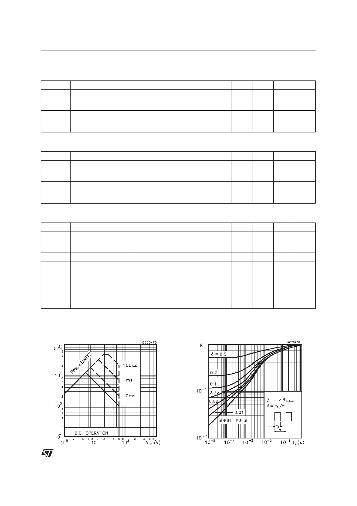
SafeOperating Area ThermalImpedance
3/8
 Loading...