

SGS Thomson Microelectronics STP12NM50FP, STP12NM50, STB12NM50-1 Datasheet
STP12NM50 - STP12NM50FP
STB12NM50-1
N-CHANNEL 500V - 0.3Ω - 12A TO-220/TO-220FP
TYPE V
STP12NM50/FP 500V <0.35Ω 12 A
STB12NM50-1 500V <0.35Ω 12 A
■ TYPICAL R
■ HIGH dv/dt ANDAVALANCHE CAPABILITIES
■ 100% AVALANCHE TESTED
■ LOW INPUT CAPACITANCE AND GATE CHARGE
■ LOW GATE INPUT RESISTANCE
■ TIGHT PROCESS CONTROL AND HIGH
DS
DSS
(on) = 0.3Ω
MANUFACTURING YIELDS
DESCRIPTION
The MDmesh is a new revolutionary MOSFET technology that associates the Multiple Drain process with
the Company’sPowerMESH horizontal layout. The
resulting product has an outstanding low on-resistance, impressively high dv/dt andexcellent avalanche
characteristics. The adoption of the Company’s proprietary strip technique yields overall dynamic performance that is significantly better than that of similar
competition’s products.
R
DS(on)
I
D
/I
PAK
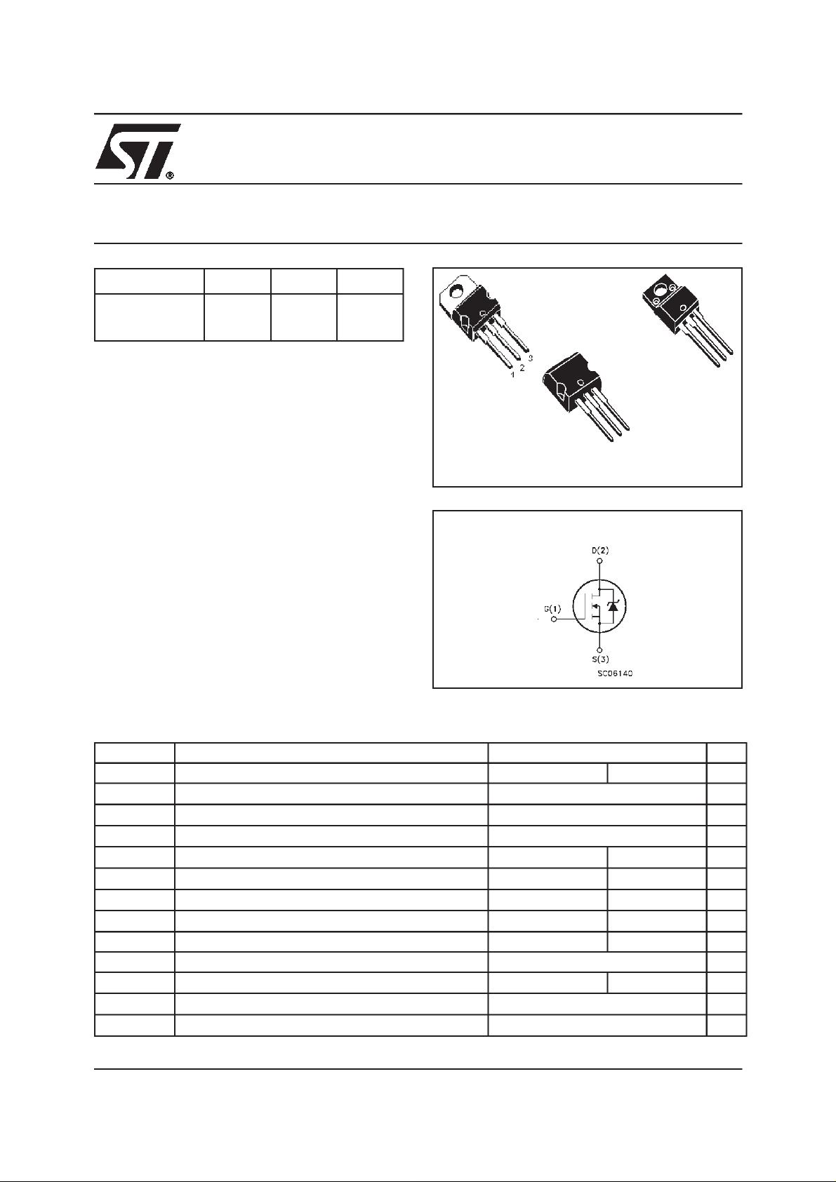
MDmeshPower MOSFET
TO-220
2
1
I PAK
(Tabless TO-220)
INTERNAL SCHEMATIC DIAGRAM
TO-220FP
3
1
3
2
APPLICATIONS
The MDmesh family is very suitable for increasing
power density of high voltage converters allowing system miniaturization and higher efficiencies.
ABSOLUTE MAXIMUM RATINGS
Symbol Parameter Value Unit
STP(B)12NM50(-1) STP12NM50FP
V
DS
V
DGR
V
GS
I
D
I
D
I
DM
P
TOT
dv/dt(1) Peak Diode Recovery voltage slope 6 V/ns
V
ISO
T
stg
T
(•)Pulse width limitedby safe operating area
This is preliminary information ona new product now in development or undergoing evaluation. Details are subject to change without notice.
Drain-source Voltage (VGS=0)
Drain-gate Voltage (RGS=20kΩ)
Gate- source Voltage ±30 V
Drain Current (continuos) at TC=25°C
Drain Current (continuos) at TC= 100°C
(●)
Drain Current (pulsed) 48 48(*) A
TotalDissipation at TC=25°C
Derating Factor 0.88 0.28 W/°C
Insulation Winthstand Voltage (DC) -- 2000 V
Storage Temperature –65 to 150 °C
Max. Operating Junction Temperature 150 °C
j
(1)ISD≤12A, di/dt ≤200A/µs, VDD≤ V
(*)Limited only by maximum temperature allowed
12 12(*) A
7.5 7.5(*) A
110 35 W
500 V
500 V
(BR)DSS,Tj≤TJMAX.
1/10April 2000
STP12NM50/FP/STB12NM50-1
THERMAL DATA
TO-220 / I PAK TO-220FP
Rthj-case Thermal Resistance Junction-c ase Max 1.13 3.57 °C/W
Rthj-amb Thermal Resistance Junction-ambient Max 62.5 °C/W
Rthc-sink Thermal Resistance Case-sink Typ 0.5 °C/W
T
l
AVALANCHE CHARACTERISTICS
Symbol Parameter Max Value Unit
I
AR
E
AS
ELECTRICAL CHARACTERISTICS (TCASE = 25 °C UNLESS OTHERWISE SPECIFIED)
OFF
Symbol Parameter Test Con ditions Min. Typ. Max. Unit
V
(BR)DSS
I
DSS
I
GSS
Maximum Lead Temperature For Soldering P urpose 300 °C
Avalanche Current, Repetitive or Not-Repetitiv e
(pulse width limited by T
max)
j
Single Pu lse Avala nche Energy
(starting T
Drain-source
Breakdown Voltage
Zero Gate Voltage
Drain Current (V
Gate-body Leakage
Current (V
=25°C, ID=IAR,VDD=50V)
j
I
= 250 µ A, VGS=0
D
= Max R ating
V
DS
=0)
DS
GS
=0)
V
= Max R ating, TC= 125 ° C
DS
= ±30V
V
GS
500 V
12 A
400 mJ
1 µA
10 µA
±100 nA
ON (1)
Symbol Parameter Test Con ditions Min. Typ. Max. Unit
V
GS(th)
R
DS(on)
I
D(on)
Gate Thre shold Voltage
Static Drain-source On
Resistance
On State Drain Current
V
DS=VGS,ID
V
= 10V, ID=6A
GS
V
DS>ID(on)xRDS(on)max,
= 250µA
VGS=10V
345V
0.3 0.35 Ω
12 A
DYNAMIC
Symbol Parameter Test Con ditions Min. Typ. Max. Unit
V
(1)
g
fs
C
iss
C
oss
C
rss
R
g
Note: 1. Pulsed: Pulse duration = 300 µs, duty cycle 1.5 %.
Forward Transconductance
Input Capacitance
Output Capacitance 180 pF
Reverse Transfer
Capacitance
Gate Input Resistance
DS>ID(on)xRDS(on)max,
ID=6A
V
= 25V, f = 1 MHz, VGS=0
DS
f=1 MHz G ate DC Bias=0
Test Signal Level=20mV
Open D rain
5.2 S
1000 pF
25 pF
1.6 Ω
2/10
STP12NM50/FP/STB12NM50-1
ELECTRICAL CHARACTERISTICS (CONTINUED)
SWITCHING ON
Symbol Parameter Test Conditions Min. Typ. Max. Unit
t
d(on)
Q
Q
Q
t
r
g
gs
gd
Turn-on Delay Time
Rise Time 10 ns
TotalGate Charge
Gate-Source Charge 8 nC
Gate-Drain Charge 15 nC
SWITCHING OFF
Symbol Parameter Test Conditions Min. Typ. Max. Unit
t
r(Voff)
t
t
f
c
Off-voltage Rise Time
Fall Time 8 ns
Cross-over Time 18 ns
SOURCE DRAIN DIODE
Symbol Parameter Test Conditions Min. Typ. Max. Unit
I
SD
I
SDM
V
SD
t
rr
Q
rr
I
RRM
Note: 1. Pulsed: Pulse duration = 300 µs, duty cycle 1.5 %.
2. Pulse width limited by safe operating area.
Source-drain Current 12 A
(2)
Source-drain Current (pulsed) 48 A
(1)
Forward On Voltage
Reverse Recovery Time
Reverse Recovery Charge 5.25 µC
Reverse Recovery Current 30 A
V
= 250V, ID=6A
DD
= 4.7Ω VGS= 10V
R
G
(see test circuit, Figure 3)
V
= 400V, ID= 12A,
DD
= 10V
V
GS
V
= 400V, ID=12A,
DD
=4.7Ω, VGS= 10V
R
G
(see test circuit, Figure 5)
ISD=12A,VGS=0
I
= 12 A, di/dt = 100A/µs,
SD
= 100V, Tj= 150°C
V
DD
(see test circuit, Figure 5)
20 ns
28 nC
19 ns
1.5 V
350 ns
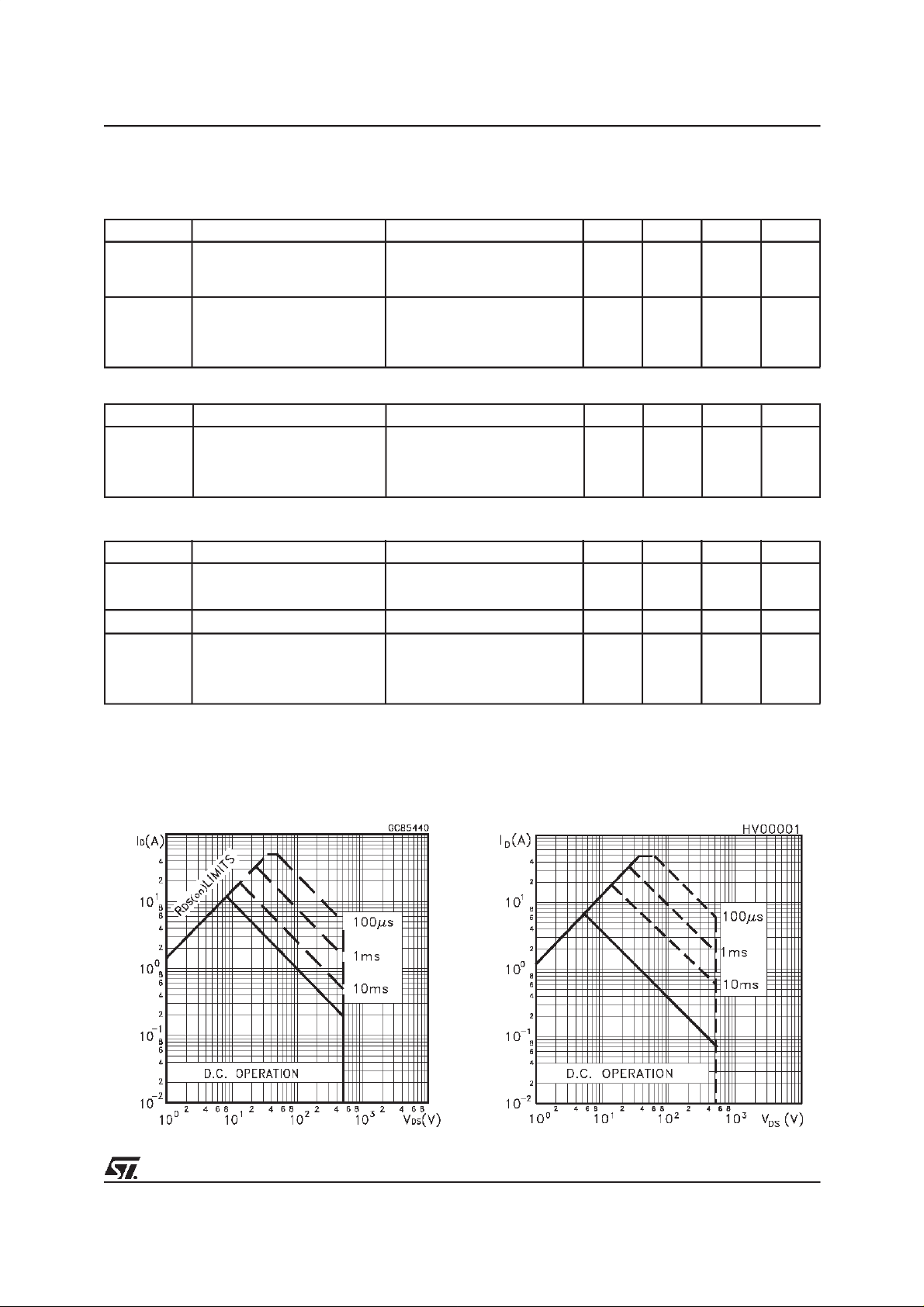
Safe Operating Area For TO-220 / I P AK Safe Operating Area For TO-220FP
3/10
 Loading...