

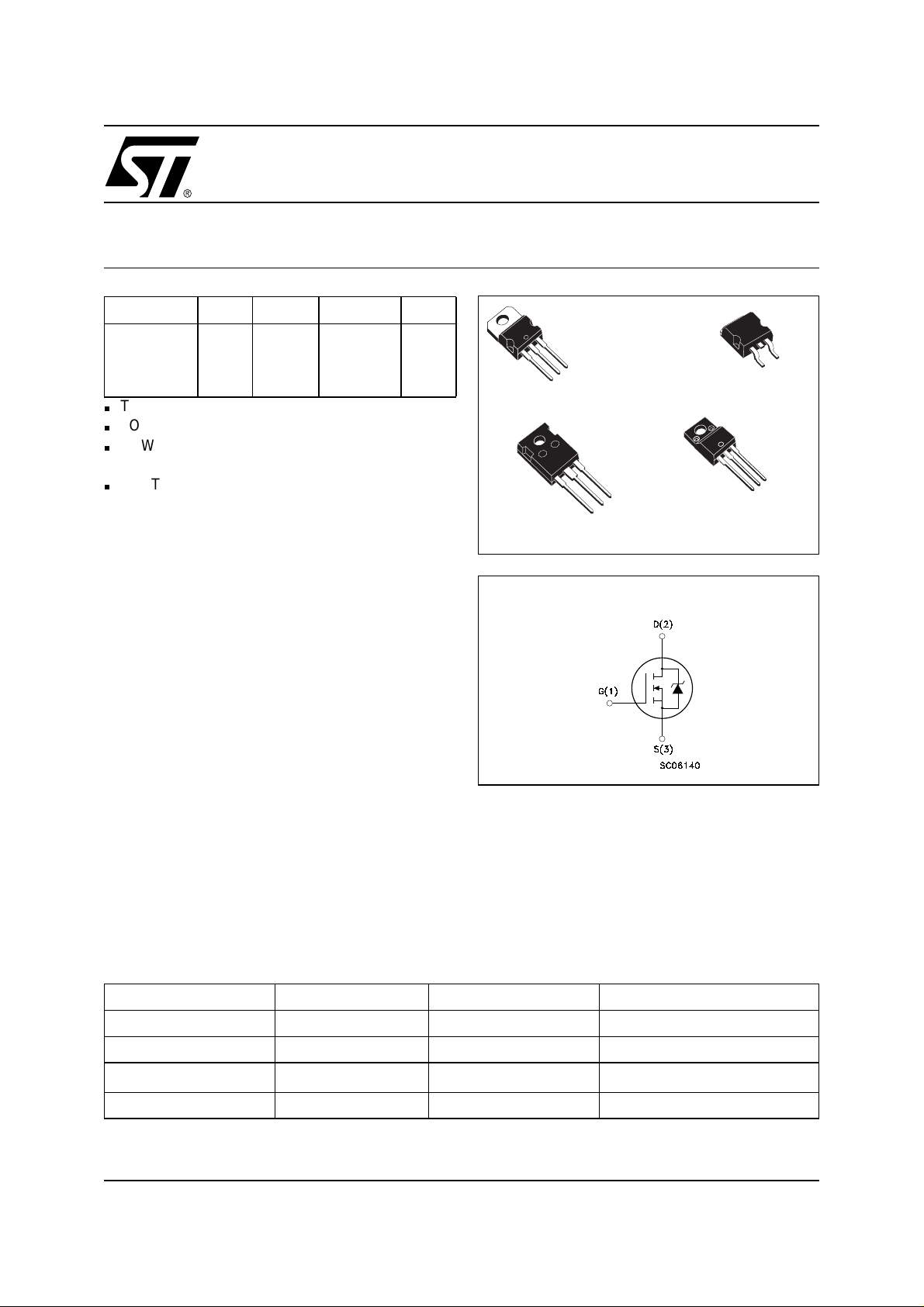
STP11NM80 - STB11NM80
STF11NM80 - STW11NM80
N-CHANNEL 800V - 0.35Ω - 11A TO-220/FP/D2PAK/TO-247
MDmesh™Power MOSFET
TARGET DATA
TYPE V
STP11NM80
STF11NM80
STB11NM80
STW11NM80
TYPICAL RDS(on) = 0.35 Ω
LOW GATE INPUT RESISTANCE
LOW INPUT CAPACITANCE AND GATE
800 V
800 V
800 V
800 V
DSS
R
DS(on)Rds(on)*Qg
< 0.40 Ω
< 0.40 Ω
< 0.40 Ω
< 0.40 Ω
14 Ω*nC
14 Ω*nC
14 Ω*nC
14 Ω*nC
I
D
11 A
11 A
11 A
11 A
CHARGE
BEST R
* Qg IN THE INDUSTRY
ds(on)
DESCRIPTION
The MDmesh™ is a new revolutionary MOSFET
technology that associates the Multiple Drain process with the Company’s PowerMESH™ horizontal
layout. The resulting product has an outstanding low
on-resistance, impressively high dv/dt and excellent
avalanche characteristics. The adoption of the
Company’s proprietary strip technique yields overall
dynamic performance that is significantly better than
that of similar competition’s products.
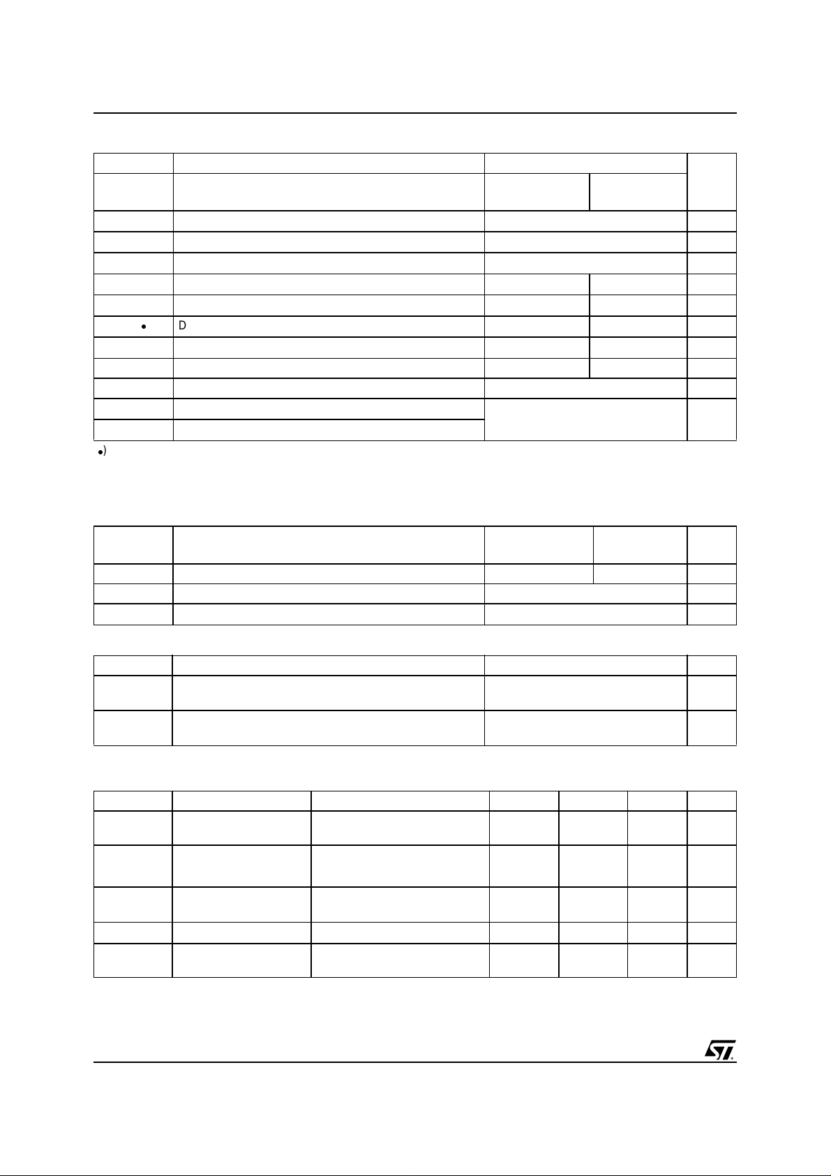
3
2
1
D2PAK
TO-220
3
2
1
TO-220FP
TO-247
INTERNAL SCHE MATIC DIAGRAM
3
1
3
2
1
APPLICATIONS
The 800 V MDmes h™ family is very su itable for single switch applications in particular for Flyback and
Forward converter topologies.
ORDERING INFORMATION
SALES TYPE MARKING PACKAGE PACKAGING
STP11NM80 P11NM80 TO-220 TUBE
STF11NM80 F11NM80 TO-220FP TUBE
STB11NM80T4 B11NM80
STW11NM80 W11NM80 TO-247 TUBE
June 2003
2
PAK
D
TAPE & REEL
1/10
STP11NM80 - ST B 11NM 80 - S TF11NM 80 - STW11NM 80
ABSOLUTE M AXIMUM RATINGS
Symbol Parameter Value Unit
TO-220/D
Drain-source Voltage (VGS=0)
Drain-gate Voltage (RGS=20kΩ)
Gate- source Voltage ± 30 V
Drain Current (continuous) at TC= 25°C
Drain Current (continuous) at TC= 100°C
()
Drain Current (pulsed) 44 44 (*) A
Total Dissipation at TC= 25°C
I
V
DM
P
V
DGR
V
I
I
TOT
DS
GS
D
D
Derating Factor 1.2 0.28 W/°C
dv/dt(1) Peak Diode Recovery voltage slope 15 V/ns
T
stg
T
j
Storage Temperature
Max. Operating Junction Temperature
()Pulse width limited by safe operating area
<11A, di/dt<400A/µs, VDD<V
(1)I
SD
(*) Limited only by the Maximum Temperature Allowed
(BR)DSS,TJ<TJMAX
2
PAK
TO-247
TO-220FP
800 V
800 V
11 11 (*) A
4.7 4.7 (*) A
150 35 W
–65 to 150 °C
THERMAL DATA
2
TO-247
PAK
TO-220FP
TO-220/D
Rthj-case Thermal Resistance Junction-case Max 0.83 3.6 °C/W
Rthj-amb Thermal Resistance Junction-ambient Max 62.5 °C/W
T
l
Maximum Lead Temperature For Soldering Purpose 300 °C
AVALANCHE CHARACTERISTICS
Symbol Parameter Max Value Unit
I
AR
E
AS
Avalanche Current, Repetitive or Not-Repetitive
(pulse width limited by T
max)
j
Single Pulse Avalanche Energy
(starting T
= 25 °C, ID= 2.5A, VDD=50V)
j
ELECTRICAL CHARACT ERISTICS (T
= 25 °C UNLESS OTHERWISE SPECIFIED)
CASE
TBD A
TBD mJ
ON/OFF
Symbol Parameter Test Conditions Min. Typ. Max. Unit
V
(BR)DSS
I
DSS
I
GSS
V
GS(th)
R
DS(on)
Drain-source
Breakdown Voltage
Zero Gate Voltage
Drain Current (V
GS
Gate-body Leakage
Current (V
DS
=0)
Gate Threshold Voltage
Static Drain-source On
Resistance
ID= 250 µA, VGS= 0 800 V
V
= Max Rating
DS
=0)
VDS= Max Rating, TC=125°C
V
= ±30V 100 nA
GS
V
DS=VGS,ID
= 250 µA 3
4
VGS=10V,ID= 5.5 A 0.35 0.40 Ω
10 µA
100 µA
5V
2/10
STP11NM80 - STB11NM80 - STF11NM80 - STW11NM80
ELECTRICAL CHARACT ERISTICS (CO NTINUED)
DYNAMIC
Symbol Parameter Test Conditions Min. Typ. Max. Unit
(1) Forward Transconductance VDS>I
g
fs
D(on)xRDS(on)max,
ID= 7.5 A
V
C
iss
C
oss
C
rss
Input Capacitance
Output Capacitance 1000 pF
Reverse Transfer
=30V,f=1MHz,VGS=0
DS
Capacitance
R
G
Gate Input Resistance f=1 MHz Gate DC Bias = 0
Test Signal Level = 20mV
Open Drain
(1)Pulsed: Pulse duration = 300 µs, duty cycle 1.5 %.
SWITCHING ON
Symbol Parameter Test Conditions Min. Typ. Max. Unit
V
t
d(on)
Q
Q
Q
Turn-on Delay Time
t
r
g
gs
gd
Rise Time 14 ns
Total Gate Charge
Gate-Source Charge 10 nC
Gate-Drain Charge 24 nC
=400V,ID= 5.5 A
DD
R
= 4.7 Ω ,VGS= 10V
G
(see test circuit, Figure 3)
V
=400V,ID=11A,
DD
VGS=10V
5S
1900 pF
18 pF
2 Ω
27 ns
40 58 nC
SWITCHING OFF
Symbol Parameter Test Conditions Min. Typ. Max. Unit
V
t
r(Voff)
t
f
t
c
Off-voltage Rise Time
Fall Time 11 ns
Cross-over Time 21 ns
= 640 V, ID= 11A,
DD
=4.7Ω , VGS=10V
R
G
(see test circuit, Figure 5)
6ns
SOURCE DRAIN DIODE
Symbol Parameter Test Conditions Min. Typ. Max. Unit
I
SD
I
SDM
VSD(1)
t
rr
Q
rr
I
RRM
Note: 1. Pulsed: Pulse duration = 300 µs, duty cycle 1.5 %.
2. Pulse width limited by safe operating area.
Source-drain Current 11 A
(2)
Source-drain Current (pulsed) 44 A
Forward On Voltage
Reverse Recovery Time
Reverse Recovery Charge 6.5 µC
ISD=11A,VGS=0
I
= 11 A, di/dt = 100A/µs,
SD
VDD=100V,Tj=150°C
(see test circuit, Figure 5)
496 ns
Reverse Recovery Current 26 A
1.5 V
3/10
 Loading...