

SGS Thomson Microelectronics STP11NM60FDFP, STP11NM60FD Datasheet
STP11NM60FD
STP11NM60FDFP - STB11NM60FD-1
N-CHANNEL 600V - 0.40Ω - 11A TO-220 / TO-220FP/I2PAK
FDmesh™Power MOSFET (with FAST DIODE )
TYPE V
STP11NM60FD
STP11NM60FDFP
STB11NM60FD-1
TYPICAL RDS(on) = 0.40Ω
HIGH dv/dt AND AVALANCHE CAPABILITIES
100% AVALANCHE TESTED
LOW INPUT CAPACITANCE AND GATE
DSS
600 V
600 V
600 V
R
DS(on)
< 0.45Ω
< 0.45Ω
< 0.45Ω
I
D
11 A
11 A
11 A
CHARGE
LOW GATE INPUT RESISTANCE
TIGHT PROCESS CONTROL AND HIGH
MANUFACTURING YIELDS
DESCRIPTION
The FDmesh™ associates all advantages of reduced on-resistance and fast switchi ng with an intrinsic fast-recovery body diode. It is therefo re
strongly recommended for bridge topologies , in particular ZVS phase-s hift convert ers.
APPLICATIONS
ZVS PHASE-SHIFT FULL BRIDGE
CONVERTERS FOR SMPS A ND WELDING
EQUIPMENT
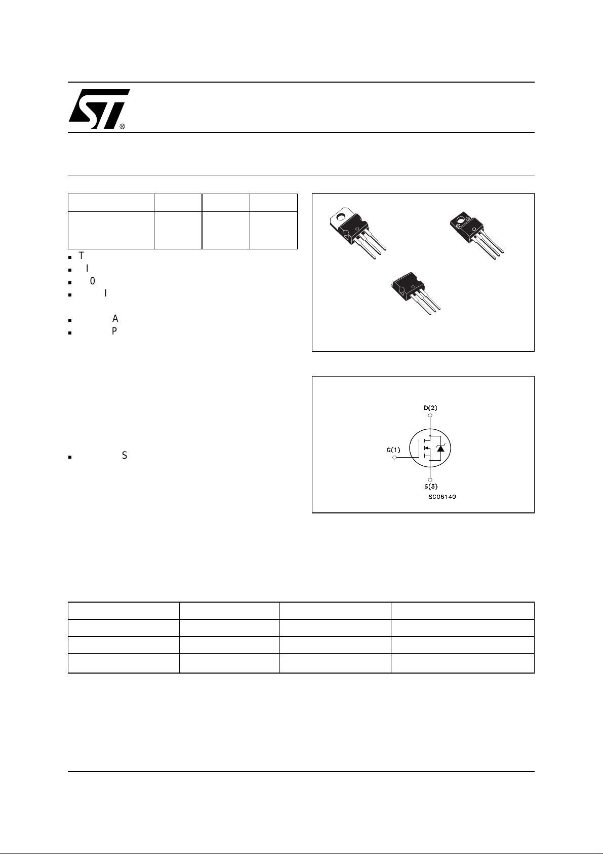
3
2
TO-220
1
TO-220FP
3
2
1
2
PAK
I
1
INTERNAL SCHEM ATIC DIAGRAM
3
2
ORDERING INFORMATION
SALES TYPE MARKING PACKAGE PACKAGING
STP11NM60FD P11NM60FD TO-220 TUBE
STP11NM60FDFP P11NM60FDFP TO-220FP TUBE
STB11NM60FD-1 B11NM60FD-1
I
2
PAK
TUBE
1/11September 2003
STP11NM60FD - STP11NM60FDFP - STB11NM60FD-1
ABSOLUTE MAX IMUM RATINGS
Symbol Parameter Value Unit
V
DS
V
DGR
V
GS
I
D
I
D
I
DM
P
TOT
Drain-source Voltage (VGS=0)
Drain-gate Voltage (RGS=20kΩ)
Gate- source Voltage ±30 V
Drain Current (continuos) at TC= 25°C
Drain Current (continuos) at TC= 100°C
()
Drain Current (pulsed) 44 44 (*) A
Total Dissipation at TC= 25°C
Derating Factor 0.88 0.28 W/°C
1) Peak Diode Recovery voltage slope 20 V/ns
dv/dt (
V
ISO
T
stg
T
j
(•)Pulse width limited by safe operating area
(1)I
<11A, di/dt<400A/µs, VDD<V
SD
(*)Limited only by maximum temperature allowed
Insulation Winthstand Voltage (DC) -- 2500 V
Storage Temperature
Max. Operating Junction Temperature
(BR)DSS,TJ<TJMAX
STP11NM60FD
STB11NM60FD-1
11 11 (*) A
77(*)A
160 35 W
STP11NM60FDFP
600 V
600 V
–65 to 150 °C
THERMAL DATA
2
TO-220/I
PAK TO-220FP
Rthj-case Thermal Resistance Junction-case Max 0.78 3.57 °C/W
Rthj-amb Thermal Resistance Junction-ambient Max 62.5 °C/W
T
l
Maximum Lead Temperature For Soldering Purpose 300 °C
AVALANCHE CHARACTERISTICS
Symbol Parameter Max Value Unit
I
AR
E
AS
Avalanche Current, Repetitive or Not-Repetitive
(pulse width limited by T
max)
j
Single Pulse Avalanche Energy
(starting T
= 25 °C, ID=IAR,VDD=35V)
j
ELECTRICAL CHARACTE RISTICS (T
= 25 °C UNLESS OTHERWISE SPECIFIED)
CASE
5.5 A
350 mJ
ON/OFF
Symbol Parameter Test Conditions Min. Typ. Max. Unit
V
(BR)DSS
I
DSS
I
GSS
V
GS(th)
R
DS(on)
Drain-source
Breakdown Voltage
Zero Gate Voltage
Drain Current (V
GS
=0)
Gate-body Leakage
Current (V
DS
=0)
Gate Threshold Voltage
Static Drain-source On
Resistance
ID= 250 µA, VGS= 0 600 V
V
= Max Rating
DS
= Max Rating, TC= 125 °C
V
DS
V
= ±30V ±100 nA
GS
V
DS=VGS,ID
= 250 µA
34
1µA
100 µA
5V
VGS=10V,ID= 5.5 A 0.40 0.45 Ω
2/11
STP11NM60FD - STP11NM60FDFP - STB11NM60FD-1
DYNAMIC
Symbol Parameter Test Conditions Min. Typ. Max. Unit
(1) Forward Transconductance VDS>I
g
fs
D(on)xRDS(on)max,
ID= 5.5A
V
C
iss
C
oss
C
rss
Input Capacitance
Output Capacitance 208 pF
Reverse Transfer
=25V,f=1MHz,VGS=0
DS
Capacitance
C
oss eq.
(2) Equivalent Output
VGS=0V,VDS= 0V to 400V 100 pF
Capacitance
R
G
Gate Input Resistance f=1 MHz Gate DC Bias = 0
Test Signal Level = 20mV
Open Drain
Note: 1. Pulsed: Pulse duration = 300 µs, duty cycle 1.5 %.
2. C
is defined as a constant equivalent capacitance giving the same charging time as C
oss eq.
V
.
DSS
SWITCHING ON
Symbol Parameter Test Conditions Min. Typ. Max. Unit
V
t
d(on)
Q
Q
Q
Turn-on Delay Time
t
r
g
gs
gd
Rise Time 16 ns
Total Gate Charge
Gate-Source Charge 7.8 nC
Gate-Drain Charge 13 nC
=250V,ID= 5.5A
DD
= 4.7Ω VGS=10V
R
G
(see test circuit, Figure 3)
V
=400V,ID= 11A,
DD
V
=10V
GS
5.2 S
1000 pF
28 pF
3 Ω
when VDSincreases from 0 to 80%
oss
20 ns
28 40 nC
SWITCHING OFF
Symbol Parameter Test Conditions Min. Typ. Max. Unit
V
t
r(Voff)
t
Off-voltage Rise Time
t
f
c
Fall Time 15 ns
Cross-over Time 24 ns
= 400V, ID= 11A,
DD
R
=4.7Ω, VGS= 10V
G
(see test circuit, Figure 5)
10 ns
SOURCE DRAIN DIODE
Symbol Parameter Test Conditions Min. Typ. Max. Unit
I
SD
I
SDM
VSD(1)
t
rr
Q
rr
I
RRM
Note: 1. Pulsed: Pulse duration = 300 µs, duty cycle 1.5 %.
2. Pulse width limited bysafeoperating area.
Source-drain Current 11 A
(2)
Source-drain Current (pulsed) 44 A
Forward On Voltage
Reverse Recovery Time
Reverse Recovery Charge 1.1 µC
ISD= 11A, VGS=0
I
= 11A, di/dt = 100A/µs,
SD
V
=50V
DD
(see test circuit, Figure 5)
190 ns
Reverse Recovery Current 14.5 A
1.5 V
3/11
STP11NM60FD - STP11NM60FDFP - STB11NM60FD-1
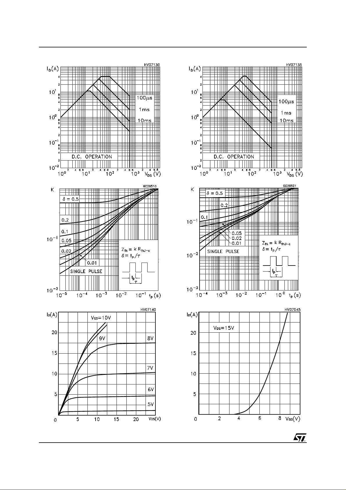
Safe Operating for TO-220/I2PAK Safe Operating Area for TO-220FP
Thermal Impedance for TO-220FPThermal Impedance for TO-220/I2PAK
4/11
Transfer CharacteristicsOutput Characteristics
 Loading...