

SGS Thomson Microelectronics STP11NM60A, STP11NM50AFP, STB11NM60A-1 Datasheet
1/11March 2002
STP11NM60A
STP11NM6 0AFP - STB11NM6 0A- 1
N-CHANNEL 600V - 0.4Ω - 11A TO-220/TO-220FP/I2PAK
MDmesh™Power MOSFET
n
TYPICAL RDS(on) = 0.4Ω
n
HIGH dv/dt
n
LOW INPUT CAPACITANCE AND GATE
CHARGE
n
LOW GATE INPUT RESIST ANC E
DESCRIPTION
The MDmesh™
is a new revolutionary MOSFET
technology that associates the Multiple Drain process with the Company’s PowerMESH™ horizontal
layout. The resulting product has an outstanding low
on-resistance, impressively high dv/dt. The adoption
of the Company’s proprietary strip technique yields
overall dynamic performance that is significantly
better than that of similar competition’s products.
APPLICATIONS
The MDmesh™ family is very suitable for increasing
power density of high voltage converters allowing
system miniaturization and higher efficiencies.
ORDERING INFORMATION
TYPE V
DSS
R
DS(on)
I
D
STP11NM60A
STP11NM60AFP
STB11NM60A-1
600 V
600 V
600 V
<0.45Ω
<0.45Ω
<0.45Ω
11 A
11 A
11 A
SALES TYPE MARKING PACKAGE PACKAGING
STP11NM60A P11NM60A TO-220 TUBE
STP11NM60AFP P11NM60AFP TO-220FP TUBE
STB11NM60A-1 B11NM60A
I
2
PAK
TUBE
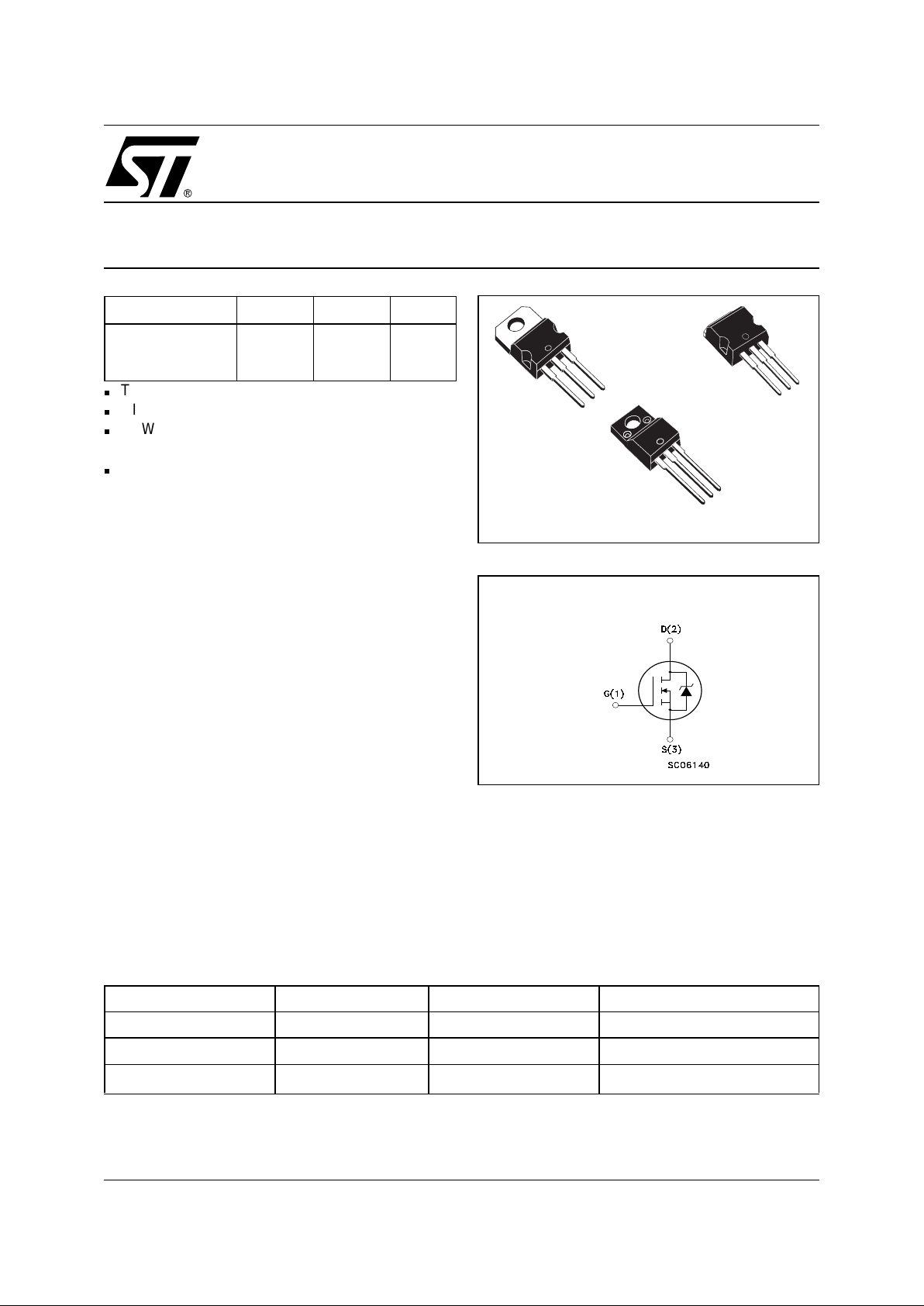
TO-220
1
2
3
1
2
3
I2PAK
1
2
3
TO-220FP
INTERNAL SCHEMATIC DIAGRAM
STP11NM60A/STP11NM60AF P/ST B 11NM60A-1
2/11
ABSOLUTE MAXIMUM RATINGS
(l) Pulse wi dth limited by saf e operating ar ea
(1) I
SD
≤11A, di/dt ≤200A/µs, VDD ≤ V
(BR)DSS
, Tj ≤ T
JMAX.
(*) Limited only by maximum temperature allowed
THERMA L D ATA
ON/OFF
Symbol Parameter Value Unit
STP11NM60A
STB11NM60A-1
STP11NM60AF P
V
DS
Drain-source Voltage (VGS = 0)
600 V
V
DGR
Drain-gate Voltage (RGS = 20 kΩ)
600 V
V
GS
Gate- source Voltage ± 30 V
I
D
Drain Current (continuous) at TC = 25°C
11 11 (*) A
I
D
Drain Current (continuous) at TC = 100°C
7 7 (*) A
I
DM
(l)
Drain Current (pulsed) 44 44 (*) A
P
TOT
Total Dissipation at TC = 25°C
110 35 W
Derating Factor 0.88 0.28 W/°C
dv/dt (1) Peak Diode Recovery voltage slope 15 V/ns
V
ISO
Insulation Withstand Voltage (DC) - 2500 V
T
j
T
stg
Operating Junction Temperature
Storage Temperature
-55 to 150
-55 to 150
°C
°C
TO-220 / I
2
PAK
TO-220-FP
Rthj-case Thermal Resistance Junction-case Max 1.13 3.57 °C/W
Rthj-amb Thermal Resistance Junction-ambient Max 62.5 °C/W
T
l
Maximum Lead Temperature For Soldering Purpose 300
°C
Symbol Parameter Test Conditions Min. Typ. Max. Unit
V
(BR)DSS
Drain-source
Breakdown Voltage
ID = 250 µA, VGS = 0 600 V
I
DSS
Zero Gate Voltage
Drain Current (V
GS
= 0)
V
DS
= Max Rating
VDS = Max Rating, TC = 125 °C
1
10
µA
µA
I
GSS
Gate-body Leakage
Current (V
DS
= 0)
V
GS
= ± 20V ±100 nA
V
GS(th)
Gate Threshold Voltage
V
DS
= VGS, ID = 250µA
234V
R
DS(on)
Static Drain-source On
Resistance
VGS = 10V, ID = 5.5 A 0.4 0.45 Ω
3/11
STP11NM60A/STP11NM60AF P/ST B 11N M 60A-1
ELECTRICAL CHARACTERISTICS (TCASE =25°C UNLESS OTHERWISE SPECIFIED)
DYNAMIC
SWITCHING ON
SWITCHING OFF
SOURCE DRAIN DIODE
Note: 1. Pulsed: Pu l se duration = 300 µs, duty cycle 1. 5 %.
2. Pulse width li mited by safe operating area .
3. C
oss eq.
is defined as a constant equivalent capacitance giving the same charging time as C
oss
when VDS increase s fr om 0 to 80%
V
DSS
.
Symbol Parameter Test Conditions Min. Typ. Max. Unit
g
fs
(1) Forward Transconductance VDS = 15 V, ID= 5.5 A 10 S
C
iss
C
oss
C
rss
Input Capacitance
Output Capacitance
Reverse Transfer
Capacitance
V
DS
= 25V, f = 1 MHz, VGS = 0 1211
248
21
pF
pF
pF
C
oss eq.
(3) Equivalent Output
Capacitance
VGS = 0V, VDS = 0V to 480V 116 pF
R
G
Gate Input Resistance f=1 MHz Gate DC Bias = 0
Test Signal Level = 20mV
Open Drain
1.9 Ω
Symbol Parameter Test Conditions Min. Typ. Max. Unit
t
d(on)
t
r
Turn-on Delay Time
Rise Time
VDD = 300 V, ID = 5.5 A
RG= 4.7Ω VGS = 10 V
(Resistive Load see, Figure 3)
14
15
ns
ns
Q
g
Q
gs
Q
gd
Total Gate Charge
Gate-Source Charge
Gate-Drain Charge
VDD = 480V, ID = 11 A,
VGS = 10V
35
9
14
49
nC
nC
nC
Symbol Parameter Test Conditions Min. Typ. Max. Unit
t
r(Voff)
t
f
t
c
Off-voltage Rise Time
Fall Time
Cross-over Time
V
DD
= 480V, ID = 11 A,
RG=4.7Ω, V
GS
= 10V
(Inductive Load see, Figure 5)
39
10
20
ns
ns
ns
Symbol Parameter Test Conditions Min. Typ. Max. Unit
I
SD
I
SDM
(2)
Source-drain Current
Source-drain Current (pulsed)
11
44
A
A
VSD (1)
Forward On Voltage
ISD = 11 A, VGS = 0
1.5 V
t
rr
Q
rr
I
RRM
Reverse Recovery Time
Reverse Recovery Charge
Reverse Recovery Current
I
SD
= 11 A, di/dt = 100A/µs
VDD = 100V, Tj = 150°C
(see test circuit, Figure 5)
560
5.7
20.5
ns
µC
A
STP11NM60A/STP11NM60AF P/ST B 11NM60A-1
4/11
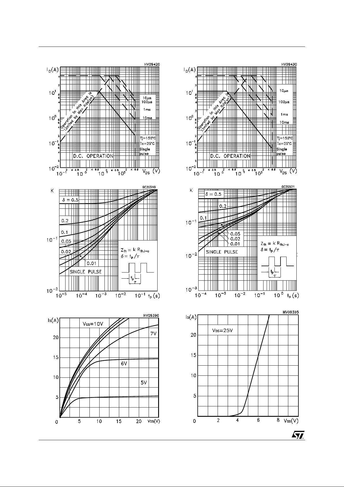
Thermal Impedan ce for TO- 2 20 / I2PAK
Transfer CharacteristicsOutput Characteristics
Safe Operating Area for TO-220FPSafe Operating Area for TO-220 / I2PAK
Thermal Impedance for TO-220FP
 Loading...