

SGS Thomson Microelectronics STP11NM60 Datasheet
STP11NM60
N-CHANNEL 600V - 0.4Ω - 11A TO-220
MDmeshPower MOSFET
PRELIMINARY DATA
TYPE V
STP11NM60 600V <0.45Ω 11 A
■ TYPICAL R
■ HIGH dv/dt AND AVALANCHE CAPABILITIES
■ 100% AVALANCHE TESTED
■ LOW INPUT CAPACITANCE AND GATE
DS
DSS
(on) = 0.4Ω
R
DS(on)
I
D
CHARGE
■ LOW GATEINPUT RESISTANCE
■ TIGHT PROCESS CONTROL AND HIGH
MANUFACTURING YIELDS
DESCRIPTION
The MDmesh is a new revolutionary MOSFET
technology that associates the Multiple Drain process with the Company’s PowerMESH horizontal
layout. The resulting producthas an outstanding low
on-resistance, impressively high dv/dt and excellent
avalanche characteristics. The adoption of the
Company’s proprietary strip technique yields overall
dynamic performancethat is significantly better than
that of similar competition’s products.
APPLICATIONS
The MDmesh familyisverysuitable for increasing
power density of high voltage converters allowing
system miniaturization and higher efficiencies.
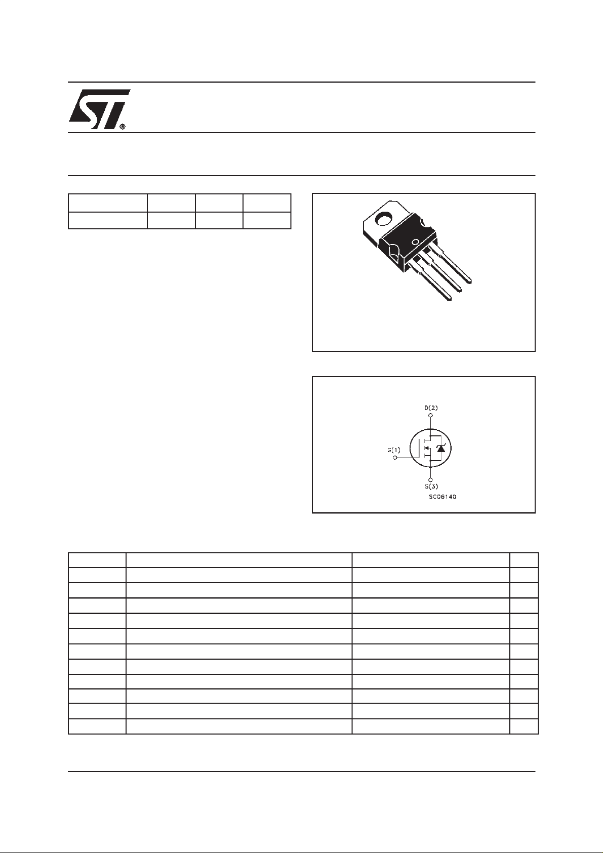
3
2
1
TO-220
INTERNAL SCHEMATIC DIAGRAM
ABSOLUTE MAXIMUM RATINGS
Symbol Parameter Value Unit
V
DS
V
DGR
V
GS
I
D
I
D
I
DM
P
TOT
dv/dt(1) Peak Diode Recovery voltage slope 6 V/ns
T
stg
T
j
(•)Pulse width limitedby safe operating area
(1)I
<11A, di/dt<200A/µs, VDD<V
SD
May 2000
Drain-source Voltage (VGS= 0) 600 V
Drain-gate Voltage (RGS=20kΩ) 600 V
Gate- source Voltage ±30 V
Drain Current (continuos) at TC=25°C11A
Drain Current (continuos) at TC= 100°C7A
(●) Drain Current (pulsed) 44 A
TotalDissipation at TC=25°C
Derating Factor 0.88 W/°C
Storage Temperature –65 to 150 °C
Max. Operating Junction Temperature 150 °C
(BR)DSS,TJ<TJMAX
110 W
1/6
STP11NM60
THERMAL DATA
Rthj-case Thermal Resistance Junction-case Max 1.13 °C/W
Rthj-amb Thermal Resistance Junction-ambient Max 62.5 °C/W
Rthc-sink Thermal Resistance Case-sink Typ 0.5 °C/W
T
l
AVALANCHE CHARACTERISTICS
Symbol Parameter Max Value Unit
I
AR
E
AS
ELECTRICAL CHARACTERISTICS (TCASE = 25 °C UNLESS OTHERWISE SPECIFIED)
OFF
Symbol Parameter Test Conditions Min. Typ. Max. Unit
V
(BR)DSS
I
DSS
I
GSS
Maximum Lead Temperature For Soldering Purpose 300 °C
Avalanche Current, Repetitive or Not-Repetitive
(pulse width limited by T
max)
j
Single Pulse Avalanche Energy
(starting T
Drain-source
Breakdown Voltage
Zero Gate Voltage
Drain Current (V
Gate-body Leakage
Current (V
=25°C, ID=IAR,VDD=50V)
j
I
= 250 µA, VGS=0
D
= Max Rating
V
DS
=0)
DS
GS
=0)
V
= Max Rating, TC= 125 °C
DS
= ±30V
V
GS
600 V
11 A
400 mJ
1 µA
10 µA
±100 nA
ON (1)
Symbol Parameter Test Conditions Min. Typ. Max. Unit
V
GS(th)
R
DS(on)
I
D(on)
Gate Threshold Voltage
Static Drain-source On
Resistance
On State Drain Current
V
DS=VGS,ID
= 10V, ID= 5.5A
V
GS
V
DS>ID(on)xRDS(on)max,
= 250µA
VGS=10V
345V
0.4 0.45 Ω
11 A
DYNAMIC
Symbol Parameter Test Conditions Min. Typ. Max. Unit
V
g
(1)
fs
C
iss
C
oss
C
rss
R
G
Note: 1. Pulsed: Pulse duration = 300 µs, duty cycle 1.5%.
Forward Transconductance
Input Capacitance
Output Capacitance 220 pF
Reverse Transfer
Capacitance
Gate Input Resistance
DS>ID(on)xRDS(on)max,
ID= 5.5A
V
= 25V, f = 1 MHz, VGS=0
DS
f=1 MHz Gate DC Bias = 0
Test Signal Level = 20mV
Open Drain
5.2 S
980 pF
20 pF
1.6 Ω
2/6
 Loading...