

SGS Thomson Microelectronics STN851 Datasheet

®
LOW VOLTAGE FAST-SWITCHING
Ordering Code Marking Shipment
STN851 N851 Tape & Reel
■ VERY LOW CO LLECT O R TO EMITTER
SATURATION VOLTAGE
■ HIGH CURRENT GAIN CHARACTE RIS TIC
■ FAST-SWITCHIN G SPE ED
■ SURFACE-MOUNTING SOT-223 MEDIUM
POWER PACKAGE IN TAPE & REEL
APPLICATIONS:
■ EMERGENCY LIGHTING
■ VOLTAG E REG UL A TO RS
■ RELAY DRIVERS
■ HIGH EFFICIE NCY LO W VO LT AGE
SWITCHING APPLICATIONS
DESCRIPTION
The device is manufactured in NPN Planar
Technology by using a "Base Island" layout.
The resulting Transistor shows exceptional high
gain performance coupled with very low
saturation voltage.
STN851
NPN POWER TRANSISTOR
PRELIMINARY DATA
2
3
2
1
SOT-223
INTERNAL SCHEMATIC DIAGRAM
ABSOL UT E MAXIMU M RATINGS
Symbol Parameter Value Unit
V
V
V
I
I
P
T
September 2003
Collector-Base Voltage (IE = 0) 150 V
CBO
Collector-Emitter Voltage (IB = 0) 60 V
CEO
Emitter-Base Voltage (IC = 0) 7 V
EBO
I
Collector Current 5 A
C
Collector Peak Current (tp < 5 ms) 10 A
CM
I
Base Current 1 A
B
Base Peak Current (tp < 5 ms) 2 A
BM
Total Dissipation at T
tot
Storage Temperature -65 to 150
stg
T
Max. Operating Junction Temperature 150
j
= 25 oC 1.6 W
amb
o
C
o
C
1/7
STN851
THERMAL DATA
R
thj-amb
• Device mo unte d on a P.C.B . ar ea of 1 cm
Thermal Resistance Junction-ambient Max 78
o
2
C/W
ELECTRICAL CHARACTERISTICS (T
= 25 oC unless otherwise specified)
case
Symbol Parameter Test Conditions Min. Typ. Max. Unit
I
CBO
I
EBO
V
(BR)CBO
Collector Cut-off
Current (I
= 0)
E
Emitter Cut-off Current
(I
= 0)
C
Collector-Base
= 120 V
V
CB
V
= 120 V Tj = 100 oC
CB
= 7 V 10 nA
V
EB
= 100 µA
I
C
150 V
50
1
Breakdown Voltage
(I
= 0)
E
V
(BR)CEO
∗ Collector-Emitter
I
= 10 mA 60 V
C
Breakdown Voltage
(I
= 0)
B
V
(BR)EBO
Emitter-Base
= 100 µA
I
E
7V
Breakdown Voltage
(I
= 0)
C
V
∗ Collector-Emitter
CE(sat)
Saturation Voltage
V
∗ Base-Emitter
BE(sat)
IC = 100 mA IB = 5 mA
I
= 1 A IB = 50 mA
C
I
= 2 A IB = 50 mA
C
I
= 5 A IB = 200 mA
C
10
70
140
320
IC = 4 A IB = 200 mA 1 1.15 V
50
120
250
500
Saturation Voltage
∗ Base-Emitter On
V
BE(on)
IC = 4 A VCE = 1 V 0.89 1 V
Voltage
∗ DC Current Gain IC = 10 mA VCE = 1 V
h
FE
f
C
CBO
Transition frequency V
T
Collector-Base
I
= 2 A VCE = 1 V
C
I
= 5 A VCE = 1 V
C
I
= 10 A VCE = 1 V
C
= 10 V IC = 100 mA 130 MHz
CE
VCB = 10 V f = 1 MHz 50 pF
150
150
90
30
300
270
140
50
350
Capacitance
RESISTIVE LOAD
on
s
t
f
Turn- on Time
Storage Time
Fall Time
t
t
* Pulsed: Pulse duration = 300µs, duty cycle = 1.5 %
I
= 1 A VCC = 10 V
C
I
= - IB2 = 0.1 A
B1
50
1.35
120
nA
µA
mV
mV
mV
mV
ns
µs
ns
2/7
STN851
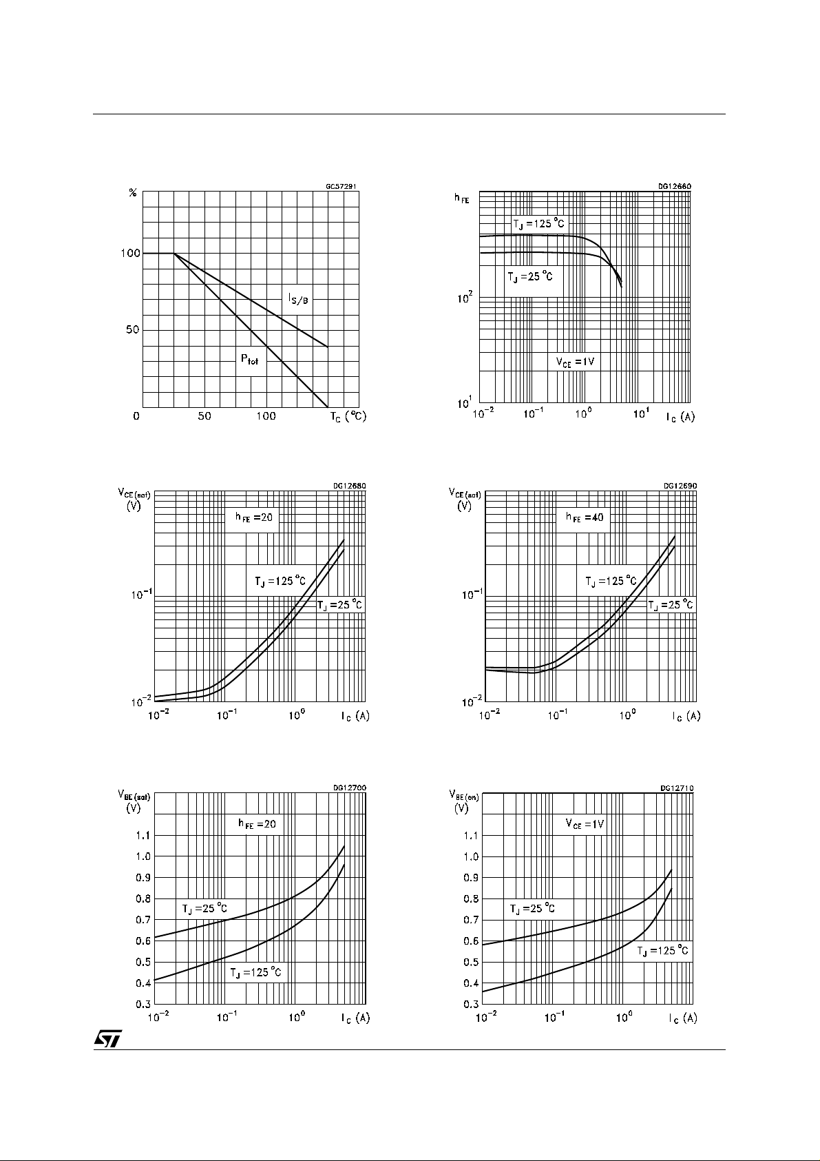
Derating Curve
DC Current Gain
Collector-Em itter Sat uration Volt ag e Collector-Emitter Saturation Voltage
Base-Emitter Saturation Voltage Base-Emitter On Voltage
3/7
 Loading...