


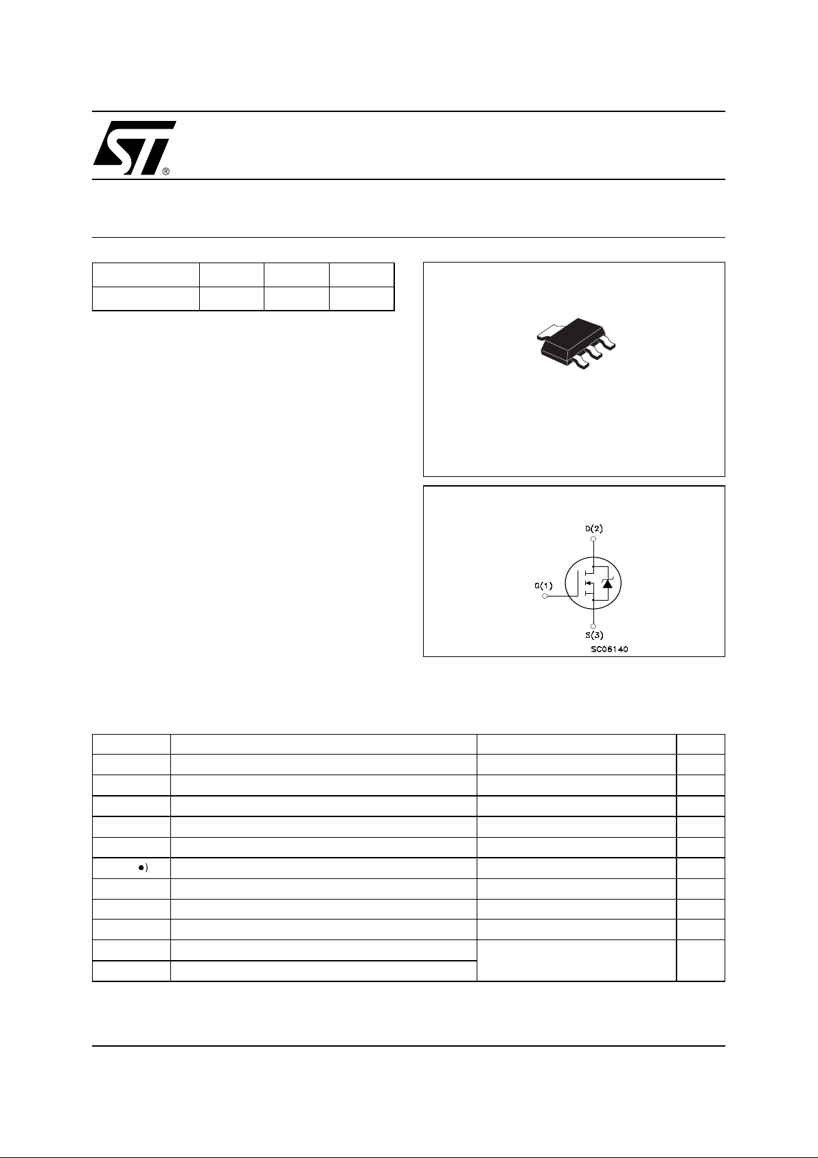
STN4NF03L
N-CHANNEL 30V - 0.039Ω -6.5ASOT-223
STripFET™ II POWER M OSFET
TYPE V
DSS
R
DS(on)
I
D
STN4NF03L 30V <0.05Ω 6.5A
■ TYPICAL R
■ LOW T HRE S HOLD DRIVE
(on) = 0.039Ω
DS
DESCRIPTION
This Power Mosfet is the latest development of STMicroelectronics unique “Single Feature Size™
” strip-
based process. The resulting transistor shows extremely high packing d ens ity for low on-resistance,
rugged avalance characteristics and less critical alignment steps therefore a remarkable manufacturing reproducibility.
APPLICATIONS
■ DC-DC & DC-AC CONVERTERS
■ DC MOTO R CONTROL (DISK DRIVES, etc.)
■ SYNCHRONOUS RECTIFICATION
2
3
2
1
SOT-223
INTERNAL SCHE M ATIC DIAGRAM
ABSOLUTE MAX IMUM RATINGS
Symbol Parameter Value Unit
V
DS
V
DGR
V
GS
I
D
I
D
I
DM
P
TOT
E
AS
T
stg
T
j
(●) Pulse width limited by safe operating area
Drain-source Voltage (VGS=0)
Drain-gate Voltage (RGS=20kΩ)
30 V
30 V
Gate- source Voltage ±16 V
Drain Current (continuous) at TC= 25°C
Drain Current (continuous) at TC= 100°C
()
Drain Current (pulsed) 26 A
Total Dissipation at TC= 25°C
6.5 A
4.5 A
3.3 W
Derating Factor 0.026 W/°C
(1)
Single Pulse Avalanche Energy 200 mJ
Storage Temperature
Operating Junction Temperature
(1) Starting Tj=25°C, ID=6.5A, VDD=15V
–55 to 175 °C
1/8December 2002
STN4NF03L
THERMAL DATA
Rthj-PCB Thermal Resistance Junction-PC Board Max (*) 38 °C/W
Rthj-PCB Thermal Resistance Junction-PCB Max (**) 100 °C/W
T
l
Note: (*) When mounted on 1 in2FR-4 board , 2 oz Cu, t<10s.
Note: (**) Minimum recommended footprint
Maximum Lead Temperature For Soldering Purpose
(1.6 mm from case for 10s)
260 °C
ELECTRICAL CHARACTE RISTICS (T
= 25 °C UNLESS OTHERWISE SPECIFIED)
CASE
OFF
Symbol Parameter Test Conditions Min. Typ. Max. Unit
V
(BR)DSS
Drain-source
ID= 250 µA, VGS= 0 30 V
Breakdown Voltage
I
DSS
I
GSS
Zero Gate Voltage
Drain Current (V
GS
Gate-body Leakage
Current (V
DS
=0)
=0)
V
= Max Rating
DS
= Max Rating, TC= 125 °C
V
DS
V
= ±16V ±100 nA
GS
10 µA
1µA
ON (1)
Symbol Parameter Test Conditions Min. Typ. Max. Unit
V
GS(th)
R
DS(on)
Gate Threshold Voltage
Static Drain-source On
Resistance
V
DS=VGS,ID
=10V,ID=2A
V
GS
=5V,ID=2A
V
GS
= 250 µA
1V
0.039 0.05 Ω
0.046 0.06 Ω
DYNAMIC
Symbol Parameter Test Conditions Min. Typ. Max. Unit
(1)
g
fs
C
iss
C
oss
C
rss
Forward Transconductance
Input Capacitance
Output Capacitance 90 pF
Reverse Transfer
Capacitance
VDS=10V,ID=2 A
V
=25V,f=1MHz,VGS=0
DS
13 S
330 pF
40 pF
2/8

STN4NF03L
ELECTRICAL CHARACTE RISTICS (CONTINUED)
SWITCHING ON
Symbol Parameter Test Conditions Min. Typ. Max. Unit
t
d(on)
Q
Q
Q
t
r
g
gs
gd
Turn-on Delay Time VDD=15V,ID=2A
= 4.7Ω VGS=4.5V
R
Rise Time 100 ns
Total Gate Charge
Gate-Source Charge
Gate-Drain Charge
G
(see test circuit, Figure 3)
VDD=24V,ID=4A,
V
=10V
GS
SWITCHING OFF
Symbol Parameter Test Conditions Min. Typ. Max. Unit
t
d(off)
Turn-off-Delay Time VDD=15V,ID=2A,
RG=4.7Ω, VGS= 4.5 V
(see test circuit, Figure 3)
t
f
Fall Time 22 ns
SOURCE DRAIN DIODE
Symbol Parameter Test Conditions Min. Typ. Max. Unit
I
SD
I
SDM
V
SD
t
rr
Q
rr
I
RRM
Note: 1. Pulsed: Pulse duration = 300 µs, duty cycle 1.5 %.
2. Pulse width limited by safe operating area.
Source-drain Current
(2)
Source-drain Current (pulsed)
(1)
Forward On Voltage
Reverse Recovery Time
Reverse Recovery Charge
Reverse Recovery Current
ISD= 6.5 A, VGS=0
= 6.5 A, di/dt = 100 A/µs,
I
SD
VDD=15V,Tj= 150°C
(see test circuit, Figure 5)
11 ns
6.5
9nC
3.6
2
25 ns
6.5
26
1.5 V
35
25
1.4
nC
nC
A
A
ns
nC
A
Safe Operating Area
Thermal Impedence Junction-PCB
3/8