

SGS Thomson Microelectronics STN4NE03 Datasheet
STN4NE03
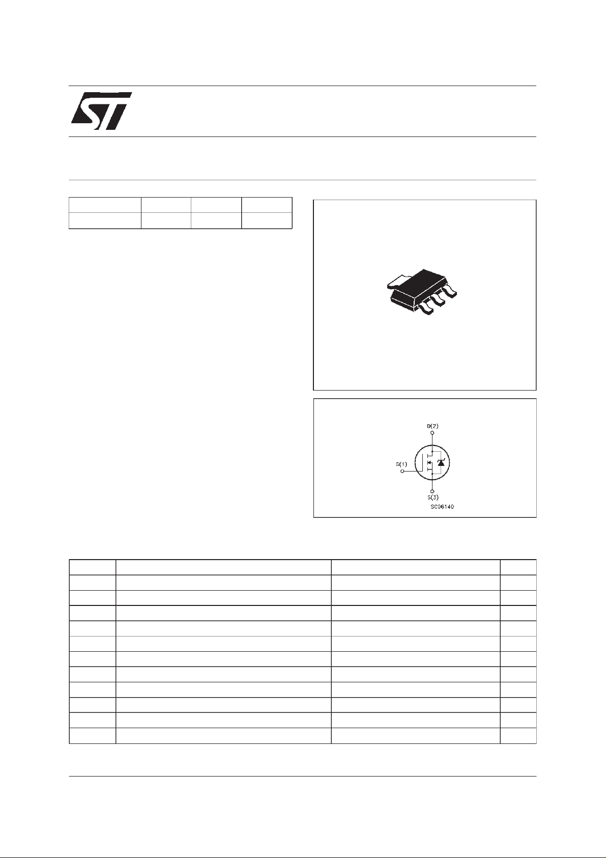
N - CHANNEL 30V - 0.045Ω - 4A - SOT-223
STripFET POWER MOSFET
TYPE V
DSS
R
DS(on)
I
D
STN4N E03 30 V < 0.06 Ω 4A
■ TYPICALR
■ EXCEPTIONALdv/dt CAPABILITY
■ AVALANCHERUGGEDTECHNOLOGY
■ 100% AVALANCHETESTED
■ APPLICATIONORIENTED
DS(on)
=0.045 Ω
CHARACTERIZATION
DESCRIPTION
This Power MOSFET is the latestdevelopmentof
STMicroelectronics unique ” Single Feature
”
Size
strip-based process. The resulting
transistor shows extremely high packing density
for low on-resistance, rugged avalanche
characteristics and less critical alignment steps
therefore a remarkable manufacturing
reproducibility.
APPLICATIONS
■ DC MOTOR CONTROL (DISK DRIVES, etc.)
■ DC-DC& DC-AC CONVERTERS
■ SYNCHRONOUSRECTIFICATION
■ POWERMANAGEMENT IN
BATTERY-OPERATEDAND PORTABLE
EQUIPMENT
2
3
2
1
SOT-223
INTERNAL SCHEMATIC DIAGRAM
ABSOLUTE MAXIMUM RATINGS
Symbol Parameter Value Unit
V
V
DGR
V
I
D
I
D
I
DM
P
dv/dt (
T
(•) Pulse width limited by safe operating area (*) Limited by package (1)ISD≤ 10A, di/dt ≤ 300A/µs, VDD≤ V
August 1998
Drain-s ou r ce Voltage (VGS=0) 30 V
DS
Drain- gat e Volt ag e (RGS=20kΩ)
Gate-source Vol tage ± 20 V
GS
30 V
(*) Drain Cur r en t (continu ous) at Tc=25oC4A
(*) Drain Cur r en t (continu ous) at Tc=100oC2.5A
(•) Dr ain Curren t ( p ulsed) 16 A
Tot al Di s sipa t ion at Tc=25oC2.5W
tot
Derat ing Factor 0.02 W/
1) Peak Diode Recovery volta ge slope 6 V/ns
Storage Temperature -65 to 150
stg
T
Max. Oper ating Jun ct io n T e m pe r ature 150
j
(BR)DSS
,Tj≤T
o
C
o
C
o
C
jMAX
1/8
STN4NE03
THERMAL DATA
R
thj-pcb
R
thj- amb
T
AVALANCHE CHARACTERISTICS
Symbol Para met e r Max Valu e Uni t
I
AR
E
Ther mal Resist ance Junctio n- PC Board Max
Ther mal Resist ance Junctio n- ambient Max
(Sur f a ce M ounted)
Maximum Lead Tempera t ure For Soldering P urpose
l
Avalanch e C urr e nt , Repetit i v e o r Not-Re petitiv e
(pulse w idth limited by T
Single Pulse Avalanche Energy
AS
(starting T
=25oC, ID=IAR,VDD=25V)
j
max, δ <1%)
j
50
60
260
4A
20 mJ
o
C/W
o
C/W
o
C
ELECTRICAL CHARACTERISTICS (T
=25oC unlessotherwisespecified)
case
OFF
Symbol Parameter Test Condition s Min. Typ. Max. Unit
V
(BR)DSS
Drain-sou rc e
=250µAVGS=0
I
D
30 V
Breakdown Voltage
I
I
DSS
GSS
Zer o Gat e Voltage
Drain Current (V
GS
Gat e-body Le aka ge
Current (V
DS
=0)
=0)
=MaxRating
V
DS
V
=MaxRating Tc=125
DS
o
C
= ± 20 V
V
GS
1
10
± 100 nA
ON (∗)
Symbol Parameter Test Condition s Min. Typ. Max. Unit
V
GS(th )
Gate Threshold
V
DS=VGSID
=250µA
234V
Voltage
R
DS(on)
Stati c Drain-so urce On
VGS=10V ID= 2 A 0.045 0. 0 6 Ω
Resistance
I
D(on)
On Stat e Drain Current VDS>I
D(on)xRDS(on)max
4A
VGS=10V
DYNAMIC
Symbol Parameter Test Condition s Min. Typ. Max. Unit
g
(∗)Forward
fs
Tr anscond uctanc e
C
C
C
Input Ca paci t ance
iss
Out put C apa c itanc e
oss
Reverse Trans fer
rss
Capa cit an c e
VDS>I
D(on)xRDS(on)maxID
=2A 1 3.0 S
VDS=25V f=1MHz VGS= 0 V 760
150
50
1000
200
80
µA
µA
pF
pF
pF
2/8
STN4NE03
ELECTRICAL CHARACTERISTICS (continued)
SWITCHINGON
Symbol Parameter Test Condition s Min. Typ. Max. Unit
t
d(on)
t
r
Turn-on Time
Rise Time
VDD=5V ID=5A
=4.7 Ω VGS=10V
R
G
10
60
(see test circuit, figure 3)
Q
Q
Q
Total Gate Charge
g
Gat e-Sou r ce Cha rge
gs
Gate-Drain Charge
gd
VDD=24V ID=10A VGS=10V 22
7
7
SWITCHINGOFF
Symbol Parameter Test Condition s Min. Typ. Max. Unit
t
r(Voff)
t
t
Of f - voltag e Rise Time
Fall Time
f
Cross-over Time
c
VDD=24V ID=10A
=4.7 Ω VGS=10V
R
G
(see test circuit, figure 5)
8
15
25
SOURCE DRAIN DIODE
Symbol Parameter Test Condition s Min. Typ. Max. Unit
I
SD
I
SDM
V
SD
t
Q
I
RRM
(∗) Pulsed: Pulse duration =300 µs, duty cycle1.5 %
(•) Pulse widthlimited by safe operating area
Source-drain Curre nt
(•)
Source-drain Curre nt
(pulsed)
(∗) Fo rward On Vo lt age ISD=4A VGS=0 1.5 V
Reverse Rec overy
rr
Time
Reverse Rec overy
rr
= 10 A di/dt = 100 A/µs
I
SD
=24V Tj=150oC
V
DD
(see test circuit, figure 5)
40
0.06
Charge
Reverse Rec overy
3.0
Current
15
90
30 nC
15
25
40
4
16
ns
ns
nC
nC
ns
ns
ns
A
A
ns
µC
A
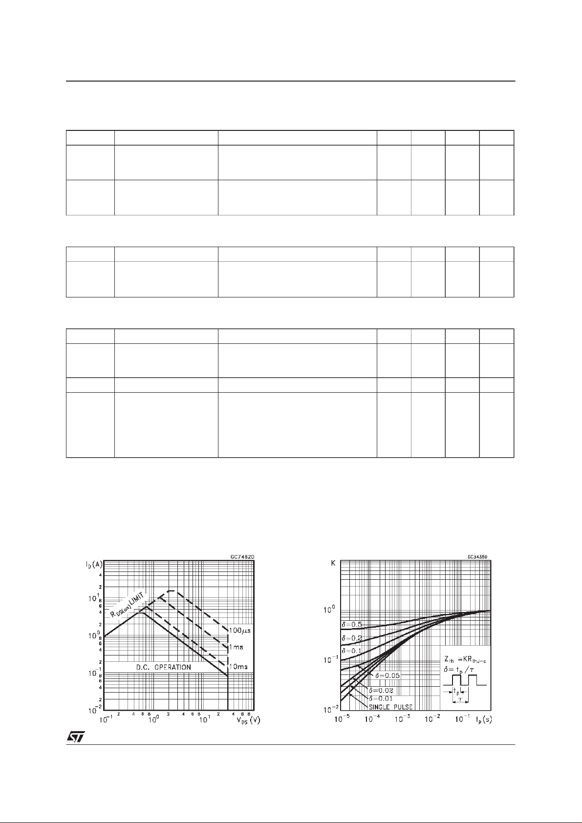
Safe Operating Area ThermalImpedance
3/8
 Loading...