

SGS Thomson Microelectronics STN3NE06L Datasheet
®
N - CHANNEL 60V - 0.10 Ω - 3A - SOT-223
TYPE V
DSS
STN3NE06L 60 V < 0.120 Ω 3 A
R
DS(on)
I
D
STN3NE06L
STripFET POWER MOSFET
PRELIMINARY DATA
■ TYPICAL R
■ EXCEPTI ON AL dv/dt CAP AB ILI TY
■ AVALANCHE RUGGED TECHNOLOGY
■ 100 % AVALANCHE TESTED
■ APPLICATION ORIENT ED
DS(on)
= 0.10 Ω
CHARACTERIZATION
DESCRIPTION
This Power Mosfet is the latest development of
STMicroelectronics unique "Single Feature
Size" stip-based process. The resulting transistor shows extremely high packing density for low
on-resistance, rugged avalanche characteristics
and less critical alignment steps therefore a remarkable manufacturing reproducibility .
APPLICATIONS
■ DC MOTOR CONTROL (DISK DRIVES,etc.)
■ DC-DC & DC-AC CONVERT E RS
■ SYNCHRONOUS RECTIFICATION
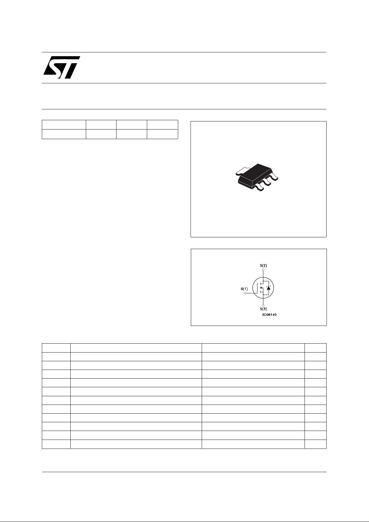
2
3
2
1
SOT-223
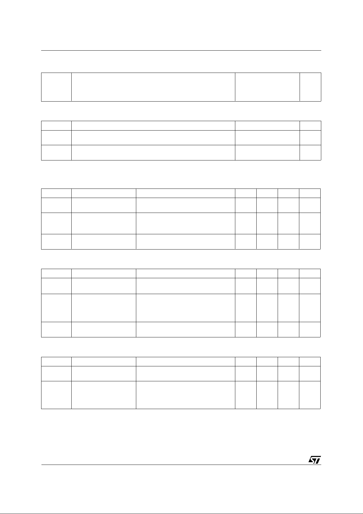
INTER NAL SCH E M ATI C DIAG RA M
ABSOLUTE MAXIMUM RATINGS
Symbol Parameter Value Unit
V
V
V
I
DM
P
dv/dt(
T
(•) Pulse width limited by safe operating area (1) ISD ≤ 12 A, di/dt ≤ 200 A/µs, VDD ≤ V
New RDS (on) spec. starting from JULY 98
August 1998
Drain-source Voltage (VGS = 0) 60 V
DS
Drain- gate Voltage (RGS = 20 kΩ)
DGR
Gate-source Voltage ± 20 V
GS
Drain Current (continuous) at Tc = 25 oC3A
I
D
Drain Current (continuous) at Tc = 100 oC1.8A
I
D
60 V
(•) Drain Current (pulsed) 12 A
Total Dissipation at Tc = 25 oC2.5W
tot
Derating Factor 0.02 W/
1) Peak Diode Recovery voltage slope 6 V/ns
Storage Temperature -65 to 150
stg
T
Max. Operating Junction Temperature 150
j
, Tj ≤ T
(BR)DSS
JMAX
o
C
o
C
o
C
1/5
STN3NE06L
THERMAL DATA
R
thj-pcb
R
thj-amb
Thermal Resistance Junction-PC Board Max
Thermal Resistance Junction-ambient Max
(Surface Mounted)
T
Maximum Lead Temperature For Soldering Purpose
l
AVALANCHE CHARACTERI S TICS
Symbol Parameter Max Value Unit
I
AR
E
Avalanche Current, Repetitive or Not-Repetitive
(pulse width limited by T
Single Pulse Avalanche Energy
AS
(starting T
= 25 oC, ID = IAR, V
j
ma x)
j
DD
= 25 V)
50
60
260
3A
20 mJ
o
C/W
o
C/W
o
C
ELECTRICAL CHARACTERISTICS (T
= 25 oC unless otherwise specified)
case
OFF
Symbol Parameter Test Conditions Min. Typ. Max. Unit
V
(BR)DSS
Drain-source
I
= 250 µA V
D
GS
= 0
60 V
Breakdown Voltage
I
DSS
I
GSS
Zero Gate Voltage
Drain Current (V
GS
Gate-body Leakage
Current (V
DS
= 0)
= 0)
= Max Rating
V
DS
V
= Max Rating Tc = 125
DS
o
C
V
= ± 20 V
GS
1
10
± 100 nA
ON (∗)
Symbol Parameter Test Conditions Min. Typ. Max. Unit
V
GS(th)
Gate Threshold
V
= VGS ID = 250 µA
DS
1 1.7 2.5 V
Voltage
R
DS(on)
I
D(on)
Static Drain-source On
Resistance
VGS = 10 V ID = 6A
V
= 5 V ID = 6A
GS
On State Drain Current VDS > I
V
= 10 V
GS
D(on)
x R
DS(on)max
0.080
3A
0.1
0.100
0.12
DYNAMIC
µA
µA
Ω
Ω
Symbol Parameter Test Conditions Min. Typ. Max. Unit
g
(∗) Forward
fs
VDS > I
D(on)
x R
DS(on)max
ID = 1.5 A 1 3 S
Transconductance
C
C
C
Input Capacitance
iss
Output Capacitance
oss
Reverse Transfer
rss
V
= 25 V f = 1 MHz V
DS
= 0 V 700
GS
100
30
960
140
45
Capacitance
2/5
pF
pF
pF
 Loading...