

SGS Thomson Microelectronics STN2NF06L Datasheet
STN2NF06L
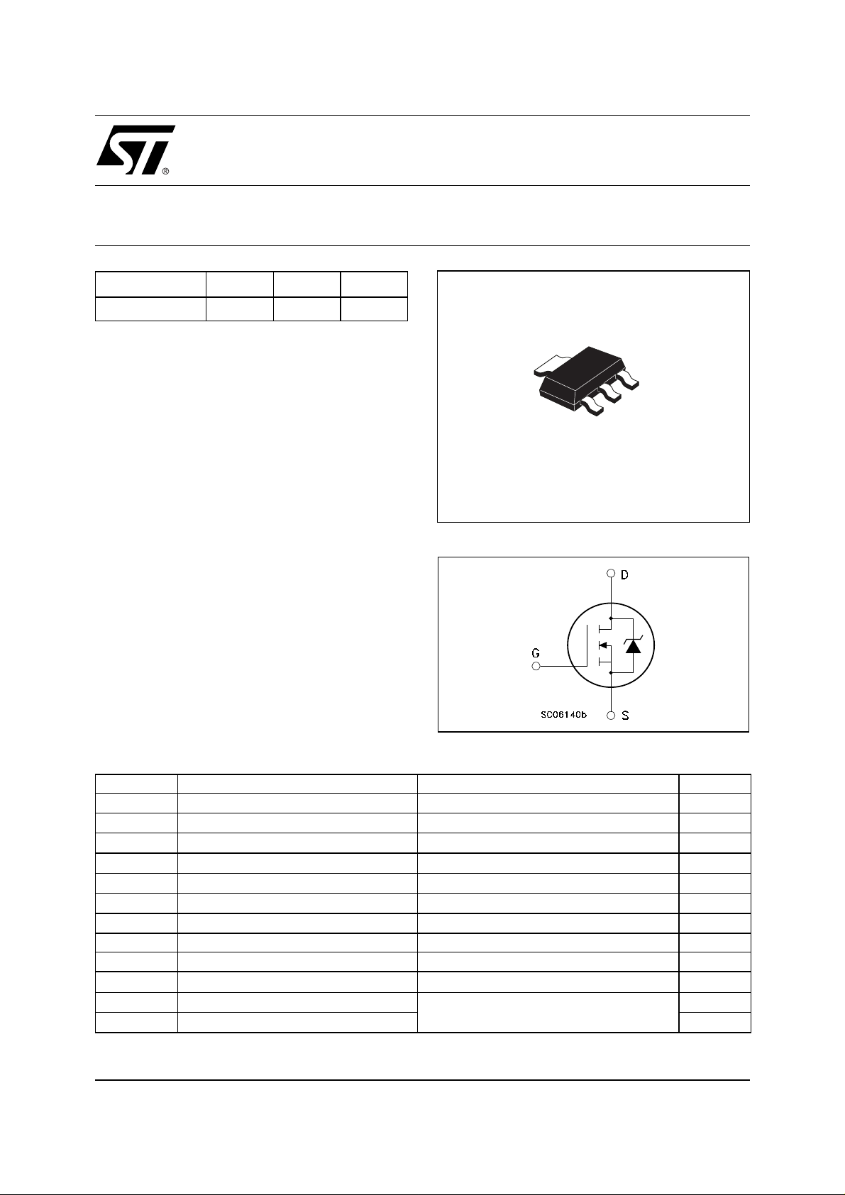
N-CHANNEL 60V - 0.1 Ω - 2A SOT-223
STripFET™ II POWER MOSFET
TYPE
V
DSS
STN2NF06L 60 V <0.12
■ TYPICAL R
■ EXTREMELY HIGH dv /d t C APABILITY
■ 100% AVALANCHE TESTED
■ AVALANCHE RUGGED TECHNOLOGY
■ LOW THRESHOLD DRIVE
(on) = 0.1 Ω
DS
R
DS(on)
I
D
Ω
2 A
DESCRIPTION
This Power MOSFET is the latest dev elo pment of
STMicroelectronis unique "Single Feature Size™"
strip-based process. The resulting transistor
shows extremely high packing density for low onresistance, rugged avalanche characteristics and
less critical alignment steps therefore a remarkable manufacturing reproducibility.
APPLICATIONS
■ DC MOTOR CONTROL (DISK DRIVES, etc.)
■ DC-DC & DC-AC CONVERTERS
■ SYNCHRONOUS RECTIFICATION
2
3
2
1
SOT-223
INTERNAL SCHEMATIC DIAGRAM
ABSOLUTE MAXIMUM RATINGS
Symbol Parameter Value Unit
V
DS
V
DGR
V
GS
I
D
I
D
(
I
DM
(1) Total Dissipation at T
P
tot
dv/dt
E
AS
T
stg
T
j
(
Pulse widt h l i m i ted by safe operating area.
•)
(1)
Related to Rthj -l
.
Drain-source Voltage (VGS = 0)
Drain-gate Voltage (RGS = 20 kΩ)
60 V
60 V
Gate- source Voltage ± 16 V
Drain Current (continuous) at TC = 25°C
Drain Current (continuous) at TC = 100°C
•)
Drain Current (pulsed) 8 A
= 25°C
C
2A
1.2 A
3W
Derating Factor 8 W/°C
(2)
Peak Diode Recovery voltage slope 6 V/ns
(3)
Single Pulse Avalanche Energy 200 mJ
Storage Temperature
Max. Operating Junction Temperature °C
(2) ISD ≤2A, di/dt ≤100A/ µ s , VDD ≤ V
(3) Starting Tj = 25 oC, ID = 2A, VDD = 30V
-55 to 150
(BR)DSS
, Tj ≤ T
°C
JMAX
1/8November 2002
STN2NF06L
THERMA L D ATA
Rthj-pcb
Rthj-pcb
T
l
Thermal Resistance Junction-PCB(1 inch2 copper board)
Thermal Resistance Junction-PCB (min. footprint)
Maximum Lead Temperature For Soldering Purpose
50
90
260
°C/W
°C/W
°C
ELECTRICAL CHARACTERISTICS (T
= 25 °C unless otherwise specified)
case
OFF
Symbol Parameter Test Conditions Min. Typ. Max. Unit
= 250 µA, VGS = 0
V
(BR)DSS
Drain-source
I
D
60 V
Breakdown Voltage
= Max Rating
V
DS
= Max Rating TC = 125°C
V
DS
= ± 16 V
V
GS
1
10
±100 nA
ON
(*)
I
DSS
I
GSS
Zero Gate Voltage
Drain Current (V
GS
Gate-body Leakage
Current (V
DS
= 0)
= 0)
Symbol Parameter Test Conditions Min. Typ. Max. Unit
V
V
GS(th)
R
DS(on)
Gate Threshold Voltage
Static Drain-source On
Resistance
= V
DS
GS
= 10 V ID = 1 A
V
GS
= 5 V ID = 1 A
V
GS
ID = 250 µA
1V
0.1
0.12
0.12
0.14
DYNAMIC
Symbol Parameter Test Conditions Min. Typ. Max. Unit
(*)
g
fs
C
iss
C
oss
C
rss
Forward Transconductance
Input Capacitance
Output Capacitance
Reverse Transfer
Capacitance
V
= 15 V ID = 1 A
DS
= 25V f = 1 MHz VGS = 0
V
DS
3S
360
55
25
µA
µA
Ω
Ω
pF
pF
pF
2/8
STN2NF06L
ELECTRICAL CHARACTERISTICS (continued)
SWITCHING ON
Symbol Parameter Test Conditions Min. Typ. Max. Unit
= 30 V ID = 1 A
t
d(on)
Q
Q
Q
t
r
g
gs
gd
Turn-on Time
Rise Time
Total Gate Charge
Gate-Source Charge
Gate-Drain Charge
SWITCHING OFF
Symbol Parameter Test Conditions Min. Typ. Max. Unit
t
d(off)
t
f
Turn-off Delay Time
Fall Time
SOURCE DRAIN DIODE
Symbol Parameter Test Conditions Min. Typ. Max. Unit
I
SD
I
SDM
V
SD
t
rr
Q
rr
I
RRM
(*)
Pulsed: P ul se duration = 300 µs, duty cycle 1.5 %.
(
•)Pulse width limited by s afe operating area.
Source-drain Current
(•)
Source-drain Current (pulsed)
(*)
Forward On Voltage
Reverse Recovery Time
Reverse Recovery Charge
Reverse Recovery Current
V
DD
= 4.7
R
Ω
G
VGS = 4.5 V
(Resistive Load, Figure 3)
= 48 V ID= 2 A VGS= 5 V
V
DD
= 30 V ID = 1 A
V
DD
= 4.7Ω, V
R
G
GS
= 4.5 V
(Resistive Load, Figure 3)
I
= 2 A VGS = 0
SD
I
= 2 A di/dt = 100A/µs
SD
= 20 V Tj = 150°C
V
DD
(see test circuit, Figure 5)
10
20
5.6
1.2
2.6
17
6
28
31
2.2
7.6 nC
2
8
1.3 V
ns
ns
nC
nC
ns
ns
A
A
ns
nC
A
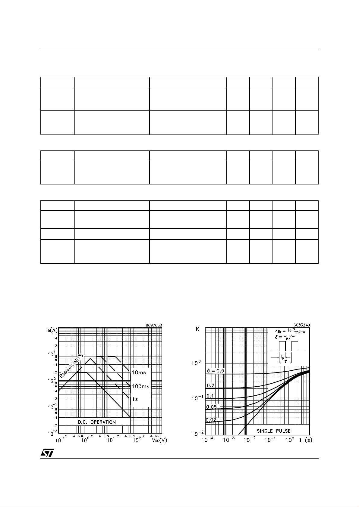
Saf e Operating Are a
Thermal Impedance Junction-lead
3/8
 Loading...