

SGS Thomson Microelectronics STN2NE06 Datasheet
STN2NE06
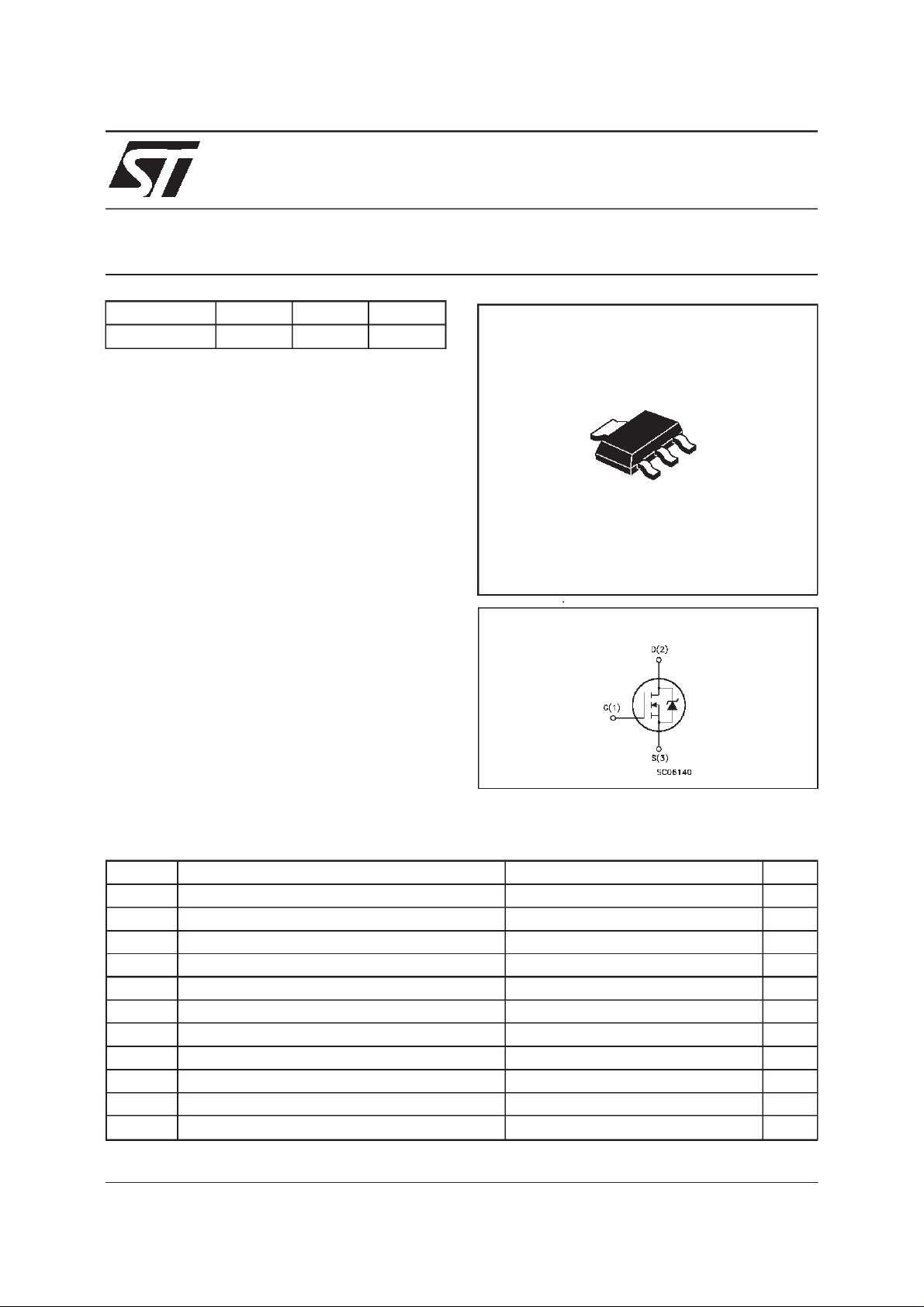
N-CHANNEL 60V - 0.18Ω - 2A - SOT-223
STripFET POWER MOSFET
TYPE V
DSS
R
DS(on)
I
D
ST N2NE06 60 V < 0 . 25 Ω 2A
■ TYPICALR
■ EXCEPTIONALdv/dtCAPABILITY
■ AVALANCHERUGGEDTECHNOLOGY
■ 100 % AVALANCHETESTED
■ APPLICATIONORIENTED
DS(on)
= 0.18 Ω
CHARACTERIZATION
DESCRIPTION
This Power Mosfet is the latest development of
STMicroelectronics unique ”Single Feature
Size” stip-based process. The resulting transi-
stor shows extremely high packing density forlow
on-resistance, rugged avalanche characteristics
and less critical alignment steps therefore a remarkablemanufacturingreproducibility.
APPLICATIONS
■ DC MOTOR CONTROL(DISK DRIVES,etc.)
■ DC-DC& DC-AC CONVERTERS
■ SYNCHRONOUSRECTIFICATION
2
3
2
1
SOT-223
INTERNAL SCHEMATIC DIAGRAM
ABSOLUTE MAXIMUM RATINGS
Symbol Parameter Value Uni t
V
V
V
I
DM
P
dv/ dt (
T
(•) Pulse width limited by safe operating area (1)ISD≤ 8 A, di/dt ≤ 200 A/µs, VDD≤ V
April 1999
Drain-source Voltage (VGS=0) 60 V
DS
Drain- gate Volt age (RGS=20kΩ)60V
DGR
Gate-source Voltage ± 20 V
GS
I
Drain Current (continuous ) at Tc=25oC2A
D
I
Drain Current (continuous ) at Tc=100oC1.3A
D
(•) Drain Current (pulsed) 8 A
Total Dissipation at Tc=25oC2.5W
tot
Derat ing Factor 0.02 W/
1 ) Peak Diode Recovery voltage s lope 6 V/ns
Sto rage Temperature -65 t o 150
stg
T
Max. Operating Junct ion Temperat ur e 150
j
(BR)DSS,Tj≤TJMAX
o
C
o
C
o
C
1/8
STN2NE06
THERMAL DATA
R
thj-pcb
R
thj-amb
T
AVALANCHE CHARACTERISTICS
Symbol Parameter Max Value Unit
I
AR
E
Ther mal Resistanc e Junct ion-PC Board Max
Ther mal Resistanc e Junct ion-ambient Max
(Surface Mounted)
Maximum Lead Te m perature For Soldering Purpos e
l
Avalanche Current, Repetitive or Not-Repetitive
(pulse width limited by T
Single Pulse Avalanche Energy
AS
(starting T
=25oC, ID=IAR,VDD=25V)
j
max)
j
50
60
260
2A
20 mJ
o
C/W
o
C/W
o
C
ELECTRICAL CHARACTERISTICS
=25oC unless otherwisespecified)
(T
case
OFF
Symbol Parameter Test Condit ions Min. Typ. Max. Unit
V
(BR)DSS
Drain-source
ID=250µAVGS=0 60 V
Break dow n Voltage
I
DSS
I
GSS
Zero Gate Voltage
Drain Current (V
GS
Gat e- bod y Leakage
Current (V
DS
=0)
=0)
V
=MaxRating
DS
=MaxRating Tc= 125oC
V
DS
V
=± 20 V
GS
1
10
100 nA
±
ON(∗)
Symbol Parameter Test Condit ions Min. Typ. Max. Unit
V
GS(th)
R
DS(on)
Gate Threshold Voltage VDS=VGSID= 250 µA 234V
Sta t ic Dr ain -s ource On
VGS=10V ID= 1 A 0.18 0.25
Resistance
I
D(on)
On State Drain Current VDS>I
D(on)xRDS(on )max
2A
VGS=10V
DYNAMIC
Symbol Parameter Test Condit ions Min. Typ. Max. Unit
g
(∗)Forward
fs
Tr ansc on duc tance
C
C
C
Input C apac i t ance
iss
Out put Capacitanc e
oss
Reverse T r ansfer
rss
Capacit a nc e
VDS>I
D(on)xRDS(on )maxID
=1A 1.8 S
VDS=25V f=1MHz VGS= 0 V 310
45
12.5
420
61
17
µ
µA
Ω
pF
pF
pF
A
2/8
STN2NE06
ELECTRICAL CHARACTERISTICS
(continued)
SWITCHINGON
Symbol Parameter Test Condit ions Min. Typ. Max. Unit
t
d(on)
Q
Q
Q
Turn-on Time
Rise T i me
t
r
Tot al G at e Char ge
g
Gat e- Source Charge
gs
Gate-Drain Charge
gd
VDD=30V ID=1A
R
=4.7
G
Ω
VGS=10V
9
10
VDD=40V ID=2A VGS=10V 12
5.1
2.7
13
13.5
17
7
4
SWITCHINGOFF
Symbol Parameter Test Condit ions Min. Typ. Max. Unit
t
r(Voff)
t
t
Off-volt age R ise Time
Fall T ime
f
Cross-over T ime
c
VDD=48V ID=2A
=4.7ΩVGS=10V
R
G
4.5
5
12
6
7
16
SOURCEDRAINDIODE
Symbol Parameter Test Condit ions Min. Typ. Max. Unit
I
SD
I
SDM
V
SD
t
Q
I
RRM
(∗) Pulsed: Pulse duration = 300µs, duty cycle 1.5 %
(•) Pulse width limited by safe operating area
Source-drain Current
(•)
Source-drain Current
2
8
(pulsed)
(∗)ForwardOnVoltage ISD=2A VGS=0 1.2 V
Reverse Re covery
rr
Time
Reverse Re covery
rr
ISD= 2 A di/dt = 100 A/µs
=30V Tj=150oC
V
DD
40
50
Charge
Reverse Re covery
2.5
Current
ns
ns
nC
nC
nC
ns
ns
ns
A
A
ns
nC
Α
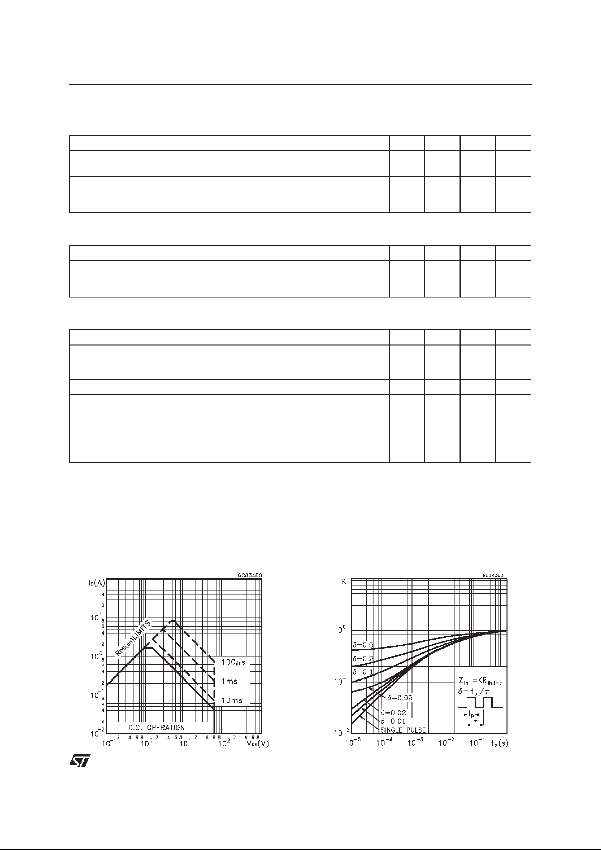
SafeOperating Area ThermalImpedance
3/8
 Loading...