

SGS Thomson Microelectronics STN2N06 Datasheet
N - CHANNEL ENHANCEMENT MODE
TYPE V
DSS
STN2N06 60 V < 0.250 Ω 2 A
R
DS(on)
I
D
CONT
STN2N06
POWER MOS TRANSISTOR
ADVANCE DATA
■ TYPICAL R
■ AVALANCHE RUGGED TECHNOLOGY
■ SOT-223 CAN BE WAVE OR REFLO W
DS(on)
= 0.21 Ω
SOLDERED
■ AVAILABLE IN TAPE AND REEL ON
REQUEST
o
■ 150
■ APPLICATION ORIENTED
C OPERATING TEMPERATURE
CHARACTERIZATION
APPLICATIONS
■ HARD DISK DRIVERS
■ SMALL MOTOR CURRENT SENS E
CIRCUITS
■ DC-DC CONVERTE RS A ND PO WER
SUPPLIES
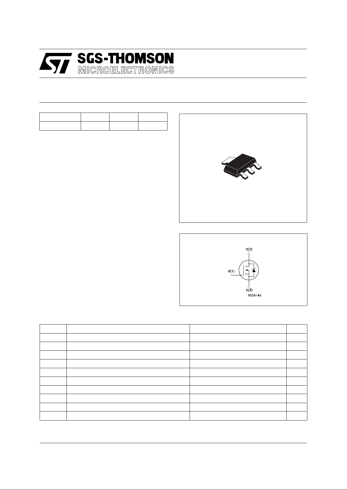
2
3
2
1
SOT-223
INTERNAL SCHEMATIC DIAGRAM
ABSOL UT E MAXIMU M RATINGS
Symbol Parameter Value Unit
V
V
V
I
D
I
D
I
DM
P
T
(•) Pulse width limited by safe operating area (*) Limited by package
March 1996
Drain-source Voltage (VGS = 0) 60 V
DS
Drain- gate Voltage (RGS = 20 kΩ)60V
DGR
Gate-source Voltage ± 20 V
GS
(*) Drain Current (continuous) at Tc = 25 oC2A
(*) Drain Current (continuous) at Tc = 100 oC 1.3 A
(•) Drain Current (pulsed) 8 A
Total Dissipation at Tc = 25 oC 2.7 W
tot
Derating Factor 0.022 W/
Storage Temperature -65 to 150
stg
T
Max. Operating Junction Temperature 150
j
o
C
o
C
o
C
1/5
STN2N06
THERMAL DATA
R
thj-pcb
R
thj-amb
Thermal Resistance Junction-PC Board Max
Thermal Resistance Junction-ambient Max
(Surface Mounted)
T
Maximum Lead Temperature For Soldering Purpose
l
AVALANCHE CHARACTERI S TICS
Symbol Parameter Max Value Unit
I
AR
E
E
I
AR
Avalanche Current, Repetitive or Not-Repetitive
(pulse width limited by T
Single Pulse Avalanche Energy
AS
(starting T
Repetitive Avalanche Energy
AR
= 25 oC, ID = IAR, V
j
(pulse width limited by T
max, δ < 1%)
j
DD
max, δ < 1%)
j
Avalanche Current, Repetitive or Not-Repetitive
(T
= 100 oC, pulse width limited by Tj max, δ < 1%)
c
= 25 V)
46
60
260
2A
40 mJ
10 mJ
1.3 A
o
C/W
o
C/W
o
C
ELECTRICAL CHARACTERISTICS (T
= 25 oC unless otherwise specified)
case
OFF
Symbol Parameter Test Conditions Min. Typ. Max. Unit
V
(BR)DSS
Drain-source
ID = 250 µA V
= 0 60 V
GS
Breakdown Voltage
I
DSS
I
GSS
Zero Gate Voltage
Drain Current (V
GS
Gate-body Leakage
Current (V
DS
= 0)
= 0)
= Max Rating
V
DS
V
= Max Rating x 0.8 Tc = 125 oC
DS
= ± 20 V ± 100 nA
V
GS
250
1000µAµA
ON (∗)
Symbol Parameter Test Conditions Min. Typ. Max. Unit
V
GS(th)
R
DS(on)
I
D(on)
Gate Threshold Voltage V
Static Drain-source On
Resistance
= VGS ID = 250 µA 234V
DS
VGS = 10 V ID = 1 A
V
= 10 V ID = 1 A Tc = 100oC
GS
On State Drain Current VDS > I
V
= 10 V
GS
D(on)
x R
DS(on)max
0.21 0.25
0.5
2A
DYNAMIC
Symbol Parameter Test Conditions Min. Typ. Max. Unit
g
(∗) Forward
fs
Transconductance
C
C
C
Input Capacitance
iss
Output Capacitance
oss
Reverse Transfer
rss
Capacitance
VDS > I
V
DS
x R
D(on)
DS(on)max
= 25 V f = 1 MHz V
ID = 1 A 0.8 1.5 S
= 0 V 260
GS
90
30
340
120
40
Ω
Ω
pF
pF
pF
2/5
 Loading...