

STN1N20
N - CHANNEL 200V - 1.2
TYPE V
DSS
ST N1N2 0 200 V < 1.5 Ω 1A
■ TYPICALR
■ AVALANCHERUGGEDTECHNOLOGY
■ SOT-223CAN BE WAVEOR REFLOW
DS(on)
= 1.2 Ω
SOLDERED
■ AVAILABLEIN TAPEAND REELON
REQUEST
o
■ 150
■ APPLICATIONORIENTED
C OPERATINGTEMPERATURE
CHARACTERIZATION
APPLICATIONS
■ HARDDISK DRIVERS
■ SMALLMOTORCURRENT SENSE
CIRCUITS
■ DC-DCCONVERTERS AND POWER
SUPPLIES
R
DS(on)
I
CONT
D
Ω
- 1A - SOT-223
POWER MOS TRANSISTOR
PRELIMINARY DATA
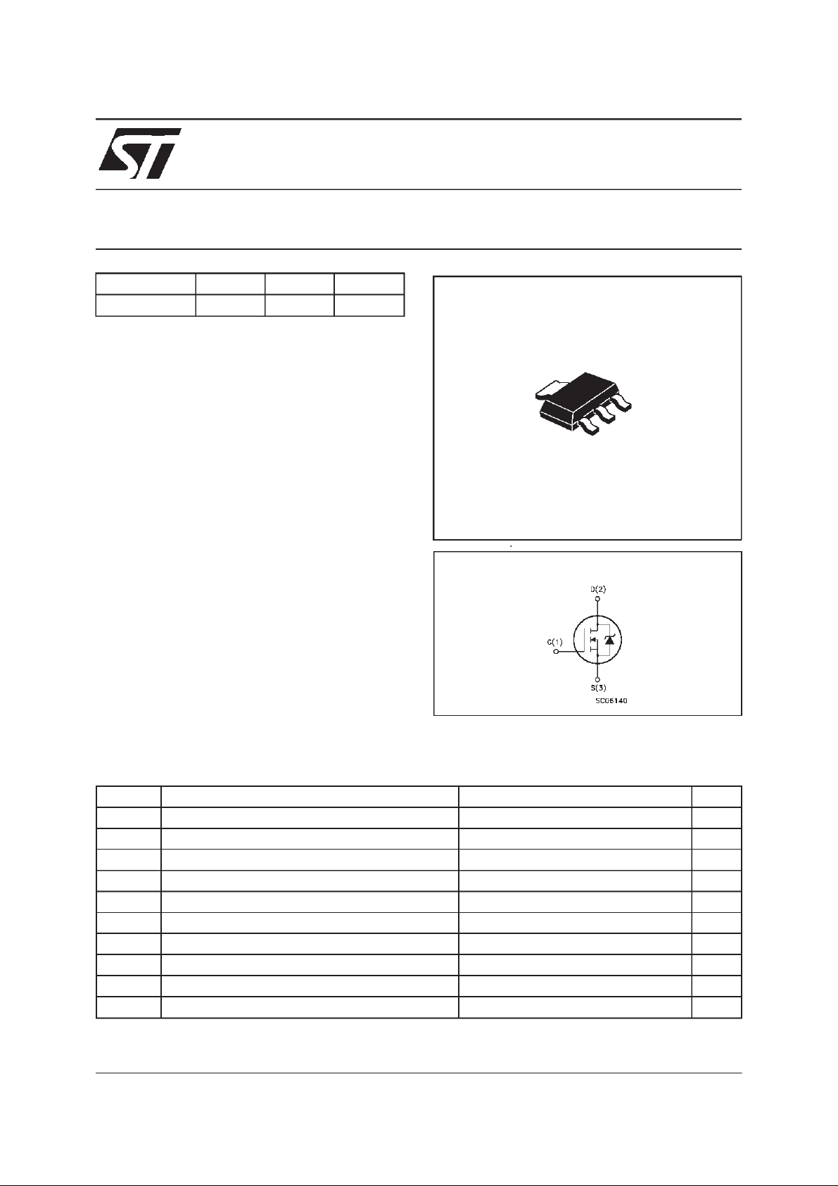
2
3
2
1
SOT-223
INTERNAL SCHEMATIC DIAGRAM
ABSOLUTE MAXIMUM RATINGS
Symb o l Parameter Value Unit
V
V
V
I
D
I
D
I
DM
P
T
(•) Pulse width limited by safeoperating area (*) Limited by package
September 1999
Drain-source Voltage (VGS= 0) 200 V
DS
Drain- gate Volt ag e (RGS=20kΩ) 200 V
DGR
Gate-s ource Voltage
GS
20 V
±
(*) Drain Current (co ntinuous) at Tc=25oC1A
(*) Drain Current (co ntinuous) at Tc=100oC 0.6 A
(•) Drain Curr ent (pu lsed) 4 A
Tot al Di ss i pat ion at Tc=25oC 2.9 W
tot
Derat ing Factor 0.023 W/
Sto rage Tem per at ur e -65 t o 15 0
stg
T
Max. Operat ing Junct ion T emperat ure 150
j
o
C
o
C
o
C
1/6
STN1N20
THERMAL DATA
R
thj-pcb
R
thj-amb
T
AVALANCHE CHARACTERISTICS
Symbol Parameter Max V alue Unit
I
AR
E
Ther mal Resistanc e Junct ion-PC B oa rd Max
Ther mal Resistanc e Junct ion-ambient Max
(Surface Mounted)
Maximum Lead Te m perature For Soldering Purpos e
l
Avalanche C urrent, R epetitive or Not-Repetitive
(pulse width limited by T
Single P ul s e Avalan c he Energy
AS
(starting T
=25oC, ID=IAR,VDD=25V)
j
max)
j
43
60
260
1A
10 mJ
o
C/W
o
C/W
o
C
ELECTRICAL CHARACTERISTICS
=25oC unless otherwisespecified)
(T
case
OFF
Symbol Parameter Test Conditions Min. Typ. M ax. Unit
V
(BR)DSS
Drain-source
ID=250µAVGS= 0 200 V
Break dow n Voltage
I
DSS
I
GSS
Zero Gate Voltage
Drain Current (V
GS
Gat e- bod y L eak ag e
Current (V
DS
=0)
=0)
V
=MaxRating
DS
=MaxRating Tc= 125oC
V
DS
V
=± 20 V
GS
10
100
100 nA
±
ON(∗)
Symbol Parameter Test Conditions Min. Typ. M ax. Unit
V
GS(th)
R
DS(on)
Gate Threshold Voltage VDS=VGSID= 250 µ A 234V
Sta t ic Drain -s ource On
VGS=10V ID= 0.5 A 1.2 1.5
Resistance
I
D(on)
On State Drain Current VDS>I
D(on)xRDS(on )max
1A
VGS=10V
DYNAMIC
Symbol Parameter Test Conditions Min. Typ. M ax. Unit
g
(∗)Forward
fs
Tr ansc on duc tance
C
C
C
Input Capac i t anc e
iss
Out put Capacitanc e
oss
Reverse Tr ansfer
rss
Capacit a nc e
VDS>I
D(on)xRDS(on )maxID
=0.5A 0.3 0.7 S
VDS=25V f=1MHz VGS= 0 V 290
50
10
400
70
15
µ
µA
Ω
pF
pF
pF
A
2/6
 Loading...