■ LINEARPOWER AMPLIFIER
■ 890-915MHz
■ 12.5 VOLTS
■ INPUT/OUTPUT50 OHMS
■ POUT = 16 W MIN.
■ GAIN = 42 dB MIN.
DESCRIPTION
The STM915-16 is a linear power module
designed for 12.5 V applications in GSM Cellular
Radio Systems. The STM915-16 uses gold
metallized transistors with diffused emitter ballast
resistors for high linearity Class AB operation.
STM915-16
RF POWER MODULE
GSM MOBILE APPLICATIONS
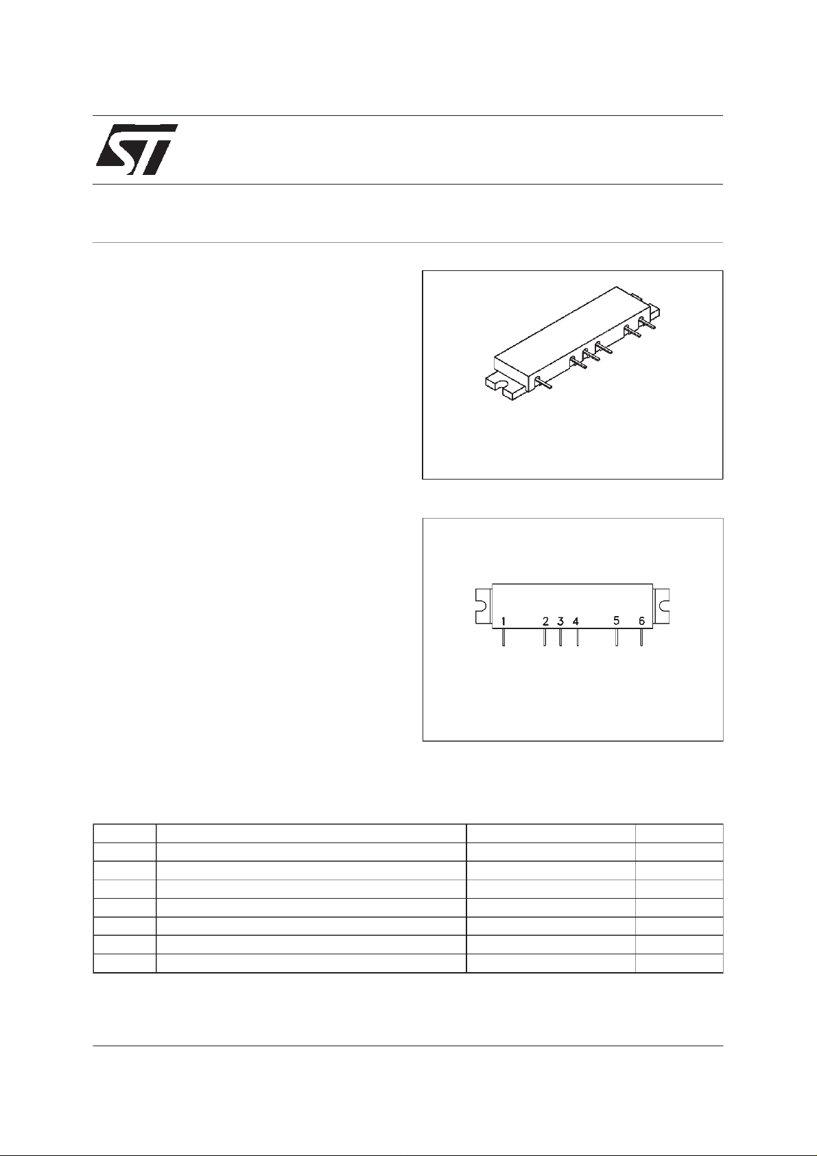
CASE H100
ORDER CODE BRANDING
STM915-16 STM915-16
PIN CONNECTION
1 RF Input 4 8.0 Vdc
2 8.0Vdc 5 12.5 Vdc
3 12.5 Vdc 6 RF Output
ABSOLUTE MAXIMUM RATINGS (T
Symb o l Para meter Val u e Unit
V
S2,VS4
V
S1,VS3
V
CONTROL
P
P
OUT
T
T
Note1: Pulse Width= 577 µsec.
June 1999
DC Supply V olt ag e (RF appl ied / No RF ap plied ) 15.6/ 30.0 Vdc
DC Supply V olt ag e 8.5 Vdc
DC Contr o l Voltage 4.5 Vdc
RF I nput P ower (P
IN
1
RF O utpu t Power (VS2,VS4=12.5V) 20 W
Sto rage Tempe r ature - 30 to + 100
STG
Oper ating Case Tem peratu re - 30 to + 100
C
Repetition rate = 4.6 msec.
OUT
=25oC)
case
≤ 17 W)
3.0 mW
o
C
o
C
1/7

STM915-16
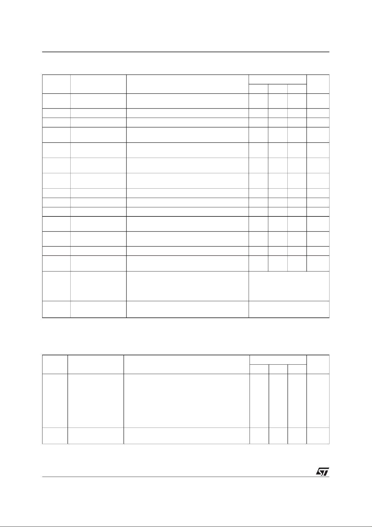
ELECTRICALSPECIFICATIONS(T
case
25°C, V
=
S1
, V
S3
=
8.0 Vdc; V
S2
, V
S4
=
12.5 Vdc)
Symbol Parame ter Test Condi tio ns Value Unit
Min. Typ. Max.
BW Frequ e nc y Range 890 915 MHz
P
I
I
I
Output Power
OUT
η
Efficiency
Leakag e Curr en t ,
Q1
V
S1,VS2
Bias Curre nt,
Q2
V
S3
Quiescent Current ,
Q3
V
S4
Contr ol Dynamic
Range
Isol at i on
H Harmonics
VSWR
V
CONT
I
CONT
Input VS WR
IN
Contr ol Volt a ge 0 4.0 Vdc
Contr ol Current 1.0 2.0 mA
1,2
1, 2
3
1, 2
1,2
V
P
V
V
V
V
V
P
P
=
4.0 Vdc PIN= 1mW
CONT
16 W
=
OUT
=
0Vdc PIN=
CONT
=
0Vdc PIN=
CONT
=
0Vdc PIN=
CONT
=
0to4.0V
CONT
=
0Vdc V
CONT
=
42 dBm reference
OUT
=
+13dBmto+42dBm
OUT
S2, S4
1mW
1mW
1mW
=
0 to 15. 6V
16 W
35 41 %
0.5 2.0 mA
140 150 mA
200 250 mA
56 dB
−14 d Bm
−45 dBc
2.0:1
T
r
Notes: 1) P
2) PulseWidth
Repetition rate
Rise Time
Noise Power 30 KHz B and width, 20 MH z ab ove f
Stab ilit y
Load Mi s match
1.0mW adjust V
IN =
1, 2, 4
1, 2
CONTROL
577 µsec. 4)Trmeasured at 1% to81% ofP
=
4.6 msec.
=
P
=
+13 to +42 dBm
OUT
P
=
+13dBmto+42dBmCW
OUT
P
= − 14 to +42 dBm
OUT
=
V
S2,VS4
Load VSWR
10.8to15.6V
=
6:1 Sourc e VS WR= 3:1
All phase angles T
1,2
VSWR= 10:1 Al l p hase angles
=
15.6Vdc P
V
forspecified P
OUT
OUT
.3)P
=
− 20 to + 6 0°C
C
= 16 W
(Reference) =42 dBm
OUT
1.0 µSec
0
−70 −65 dBm
AllSpurious outputs more
than 60dB below carrier
No Degradationin Output
Power
OUT
in watts
REF. 1014655E
GSM SPECIFIC TESTS
Symbol Parameter Test Conditi ons Value Unit
Min. Typ. Max.
AM/AM Conversion
Gain
PIN= fo(0 dBm)+[fo+200kHz(−40 dBm )]
V
CONT RO L
P
OUT
P
OUT(fo
P
OUT(fo
adjusted for
= 13, 30, 42 dBm
+200kHz)
− 20 0 k Hz )
− 40
− 45
dBc
dBc
2/7
AM/PM Conversion
= +13 t o + 42 dBm
P
OUT
varied +/− .5 dB
P
IN
4 °/dB

MODULEDCAND TEST FIXTURE CONFIGURATION
STM915-16
REF. 1015959E
3/7
 Loading...