

SGS Thomson Microelectronics STM2DPFS30L Datasheet
P - CHANNEL 30V - 0.145Ω - 2A MiniS0-8
STripFET
MAIN PRODUCT CHARACTERISTICS
MOSFET
SCHOTTKY
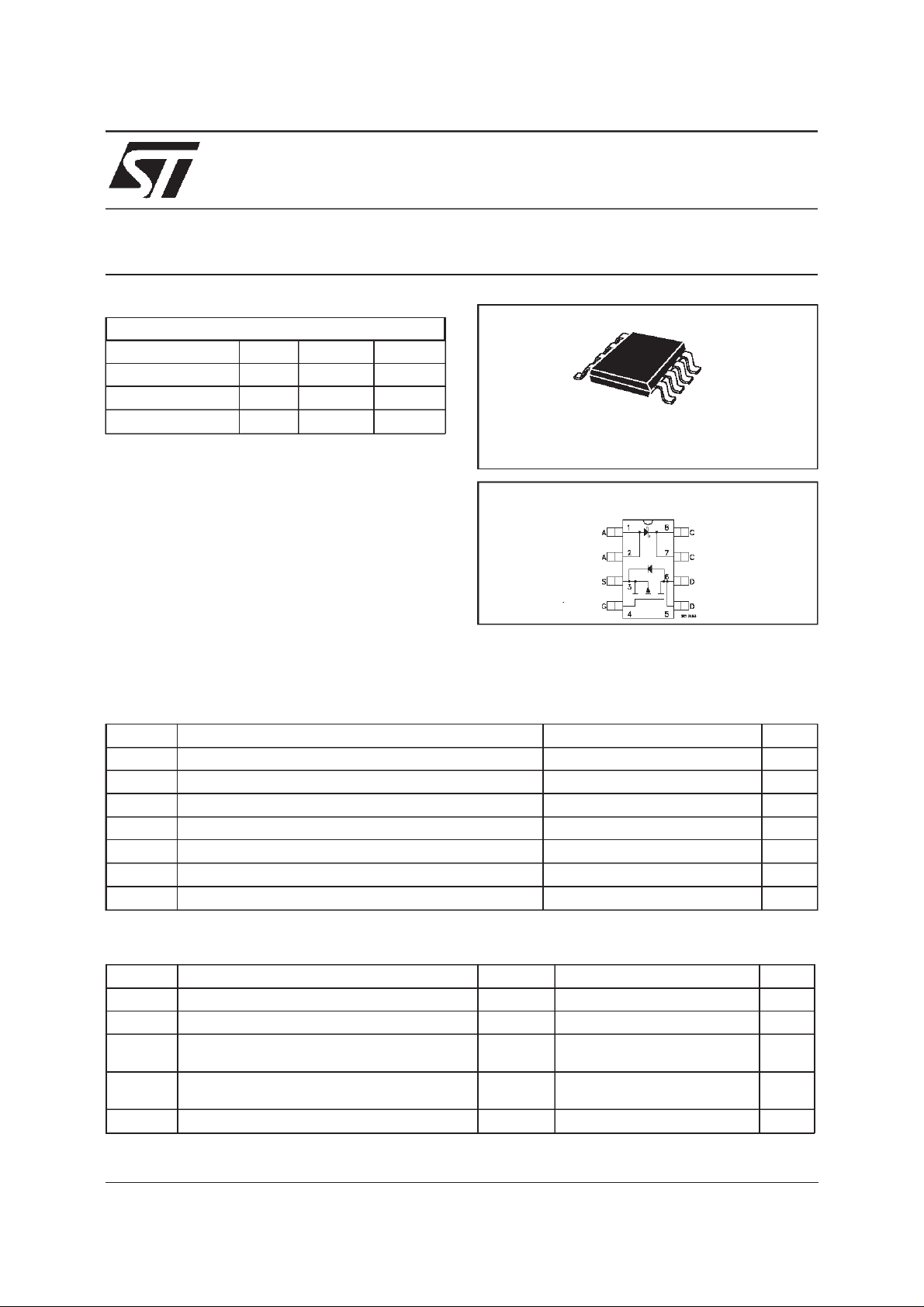
DESCRIPTION:
This product ass oci at es the latest low volta ge
StripFET
Schot tky diode. Such configura t ion is extr em ely
versa ti le in i mplement ing a large v ariet y of DC- DC
converters for print ers, portable equipm ent , and
cellular phones.
New MiniSO -8 pack age features:
■ Half footprintareaversus standardSO-8,for
■ Extremelylow profile,ideal for low thickness
in p-chann el ver si on to a low drop
applicationwhere minimum circuitboard
space is necessary.
equipment.
MOSFET PLUS SCHOTTKY RECTIFIER
V
DSS
30V <0. 165 Ω 2A
I
F(AV)
1A 40V 0.55V
R
DS(on)
V
RRM
V
F(MAX)
I
D
STM2DPFS30L
PRELIMINARY DATA
MiniSO-8
INTERNAL SCHEMATIC DIAGRAM
MOSFETABSOLUTE MAXIMUM RATINGS
Symbol Parameter Value Unit
V
V
V
I
DM
P
Drain-source V olt a ge (VGS=0) 30 V
DS
Drain- gate Vol ta ge (RGS=20kΩ)30V
DGR
Gat e- sour c e Volt age ± 20 V
GS
I
Drain Current ( c ont i nuous) at Tc=25oC2A
D
I
Drain Current ( c ont i nuous) at Tc= 100oC1.3A
D
(•) Drain Current (pulsed) 8 A
Tot al Dissip ation at Tc=25oC1.25W
tot
SCHOTTKY ABSOLUTE MAXIMUM RATINGS
Symbol Parameter Valu e Unit
V
I
F(RMS)
I
F ( AV)
I
FSM
dv/d t Crit i c al Rat e Of Rise Of Re ver se V olt age 10000 V/µs
(•) Pulse width limited by safe operating area
Note:For the P-CHANNEL MOSFET actual polarity of voltagesand current has to be reversed
July 1999
Repetitive P eak Revers e Vol t age 40 V
RRM
RMS Forwa r d Current 2 A
Aver ag e F orw ar d Current Ta=60oC
δ =0.5
Surge Non Repetitive Forward C urrent tp= 10 ms
Sinusoidal
1.2 A
5.5 A
1/6
STM2DPFS30L
THERMAL DATA
R
thj-amb
T
T
(*)Mounted on a 1 in
(*) Thermal Resist ance Juncti on- ambient MOS F E T
Sto rage Tem perature Range Maximum
stg
Junct ion T em per ature
j
2
pad of 2oz Cu in FR-4board
100
-65 to 150
150
o
C/W
o
o
C
C
MOSFETELECTRICAL CHARACTERISTICS
=25oC unless otherwisespecified)
(T
case
OFF
Symbol Parameter Test Conditions Min. Typ. Max. Unit
V
(BR)DSS
Drain-source
ID=250µAVGS=0 30 V
Break dow n Voltage
I
DSS
I
GSS
Zero Gate Voltage
Drain Current (V
GS
=0)
Gat e- bod y Leakage
Current (V
DS
=0)
V
=MaxRating
DS
=MaxRating Tc= 125oC
V
DS
= ± 20 V ± 100 nA
V
GS
1
10
ON(∗)
Symbol Parameter Test Conditions Min. Typ. Max. Unit
V
GS(th)
R
DS(on)
I
D(on)
Gate Threshold Voltage VDS=VGSID= 250 µA11.72.5V
Sta t ic Dr ain-source On
Resistance
VGS=10V ID=1A
=4.5V ID=1A
V
GS
On State Drain Current VDS>I
D(on)xRDS(on)max
0.145
0.18
2A
0.165
0.2
VGS=10V
DYNAMIC
Symbol Parameter Test Conditions Min. Typ. Max. Unit
g
(∗)Forward
fs
Tr ansc on duc tance
C
C
C
Input Capaci t ance
iss
Out put Capac it ance
oss
Reverse Transfer
rss
Capacit a nc e
VDS>I
D(on)xRDS(on)maxID
=1 A 2 S
VDS=25V f=1MHz VGS= 0 510
170
55
660
220
72
µA
µA
Ω
pF
pF
pF
2/6
 Loading...