

SGS Thomson Microelectronics STLVDS9637BDR, STLVDS9637BD, STLVDS3486BTR, STLVDS3486BD, STLVDS3486BDR Datasheet
...
1/13May 2003
■ MEETS OR EXCEEDS THE
REQUIREMENTS OF ANSI TIA/EIA-644
STANDARD
■ OPERATES WITH A SINGLE 3.3V SUPPLY
■ DESIGNED FOR SIGNA LING RATE UP TO
400Mbps
■ DIFFERENTIAL INPUT THRESHOLDS
±100mV MAX
■ TYPICAL PROPAGATION DELAY TIME OF
2.5ns
■ POWER DISSIPATION 60mW TYPICAL PER
RECEIVER AT 200MHz
■ LOW VOLATGE TTL (LVTTL) LOGIC
OUTPUT LEVELS
■ PIN COMPATIBLE WITH THE AM26LS32,
SN65LVD32
■ OPEN CIRCUIT FAIL SAFE
■ ESD PROTECTION:
7KV RECEIVER PINS
3KV ALL PINS VS GND
DESCRIPTION
The STLVDS32 is a differential line receiver that
implements the electrical characteristics of low
voltage differential signaling (LVDS). This
signaling technique lowers the output voltage
levels of 5V differential standard levels (such as
TIA/EIA-422B) to reduce t he power, increase the
switching speeds and allow operationswith a 3.3V
supply rail. This differential receiver provides a
valid logical output s tate with a 3.3V supply rail. It
also provides a valid logi cal output st ate with a
±100mV differential input voltage within the input
common mode voltage range. The input common
mode voltage allows 1V of ground potential
difference between two LVDS nodes .
The intended application of this device and
signalling technique is both point-to-point and
multidrop data transmission over controlled
impedance media approximately 100Ω.The
transmission media may be printed circuit board
traces, backplanes or cables. The ultim ate rat e
and distance of data transfer depend upon the
attenuation characte ristics of the media and noise
coupling to the environment.
The STLVDS32 v ers ion is characterized for
operation from -4 0°C to 85°C.
ORDERING CODES
Type
Temperature
Range
Package Comments
STLVDS32BD -40 to 85 °C SO-16 (Tube) 50parts per tube / 20tube per box
STLVDS32BDR -40 to 85 °C SO-16 (Tape & Reel) 2500 parts per reel
STLVDS32BTR -40 to 85 °C TSSOP16 (Tape & Reel) 2500 parts per reel
STLVDS32
HIGH SPEED
DIFFERENTIAL LINE RECEIVERS
SOP TSSOP
STLVDS32
2/13
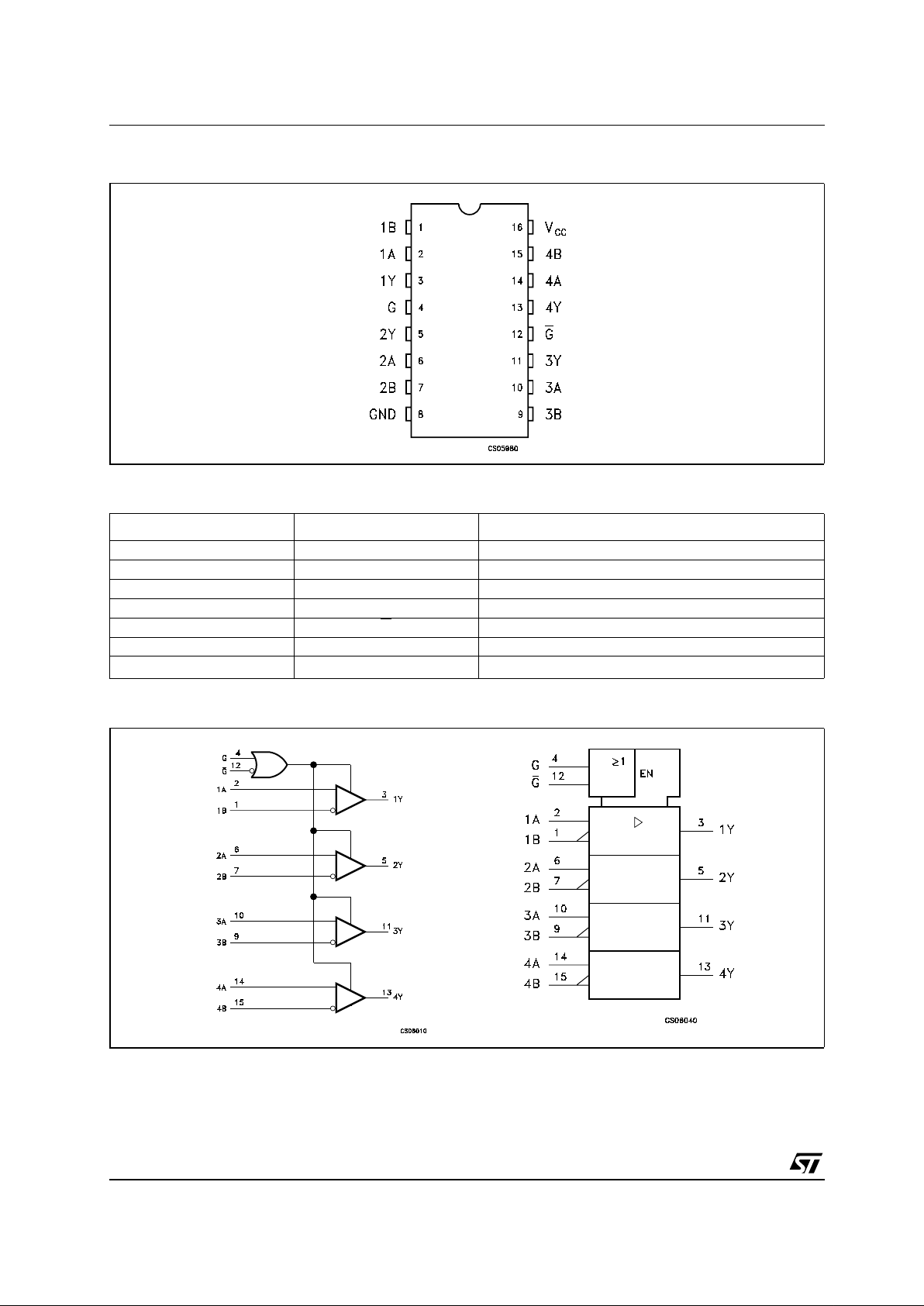
PIN CONFIGURATION
PIN DESCRIPTION
LOGIC DIAGRAM AND LOGIC SYMBOL
PlN N° SYMBOL NAME AND FUNCTION
2, 6, 10, 14 1A to 4A Receiver Inputs
1, 7, 9, 15 1B to 4B Negated Receiver Inputs
3, 5, 11, 13 1Y to 4Y Receiver Outputs
4 G Enable
12 G
Enable
8 GND Ground
16
V
CC
Supply Voltage
STLVDS32
3/13
TRUTH TABLE
L = Low level, H = High Level, X = Don’t care, Z = High Impedance,? = Indeterminate
ABSOLUTE MAXIMUM RATINGS
Absolute Maximum Ratings are those values beyond which damage to the device may occur. Functional operation under these condition is
not implied.
Note 1: All voltages except differential I/O bus voltage, are with respect to the network ground terminal.
RECOMMENDED OPERATING CONDITIONS
DIFFERENTIAL INPUTS ENABLES OUTPUT
A, B G G
Y
V
ID
≥ 100mV
HX H
XL H
-100mV < V
ID
< 100mV
HX ?
XL ?
V
ID
≤ -100mV
HX L
XL L
XLHZ
OPEN
HX H
XL H
Symbol Parameter Value Unit
V
CC
Supply Voltage (Note 1)
-0.5 to 4.6 V
V
I
Input Voltage -0.5 to (VCC+ 0.5)
V
V
I
Input Voltage (A or B inputs)
-0.5 to 4.6 V
ESD
Human Body Model Pins Receivers 7
KV
All Pins vs GND 3
T
stg
Storage Temperature Range
-65 to +150 °C
Symbol Parameter Min. Typ. Max. Unit
V
CC
Supply Voltage 3.0 3.3 3.6 V
V
IH
HIGH Level Input Voltage (ENABLE) 2.0 V
V
IL
LOW Level Input Voltage (ENABLE) 0.8 V
|V
ID
| Magnitude of Differential Input Voltage 0.1 0.6 V
V
IC
Common Mode Input Voltage 0.5|VID| 2.4-0.5|VID|V
V
CC
- 0.8
T
A
Operating Temperature Range
-40
85
°C
STLVDS32
4/13
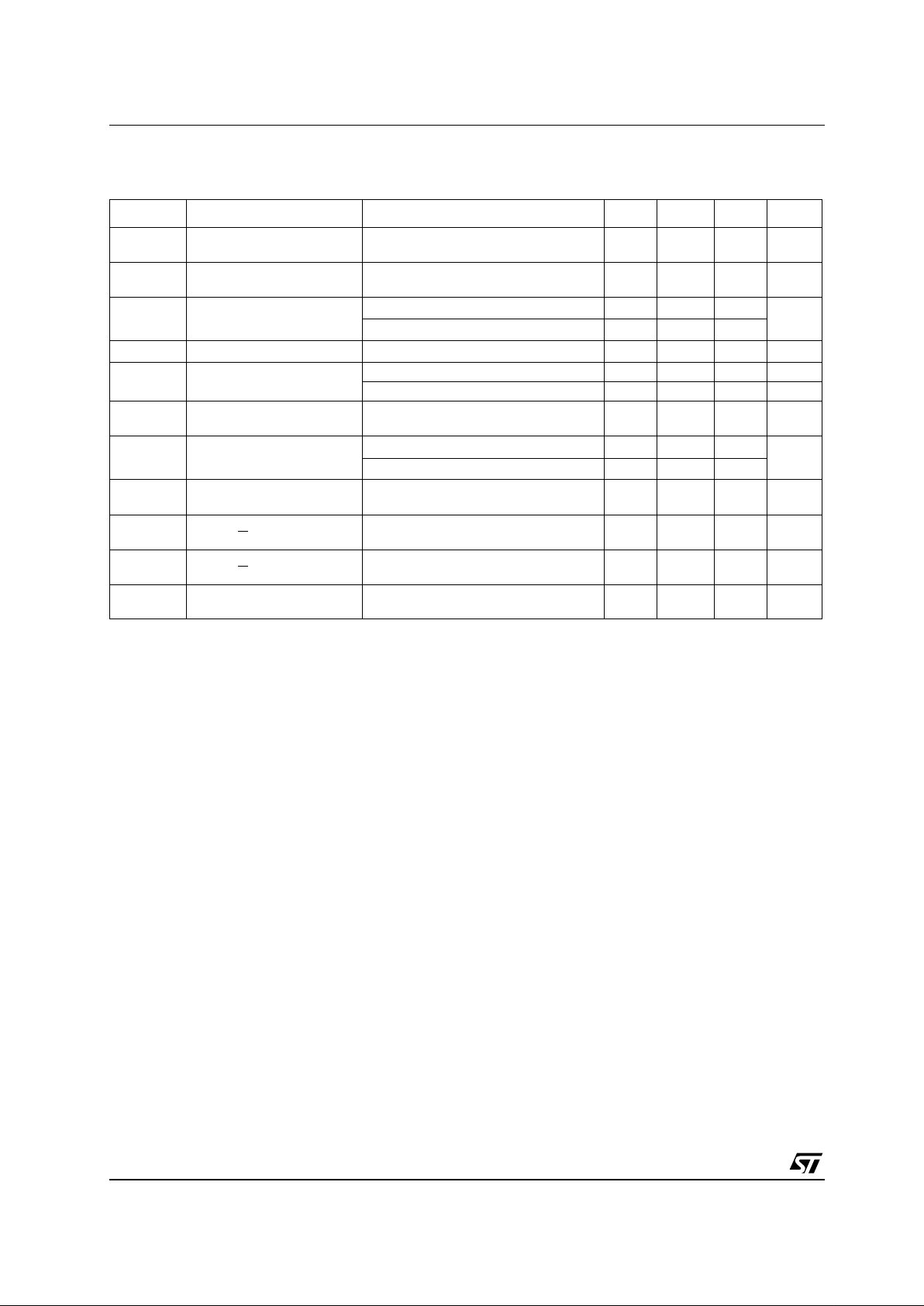
ELECTRICAL CHARACTERISTICS (Over recommended operating conditions unless otherwise noted.
All typical values are at T
A
= 25°C, and VCC=3.3V)
Symbol Parameter Test Conditions Min. Typ. Max. Unit
V
ITH+
Positive Going Differential
Input Voltage Threshold
100 mV
V
ITH-
Negative Going Differential
Input Voltage Threshold
-100 mV
V
OH
High Level Output Voltage IOH= -8mA 2.4 V
I
OH
=-4mA 2.8
V
OL
Low Level Output Voltage IOH= 8mA 0.4 V
I
CC
Supply Current for
STLVDS32, STLVDS3486
Enabled, No Load 10 18 mA
Disabled 0.25 0.5 mA
I
CC
Supply Current for
STLVDS9637
No Load 4 10 mA
I
I
Input Current (A or B inputs) VI= 0V -2 -10 -20 µA
V
I
= 2.4V -1.2 -3
I
I(OFF)
Power off Input Current (A
or B inputs)
VCC=0 VI= 3.6V 10 20 µA
I
IH
High Level Input Current
(EN, G, G
or Inputs)
V
IH
=2V 10 µA
I
IL
Low Level Input Current
(EN, G, G
or Inputs)
V
IL
= 0.8V 10 µA
I
OZ
High Impedance Output
Current
VO= 0 or V
CC
± 10 µA
 Loading...