

SGS Thomson Microelectronics STLVDS47BTR, STLVDS47BDR, STLVDS47BD Datasheet
3V LVDS Q UAD CMOS DIFFERENTIAL LINE DRIVER
■ >400 MBPS (200MHZ) SWITCHING RATES
■ FLOW-THROUGH PINOUTSIMPLIFIES PCB
LAYOUT
■ 300ps (MAX.) DIFFERENTIAL SKEW
■ 1.8 ns (TYP.) PROPAGATION DELAY
■ 3.3V POWER SUPPLY DESIGN
■ ±350 mV DIFFERENTIAL SIGNALING
■ LOW POWER DISSIPATION (3.5mW AT 3.3V
STATIC IN TRISTATE)
■ INTEROPERABLEWITHEXISTING5V LVDS
RECEIVERS
■ HIGH IMPEDANCE ON LVDS OUTPUT ON
POWER DOWN
■ CONFORMS TO TIA/EIA-644 LVDS
STANDARD
■ INDUSTRIAL OPERATING TEMPERATURE
RANGE (-40 °C TO +85 °C)
■ AVAILABLE IN SURFACE MOUNT (S OIC)
AND LOW PROFILE TSSOP PACKAGE
DESCRIPTION
The STLVDS47 is a quad CMOS flow-through
differential line driver designed for applications
requiring ultra low power dissipation and high data
rate. The device is designed to support data rates
in excess of 400Mbp s (200 MHz) utilizing Low
Voltage Differential Signaling (LVDS) techology.
The STLVDS47 accepts low voltage TTL/CMOS
input levels and translates them to low voltage
STLVDS47
SO-16 TSSOP
(350 mV) differential output signals. In addition,
the driver support a TRI-STATE function that may
be used to disable the output stage, disabling the
load current, and thus dropping the device to an
ultra low idle power state of 1.3mW typical. The
STLVDS47 has a flow-through pinout f or easy
PCB layout.
The E N and EN* inputs are AN Ded together and
control the TRI-STATE output.
TheSTLVDS47andcompanionlinereceiver
(STLVDS48) provide a new alternative to high
power pseudo-ECL devices for high-speed
point-to-point interface applications.
ORDERING CODES
Type
STLVDS47BD -40 to 85 °C SO-16 (Tube) 50 parts per tube / 20 tube per box
STLVDS47BDR -40 to 85 °C SO-16 (Tape & Reel) 2500 parts per reel
STLVDS47BTR -40 to 85 °C TSSOP-16 (Tape & Reel) 2500 parts per reel
Temperature
Range
Package Comments
1/10December 2002
STLVDS47
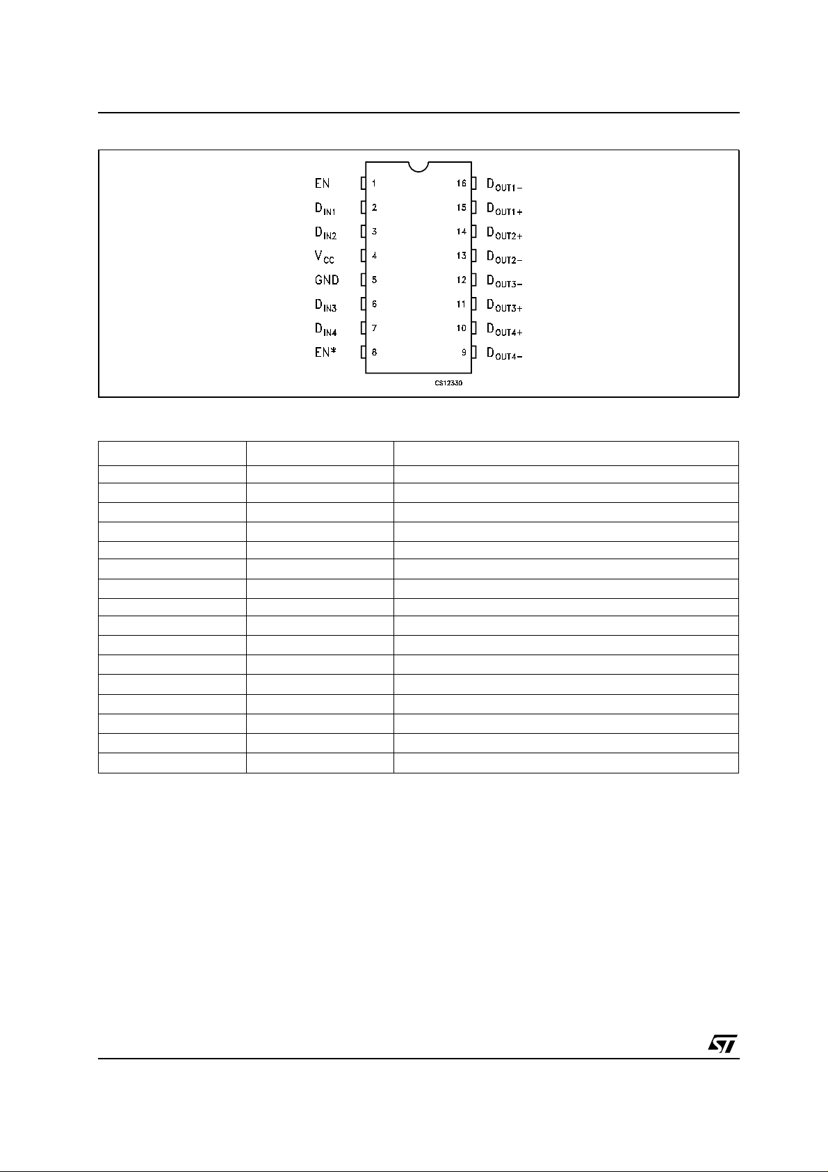
PIN CONFIGURATION
PIN DESCRIPTION
PlN N° SYMBOL NAME AND FUNCTION
1 EN Enable
2
3
4
5 GND GROUND
6
7
8 EN* Enable (inverting)
9D
10
11
12
13
14
15
16
D
D
V
D
D
OUT4-
D
OUT4+
D
OUT3+
D
OUT3-
D
OUT2-
D
OUT2+
D
OUT1+
D
OUT1-
IN1
IN2
CC
IN3
IN4
First Driver Input
Second Driver Input
Supply Voltage
Third Driver Input
Fourth Driver Input
Fourth Driver Inverting Output
Fourth Driver non-Inverting Output
Third Driver non-Inverting Output
Third Driver Inverting Output
Second Driver Inverting Output
Second Driver non-Inverting Output
First Driver non-Inverting Output
First Driver Inverting Output
2/10
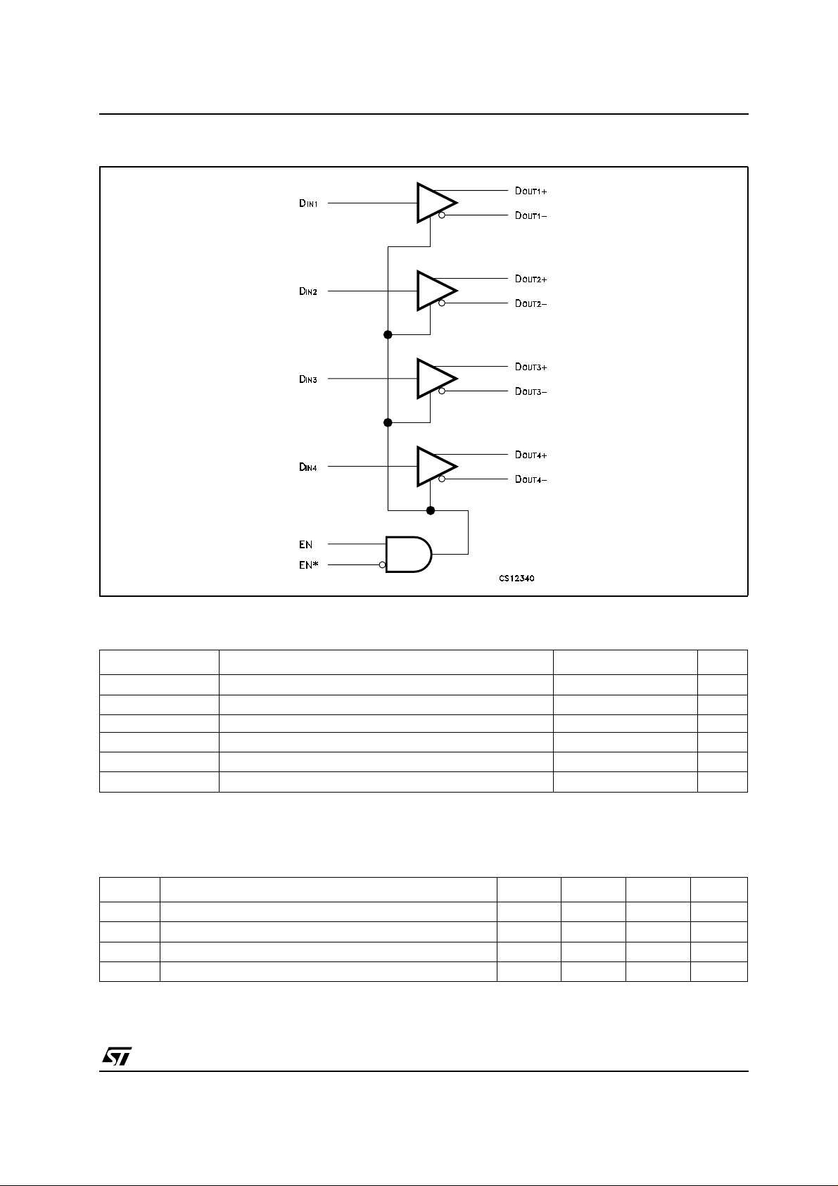
FUNCTIONAL DIAGRAM
STLVDS47
ABSOLUTE MAXIMUM RATINGS
Symbol Parameter Value Unit
V
CC
D
IN
Supply Voltage
Input Voltage
-0.3 to 4 V
-0.3 to 6 V
EN, EN* Enable Input Voltage -0.3 to 6 V
D
OUT+,DOUT-
I
SCTOUT
T
stg
Absolute Maximum Ratings are those values beyond which damage to the device may occur. Functional operation under these condition is
not implied.
Output Voltage
Short Circuit Duration
Storage Temperature Range
-0.3 to 3.9 V
Continuous
-65 to +150 °C
RECOMMENDED OPERATIN G CONDITIONS
Symbol Parameter Min TYP Max Unit
V
V
V
Supply Voltage
CC
High-Level Input Voltage
IH
Low-Level Input Voltage
IL
Operating Free-Air Temperature
T
A
3 3.3 3.6 V
2V
0.8 V
-40 85 °C
3/10
 Loading...