

SGS Thomson Microelectronics STLVDS3487BDR, STLVDS3487BTR, STLVDS3487BD, STLVDS31BDR, STLVDS31BTR Datasheet
...
1/13May 2003
■ MEETS OR EXCEEDS THE
REQUIREMENTS OF ANSI TIA/EIA-644
STANDARD
■ LOW VOLTAGE DIFFERENTIAL SIGNALING
WITH TYPICAL OUTPUT VOLTAGE OF
350mV AND A 100Ω LOAD
■ TYPICAL OUTPUT VOLTAGE RISE AND
FALL TIMES OF 750ps (400Mbps)
■ TYPICAL PROPAGATION DELAY TIMES OF
1.7ns
■ OPERATES FROM A SINGLE 3.3V SUPPLY
■ POWER DISSIPATION 25mW TYPICAL PER
DRIVER AT 200MHz
■ DRIVER AT HIGH IMPEDANCE WHEN
DISABLEDORWITHV
CC
=0V
■ PIN COMPATIBLE WITH THE AM26LS31,
SN65LVD31
■ LOW VOLTAGE TTL (LVTTL) LOGIC INPUT
LEVELS
DESCRIPTION
The STLVDS31 is a quad differential line drivers
that implements the electrical characteristics of
low voltage differential signaling (LVDS). This
signaling technique lowers the output voltage
levels of 5V differential standard levels (such as
TIA/EIA-422B) to reduce the power, increase the
switching speeds and allows operations with a
3.3V supply rail. Any of the four current mode
drivers will deliver a minimum differential output
voltage magnitude of 247m V into a 100Ω load
when enabled.
The intended application of this device and
signalling technique is for point-to-point baseband
data transmission over controlled impedance
media approximat ely 100Ω. The transmission
media may be printed circuit board traces,
backplanes or cables. The ultimate rate and
distance of data transfer is dependent upon the
attenuation characte ristics of the media and noise
coupling to the environment.
The STLVDS31 is characterized for op eration
from -40°C to 85°C.
ORDERING CODES
Type
Temperature
Range
Package Comments
STLVDS31BD -40 to 85 °C SO-16 (Tube) 50parts per tube / 20tube per box
STLVDS31BDR -40 to 85 °C SO-16 (Tape & Reel) 2500 parts per reel
STLVDS31BTR -40 to 85 °C TSSOP16 (Tape & Reel) 2500 parts per reel
STLVDS31
HIGH SPEED
DIFFERENTIAL LINE DRIVERS
SOP TSSOP
STLVDS31
2/13
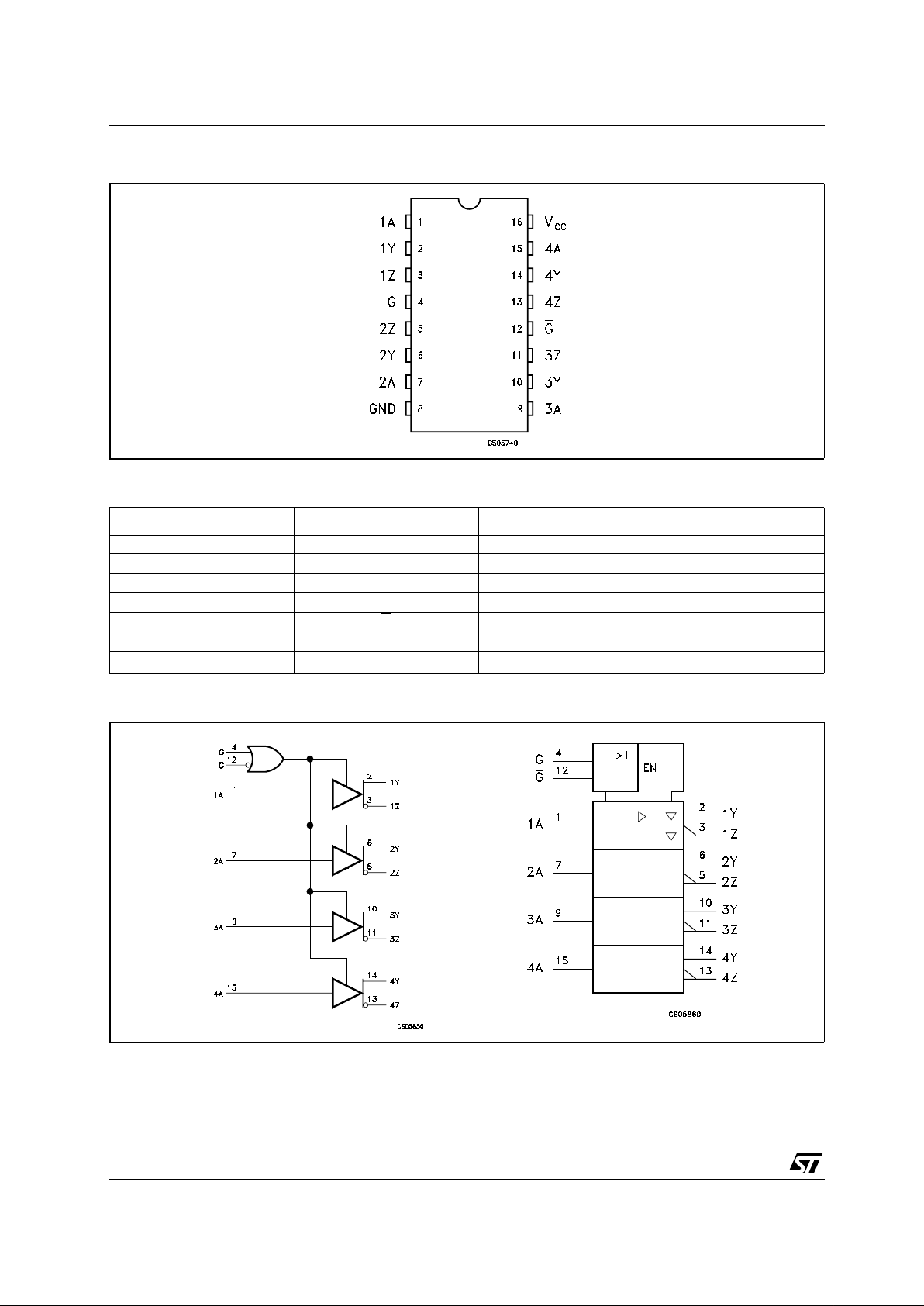
PIN CONFIGURATION
PIN DESCRIPTION
LOGIC DIAGRAM AND LOGIC SYMBOL
PlN N° SYMBOL NAME AND FUNCTION
1, 7, 9, 15 1A to 4A Driver Inputs
2, 6, 10, 14 1Y to 4Y Driver Outputs
3, 5, 11, 13 1Z to 4Z Driver Outputs
4 G Enable
12 G
Enable
8 GND Ground
16
V
CC
Supply Voltage
STLVDS31
3/13
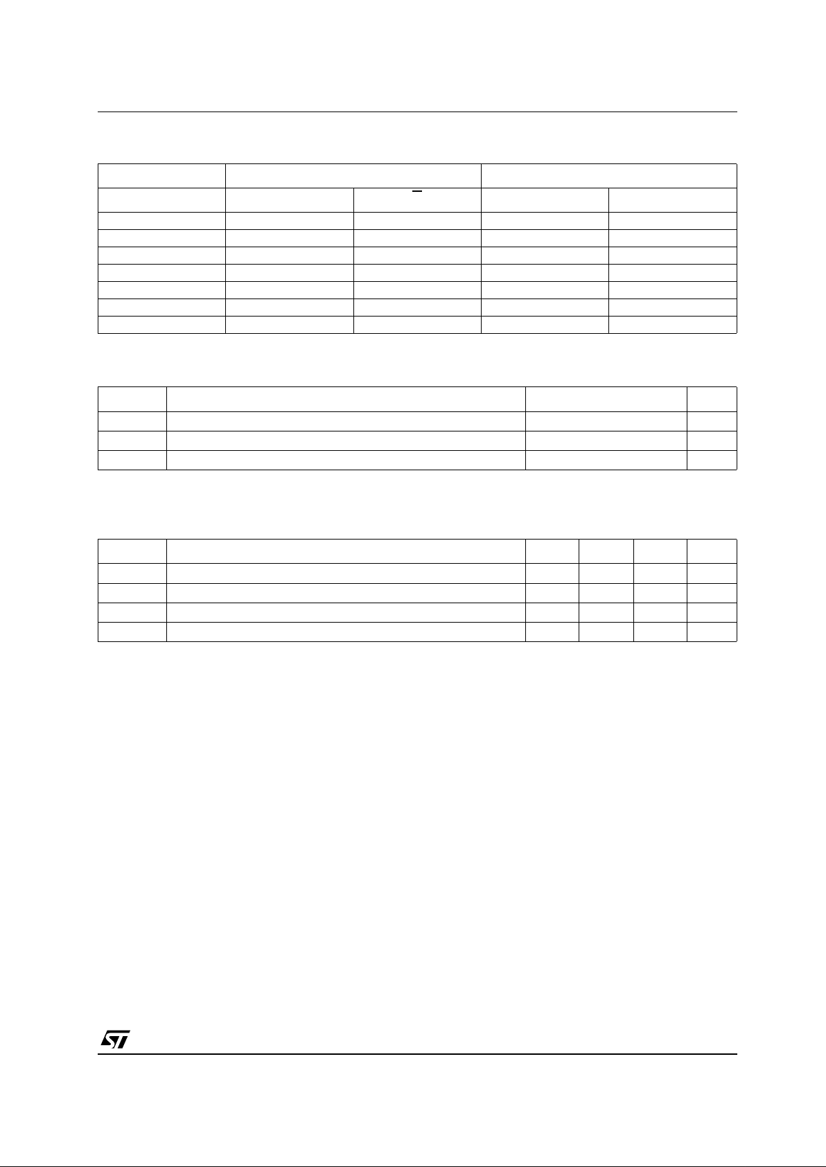
TRUTH TABLE
L=Low level, H=High Level, X=Don’t care, Z= High Impedance
ABSOLUTE MAXIMUM RATINGS
Absolute Maximum Ratings are those values beyond which damage to the device may occur. Functional operation under these condition is
not implied.
Note 1: All voltages except differential I/O bus voltage, are with respect to the network ground terminal.
RECOMMENDED OPERATING CONDITIONS
INPUT ENABLES OUTPUTS
AGG
YZ
HHXHL
LHXLH
HXLHL
LXLLH
XLHZZ
OPEN H X L H
OPEN X L L H
Symbol Parameter Value Unit
V
CC
Supply Voltage (Note 1)
-0.5 to 4.6 V
V
I
DC Input Voltage -0.5 to (VCC+ 0.5)
V
T
stg
Storage Temperature Range
-65 to +150 °C
Symbol Parameter Min. Typ. Max. Unit
V
CC
Supply Voltage 3.0 3.3 3.6 V
V
IH
HIGH Level Input Voltage 2.0 V
V
ILI
LOW Level Input Voltage 0.8 V
T
A
Operating Temperature Range
-40
85
°C
STLVDS31
4/13
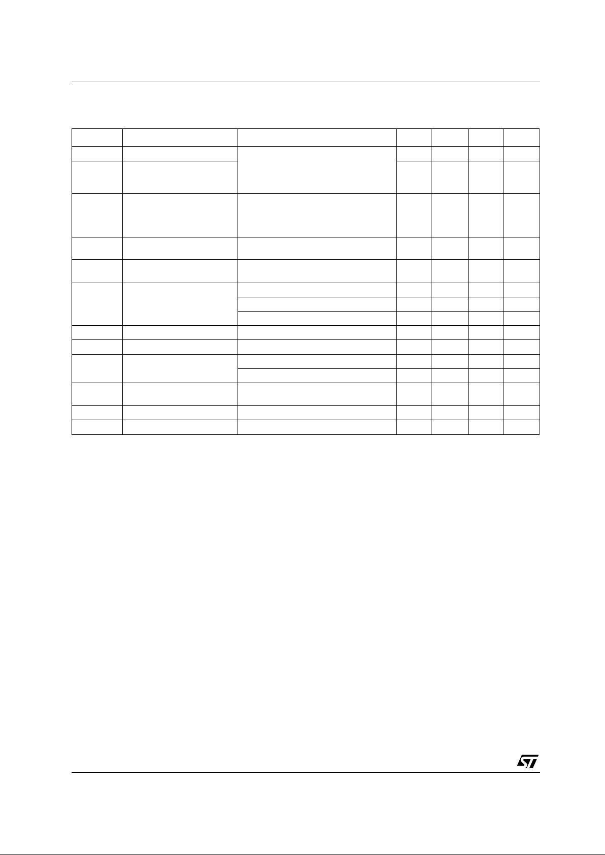
ELECTRICAL CHARACTERISTICS (Over recommended operating conditions unless otherwise noted.
All typical values are at T
A
= 25°C, and VCC=3.3V)
Symbol Parameter Test Conditions Min. Typ. Max. Unit
V
OD
Differential Output Voltage RL= 100Ω Fig. 2 247 350 454 mV
∆V
OD
Change in Differential
Output Voltage Between
Logic State
-50 50 mV
∆V
OC(SS)
Change in Steady-state
Common Mode Output
Voltage Between Logic
State
Fig. 3 1.125 1.2 1.375 V
V
OC(SS)
Steady-state Common
Mode Output Voltage
Fig. 3 -50 50 mV
V
OC(PP)
Peak to Peak Common
mode Output Voltage
80 150 mV
I
CC
Supply Current VIN= 0.8V or 2V, Enabled, No Load 11.5 20 mA
V
IN
= 0.8V or 2V, Enabled, RL=100Ω 25 35 mA
V
IN
= 0 or VCC, Disabled 0.3 1 mA
I
IH
High Level Input Current VIH=2V 4 20 µA
I
IL
Low Level Input Current VIL= 0.8V 0.6 10 µA
I
SC
Short Circuit Output Current V
O(Y)
or V
O(Z)
= 0V 6.1 -24 mA
V
OD
=0 ± 12 mA
I
OZ
High Impedance Output
Current
VO= 0 or 2.4V ± 1 µA
I
OFF
Power OFF Output Current VCC=0 VO= 2.4V ± 1 µA
C
IN
Input Capacitance 3 pF
 Loading...