

SGS Thomson Microelectronics STLVDS050BTR, STLVDS050BDR, STLVDS050BD Datasheet
HIGH SPEED DIFFERENTIAL LINE
■ MEETS OR EXCEED THE REQUIREMENTS
OF ANSI EIA/TIA-644-1995 STANDARD
■ SIGNALING RATESUP TO 400Mbit/s
■ BUS TERMINAL ESD EXCEEDS 6KV
■ OPERATES FROM A SINGLE 3.3V SUPPLY
■ LOW-VOLTAGE DIFFERENTIAL SIGNALING
WITH TYPICAL OUTPUT VOLTAGE OF
350mV AND A 100Ω LOAD
■ PROPAGATIONDELAY TIMES:
DRIVER: 2ns (TYP)
RECEIVER: 3ns (TYP)
■ POWER DISSIPATION AT 200MHz:
DRIVER: 25mW (TYP)
RECEIVER: 60mW (TYP)
■ LVTTL INPUT LEVELS ARE 5V TOLERANT
■ RECEIVER HAS OPEN-CIRUIT FAIL-SAFE
DESCRIPTION
The STLVDS050 is differential line drivers and
receivers that use low-voltage differential
signaling (LVDS) to achieve signal ing rate as high
as 400Mbps.
The EIA/TIA-644 standard compliant electrical
interface provides a minimum differential output
voltage magnitude of 247 mV into a 100 Ω load
and receipt of 100 mV signals with up to 1 V of
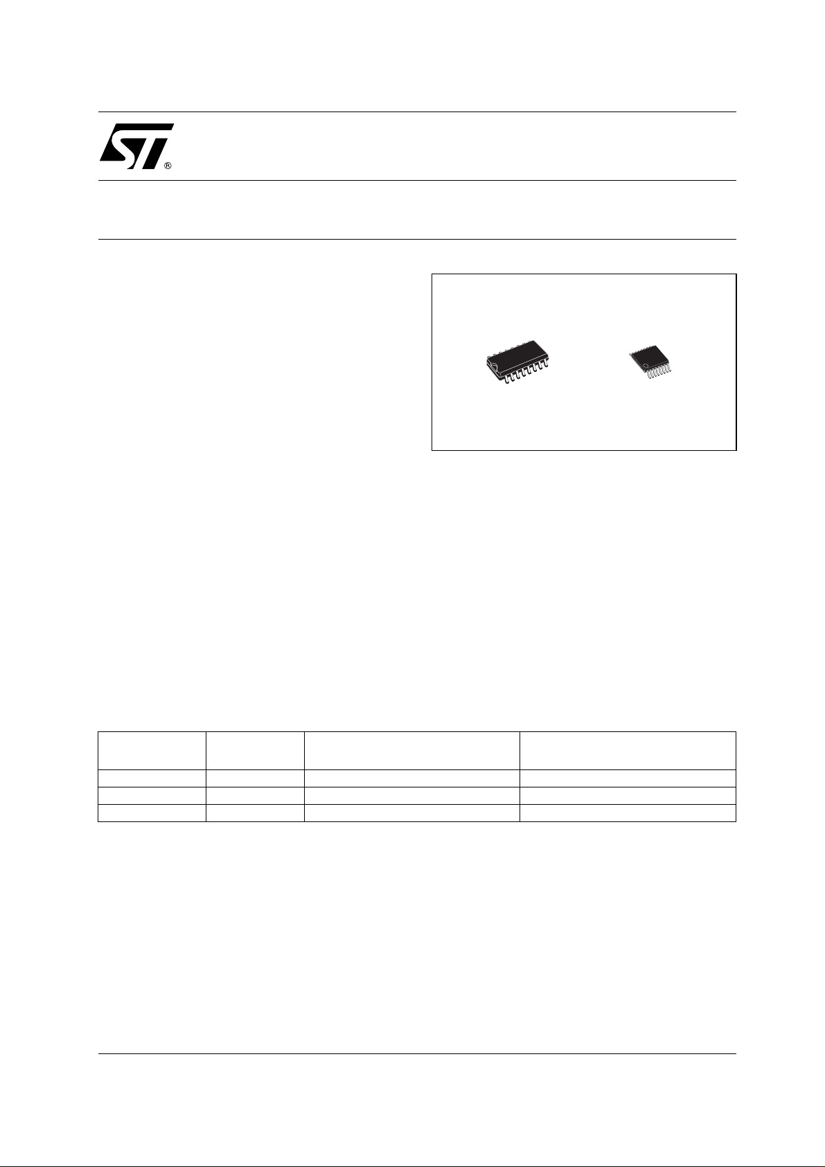
STLVDS050
DRIVERS AND R ECEIVERS
SOP TSSOP
ground potential difference between a t rans mi tter
and receiver.
The intended application of this device an
signaling technique is for point-to-point baseband
data transmission over controlled impedance
media of approximately 100 Ω characteristic
impedance.
The transmission media may be printed-circuit
board traces, backplanes, or cables. (Note: T he
ultimate rate and distance of data transfer is
dependent upon the attenuation characteristics of
the media, the noise coupling to the environme nt,
and other appl ication specific characteristics).
ORDERING CODES
Type
STLVDS050BD -40 to 85 °C SO-16 (Tube) 50 parts per tube / 20 tube per box
STLVDS050BDR -40 to 85 °C SO-16 (Tape & Reel) 2500 parts per reel
STLVDS050BTR -40 to 85 °C TSSOP16 (Tape & Reel) 2500 parts per reel
Temperature
Range
Package Comments
1/11May 2003
STLVDS050
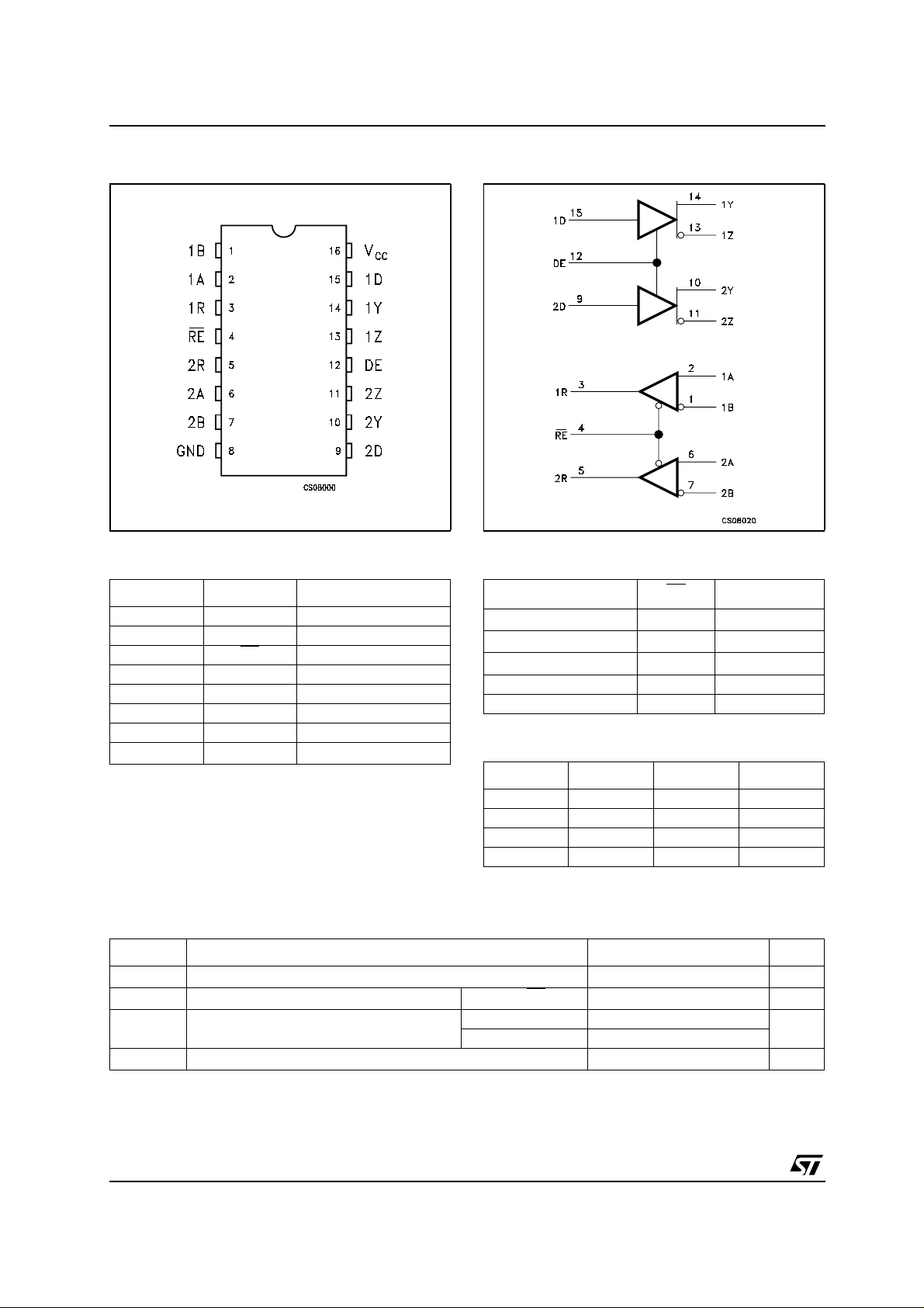
PIN CONFIGUR ATION
PIN DESCRIPTION
PlN N° SYMBOL NAME AND FUNCTION
1,2,6,7
3, 5 1R, 2R Receiver Outputs
4RE
9, 15 2D, 1D Driver Inputs
12 DE Driver Enable
10, 11, 13, 14 2Y, 2Z, 1Y, 1Z Driver Outputs
8 GND Ground
16
1A, 1B, 2A, 2B
V
CC
Receiver Inputs
Receiver Enable
Supply Voltage
FUNCTIONAL DIAGRAM
TRUTH TABLE FOR RECEIVER
VID=VA-V
V
≥ 100mV
ID
-100mV < V
≤ −100mV
V
ID
OPEN L H
B
< 100mV
ID
XHZ
RE R
LH
L?
LL
TRUTH TABLE FOR DRIVER
DDEY Z
LHLH
HHHL
OPEN H L H
XLZZ
L=Low level, H=High Level, X=Don’t care, Z= High Impedance
ABSOLUTE MAXIMUM RATINGS
Symbol Parameter Value Unit
V
V
ESD ESD Protection Voltage (HBM) Y, Z, A, B, and GND ± 6
T
Absolute Maximum Ratings are those values beyond which damage to the device may occur. Functional operation under these condition is
not implied.
2/11
Supply Voltage
CC
Voltage Range D, R, DE, RE
I
Storage Temperature Range
stg
-0.5 to 4 V
-0.5 to 6 V
All Pins ± 3
-65 to +150 °C
KV

STLVDS050
RECOMMENDED OPERATING CONDITIONS
Symbol Parameter Min. Typ. Max. Unit
V
V
V
|V
V
T
Supply Voltage 3.0 3.3 3.6 V
CC
HIGH Level Input Voltage 2.0 V
IH
LOW Level Input Voltage 0.8 V
IL
| Magnitude Of Differential Input Voltage 0.1 0.6 V
ID
Common Mode Input Voltage |VID|/2 24-|VID|/2 V
IC
-0.8
V
CC
Operating Temperature Range
A
-40
85
°C
ELECTRICAL CHARACTERISTICS (Typical values are at T
= 25°C, VCC= 3.3V ±10%, TA= -40 to 85°C
A
unless otherwise specified)
Symbol Parameter Test Conditions Min. Typ. Max. Unit
I
CC
Supply Current Drivers and Receivers enabled, No
receiver loads, Driver R
=100Ω
L
Driver enabled, Receivers disabled,
=100Ω
R
L
Drivers Disabled, Receiver enabled,
No load
Disabled 0.5 1
DRIVER ELECTRICAL CHARACTERISTICS (Typical values are at T
T
= -40 to 85°C unless otherwise specified)
A
= 25°C, VCC=3.3V±10%,
A
Symbol Parameter Test Conditions Min. Typ. Max. Unit
| Differential Output Voltage
|V
OD
Magnitude
∆|V
| Change in Differential
OD
Output Voltage Magnitude
RL= 100Ω 247 340 454 mV
= 100Ω -50 50 mV
R
L
Between Logic States
∆V
OC(SS)
Change in Steady-state
Common Mode Output
-50 50 mV
Voltage Between Logic
States
V
OC(SS)
V
OC(PP)
Steady-state Common
Mode Output Voltage
Peak to Peak Common
mode Output Voltage
I
High Level Input Current VIH= 5V DE -0.5 -20 µA
IH
1.125 1.2 1.375 V
D220µA
I
Low Level Input Current VIL= 0.8V DE -0.5 -10 µA
IL
D110µA
I
OS
I
OZ
I
O(OFF)
C
Short Circuit Output Current V
High Impedance Output
Current
or V
O(Y)
=0 4 10 mA
V
OD
=0V 6 10 mA
O(Z)
VO= 600mV ± 1 µA
=0VorV
V
O
CC
Power OFF Output Current VCC=0V VO= 3.6V ± 1 µA
Input Capacitance 3 pF
IN
12 20 mA
10 16
46
50 150 mV
± 1 µA
3/11

STLVDS050
RECEIVER ELECTRICAL CHARACTERISTICS (Typical values are at TA=25°C,VCC= 3.3V ±10%,
T
= -40 to 85°C unless otherwise specified)
A
Symbol Parameter Test Conditions Min. Typ. Max. Unit
V
ITH+
V
ITH-
V
V
I
I(OFF)
I
I
I
OZ
C
Positive-going Differential
Input Voltage Threshold
Negative-going Differential
-100 mV
Input Voltage Threshold
High Level Output Voltage IOH= -8mA 2.4 V
OH
Low Level Output Voltage IOL= 2mA 0.4 V
OL
Input Current (A or B Inputs) VI=0V -2 -11 -20 µA
I
I
= 2.4V -1 -3 µA
V
I
Power OFF Input Current
VCC=0V ±20 µA
(A or B Inputs)
High Level Input Current
IH
(Enable)
Low Level Input Current
IL
(Enable)
High Impedance Output
VIH=5V ±10 µA
VIL= 0.8V ±10 µA
VO= 0 or 5V ± 10 µA
Current
Input Capacitance 3 pF
IN
100 mV
DRIVER SWITCHING CHARACTERISTICS (Typical values are at T
T
= -40 to 85°C unless otherwise specified)
A
= 25°C, VCC=3.3V±10%,
A
Symbol Parameter Test Conditions Min. Typ. Max. Unit
t
PLH
t
PHL
t
sk(P)
Propagation Delay Time,
Low to High Output
Propagation Delay Time,
High to Low Output
Differential Output Signal
t
r
Rise Time
Differential Output Signal
t
f
Fall Time
Pulse Skew (|t
THL-tTLH
RL= 100Ω CL= 10pF 2 2.7 ns
2 2.7 ns
0.4 1 ns
0.4 1 ns
|)
50 ps
(note1)
t
sk(O)
t
PZH
Channel-to-channel Output
Skew (note2)
Propagation Delay Time,
High Impedance to High
40 ps
610ns
Level Output
Propagation Delay Time,
t
PZL
High Impedance to Low
610ns
Level Output
Propagation Delay Time,
t
PHZ
High Level to High
310ns
Impedance Output
Propagation Delay Time,
t
PLZ
Low Level to High
310ns
Impedance Output
4/11
 Loading...