

SGS Thomson Microelectronics STLVD210BFTR, STLVD2101BF Datasheet
1/9December 2002
■ 100ps PART-TO-PART SKEW
■ 50ps BANK SKEW
■ DIFFERENTIAL DESIGN
■ MEETS LVDS SPEC. FOR DRIVER
OUTPUTS AND RECEIVER INPUTS
■ REFERENCE VOLTAGE AVAILABLE
OUTPUT V
BB
■ LOW VOLTAGEV
CC
RANGE OF 2.375V TO
2.625V
■ HIGH SIGNALLING RATE CAPABILITY
(EXCEEDS 700MHz)
■ SUPPORT OPEN, SHORT, AND
TERMINATED INPUT FAIL-SAFE (LOW
OUTPUT STATE)
■ PROGRAMMABLE DRIVERS POWER OFF
CONTROL
DESCRIPTION
The STLVD210 is a low skew programmable
1-to-5 dual differential LV DS drive r, designed with
clock distribution in mind. The LVDS input signals
can be either differential or single-ended if the
VBB output is used.
The STLV D210 is provided with a 11 bit shift
register with a serial in and a Control Register.
The purpose is to enable or power off each output
clock channel and to select the clock input . The
STLVD210 is s pec ific ally designed, modelled and
produced with low s ke w as the key goal. Optimal
design and layout serve to minimize gate to gate
skew within a device. The net result is a
dependable guaranteed low skew dev ice.
The STLVD210 can be used for high performanc e
clock distribution in 2.5V systems wi th LVDS
levels. Designers can be take advantage of the
device’s performance to d istribute low skew
clocks across the backplane or the board.
ORDERING CODES
Type
Temperature
Range
Package Comments
STLVD210BF -40 to 85 °C TQFP32 (Tray) 250 parts per Tray
STLVD210BFR -40 to 85 °C TQFP32 (Tape & Reel) 2400 parts per reel
STLVD210
DIFFERENTIAL LVDS CLOCK DRIVER
TQFP32
STLVD210
2/9
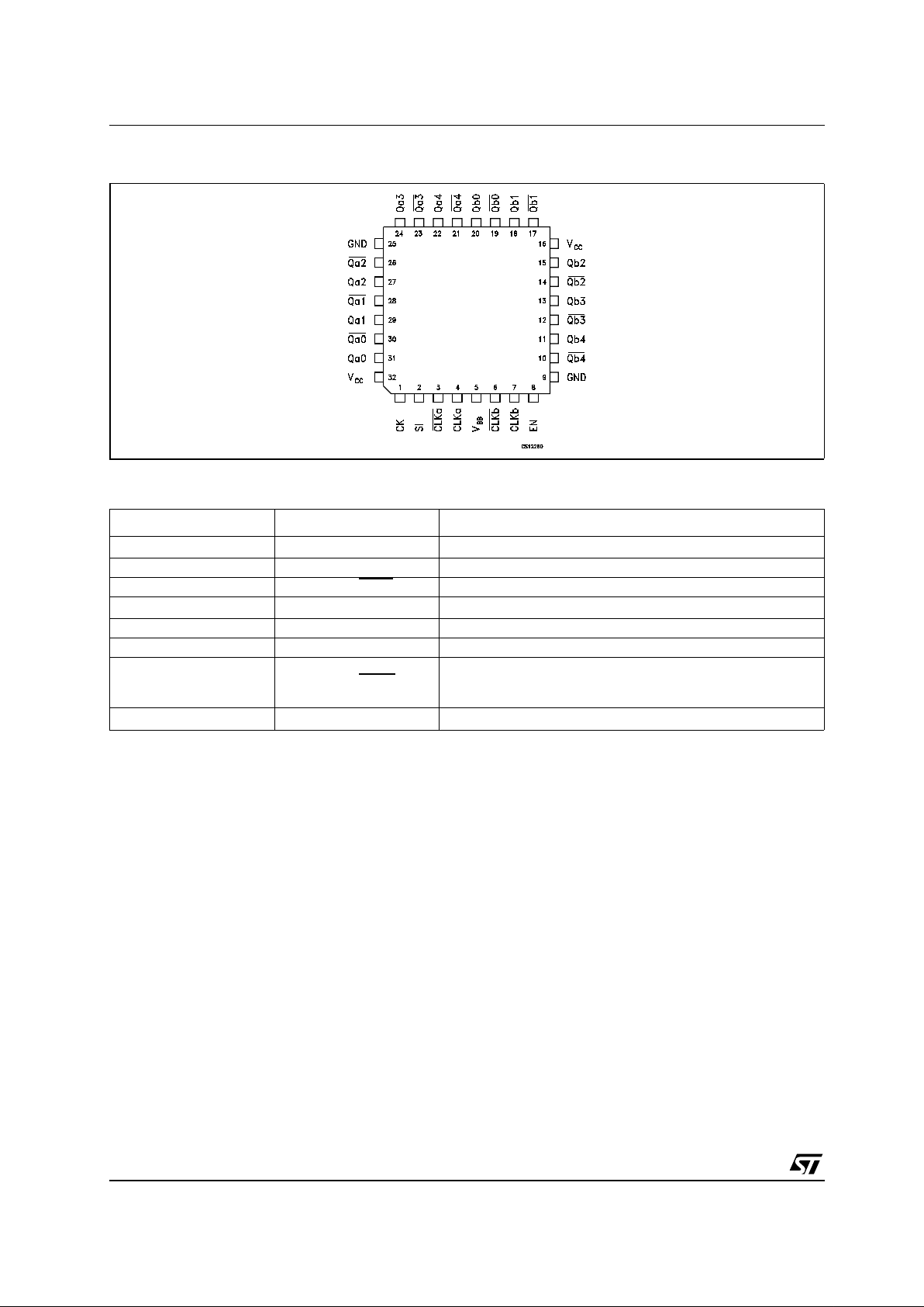
PIN CONFIGURATION
PIN DESCRIPTION
PlN N° SYMBOL NAME AND FUNCTION
1 CK Control Register Clock
2 SI Control Register Serial IN/CLK_SEL
3, 4, 6, 7 CLKn/CLKn
LVDS CLK Inputs
5
V
BB
Reference Voltage Output
8 EN Device Enable/Program
9, 25 GND GROUND
10, 11, 12, 13, 14, 15, 17,
18, 19, 20, 21, 22, 23, 24,
26, 27, 28, 29, 30, 31
Qn0:4/Qn0:4
LVDS
16, 32
V
CC
Supply Voltage
STLVD210
3/9
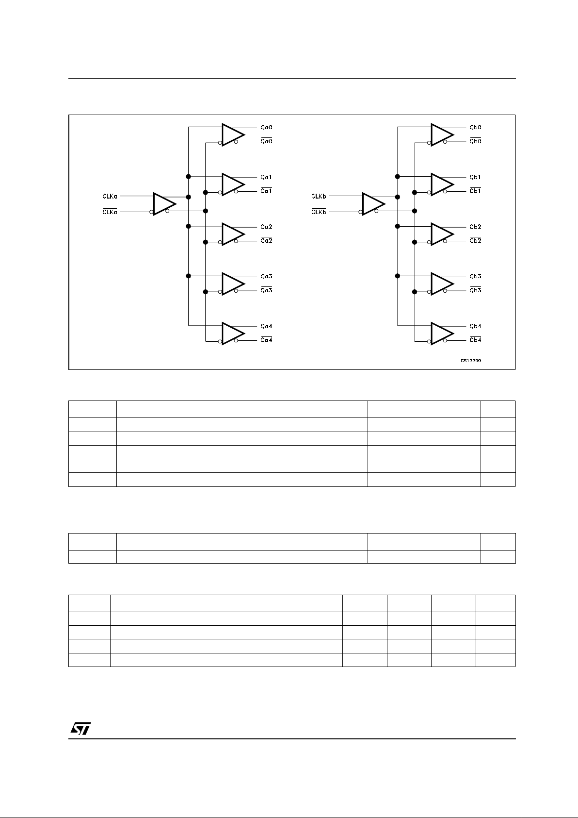
LOGIC DIAGRAM
ABSOLUTE MAXIMUM RATINGS
Absolute Maximum Ratings are those values beyond which damage to the device may occur. Functional operation under these condition is
not implied.
THERMAL DATA
RECOMMENDED OPERATIN G CONDITIONS
Symbol Parameter Value Unit
V
CC
Supply Voltage
-0.3 to 2.8 V
V
I
Input Voltage -0.2 to (VCC+0.2)
V
V
O
Output Voltage -0.2 to (VCC+0.2)
V
I
OSD
Driver Short Circuit Current
Continuous
ESD Electrostatic Discharge (HBM 1.5KΩ, 100pF)
>2 KV
Symbol Parameter Value Unit
R
Tj-c
Thermal Resistance Junction-Case
13 °C/W
Symbol Parameter Min TYP Max Unit
V
CC
Supply Voltage
2.375 2.625 V
V
IC
Receiver Common Mode Input Voltage 0.5(VID) 2-0.5(VID)
V
T
OPR
Operating Free-Air Temperature Range
-40 85 °C
T
J
Operating Junction Temperature
-40 105 °C
 Loading...