


SGS Thomson Microelectronics STLC7550 Datasheet

STLC7550
LOW POWE R LO W VO LTAGE ANALOG FRONT E ND
.
GENERAL PURPOSE SIGNAL PROCESSING
ANALOG FRONT END (AFE)
.
TARGETED FOR V.34bis MODEM AND
56Kbps MODEM APPLICATIONS
.
16-BIT OVERSAMPLING Σ∆ A/D AND D/A
CONVERTERS
.
83dB SIGNAL TO NOISE RATIO FOR SAMPLING FREQUENCY UP TO 9.6kHz @ 3V
.
87dB DYNAMIC RANGE @ 3V
.
FILT ER BAND W IDTHS :
0.425 x THE SAMPLING FREQUENCY
.
ON-CHIP REFERENCE VOLTAGE
.
SINGLE POWER SUPPLY RANGE :
2.7 TO 5.5V
.
LOW POWER CONSUMPTION LESS THAN
30mW OPERATING POWER 3V
.
STAND-BY MODE POWER CONSUMPTION
LESS T HAN 3µW at 3V
.
PROGR AM MI N G SA MPLING FREQ U E N CY
.
MAX. SAMPLING FREQUENCY : 45kHz
.
SYNCHRONOUS SERIAL INTERFACE FOR
PROCESSO R DATAS EXCHANGE. MAS TER
OR SLAVE OPERA TIONS
.
0.50µm CMOS PROCESS
.
TQFP44 PACKAGE
.
STLC7546 MODE OF OPERATION COMP A TIBLE
Maximum Power Dissipation 30mW is well suited
for Battery operations.
In case of battery low, STLC7550 will continue to
work even at a 2.7V level.
STLC7550 also provides clock generator for all
sampling frequencies requested for V.34bis and
56Kbps applications.
This new AFE can also be used for PC mother
boards or add-on cards or stand alone MODEMs.
It can be used in a master mode or slave mode.
The slave mode eases multi AFE architecture design in saving external logical glue.
TQFP44 (10 x 10 x 1.40 mm)
(Full Plastic Quad Flat Pack)
ORDER CODE : STLC7550TQFP
DESCRIPTION
The STLC7550 is a single chip Analog Front-end
(AFE) designed to implement modems up to
56Kbps.
It has been espec ially des igned fo r hos t proc ess ing
application in which the modulation software
(V .34bi s, 56Kbps) is perf ormed by the main app lication proces s or : Pentium, Risc or D S P pr oc es s or s .
The main target of this device is stand alone appliances as Hand Held PC (HPC), Personnal Digital
Assistants (PDA), Webphones, Network Computers, Set Top Boxes for Digital Television (Satellite
and Cable).
To comply with such applications STLC7550 is
powered nominally at 3V only.
November 1998
TQFP48 (7 x 7 x 1.40mm)
(Full Plastic Quad Flat Pack)
ORDER CODE : STLC7550TQF7
1/17
STLC7550
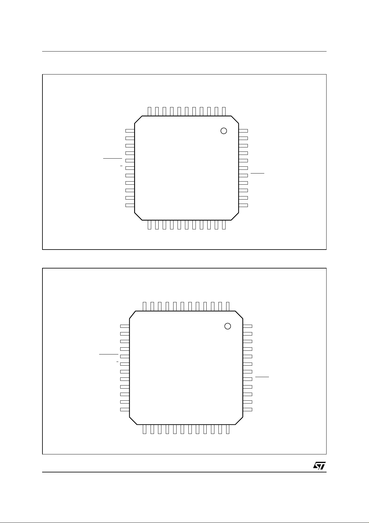
PIN CONNECTIONS
(TQFP44)
HC1
HC0
PWRDWN
M/S
V
REFP
V
REFN
AGND1
XTALIN/MCLK
XTALOUT
MCM
DGND
DVDDFS
12
13
14
15
16
17
18
19
20
21
22
23 24 25 26 27 28 29 30 31 32 33
DD
IN-
IN+
AUXIN-
AUXIN+
AV
CM
V
SCLK
AGND2
1234567891011
44
43
42
41
40
39
38
37
36
DOUT
DIN
TSTD1
TS
RESET
OUT-
OUT+
35
34
7550-01.EPS
PIN CONNECTIONS
(TQFP48)
HC1
HC0
PWRDWN
M/S
V
REFP
V
REFN
AGND1
MCM
DGND
DD
DV
XTALOUT
13
14
15
16
17
18
19
20
21
22
23
24
25 26 27 28 29 30 31 32 331234 35 36
DD
CM
IN-
AV
V
IN+
AUXIN- XTALIN/MCLK
AUXIN+
FS
SCLK
AGND2
1234567891011
48
47
46
45
44
43
42
41
40
39
DOUT
DIN
TSTD1
TS
RESET
OUT-
OUT+
38
37
7550-01.EPS
2/17
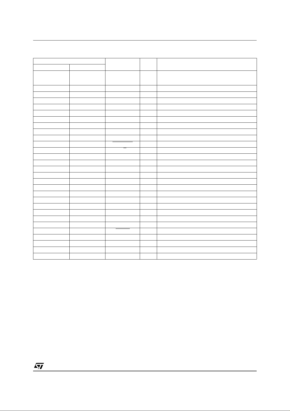
PIN LIST
Pin Number
TQFP44 TQFP48
1 - 2, 10 to 13,
21 to 24, 32 to
35, 43 - 44
3 3 SCLK O Shift Clock Output
4 4 FS I/O Frame Synchronization Input (slave)/Output (master)
55DV
6 6 DGND I Digital Ground
7 7 MCM I Master Clock Mode
8 8 XTALOUT O Crystal Output
9 9 XTALIN/MCLK I Crystal Input (MCM = 1) / External Clock (MCM = 0)
14 15 HC1 I Hardware Control Input
15 16 HC0 I Hardware Control Input
16 17
17 18 M/
18 19 V
19 20 V
20 21 AGND1 I Analog Ground
25 27 AUXIN+ I Non-inverting Input to Auxiliary Analog Input
26 28 AUXIN- I Inverting Input to Auxiliary Analog Input
27 29 IN+ I Non-inverting Input to Analog Input Amplifier
28 30 IN- I Inverting Input to Analog Input Amplifier
29 31 AV
30 32 V
31 33 AGND2 I Analog Ground
36 39 OUT+ O Non-inverting Smoothing Filter Output
37 40 OUT- O Inverting Smoothing Filter Output
38 41
39 42 TS I Timeslot Control Input
40 43 TSTD1 I/O Digital Input/Output reserved for test
41 44 DIN I Serial Data Input
42 45 DOUT O Serial Data Output
1 - 2, 10 to 14,
22 to 26, 34 to
38, 46 to 48
STLC7550
Name Type Description
NC - Not connected
DD
PWRDWN I Power down Input
S I Master/Slave Mode Control Pin Input
REFP
REFN
DD
CM
RESET I Reset Function to initialize the internal counters
I Positive Digital Power Supply (2.7V TO 5.5V)
O 16-bit D/A and A/D Positive Reference Voltage
O 16-bit D/A and A/D Negative Reference Voltage
I Positive Analog Power Supply (2.7V to 5.5V)
O Common Mode Voltage Output (AVDD/2)
7550-01.TBL
PIN DESCRIPTION
Supply
DD
(5 pins)
(AV
DD
1.2 - Digital V
)
This pin is the positive digital power s upply for DAC
Supply
DD
and ADC digital internal circuitry.
1.3 - Analog Ground
supply
DD
These pins are the ground return of the analog DAC
(ADC) section.
1.4 - Digital Ground
This pin is the ground for DAC and ADC internal
digital circuitry.
and Digital VDD shoul d be d ecoup led wit h re sp ect to An alo g Gro u nd an d Dig ita l
DD
1 - POWER SUPPLY
1.1 - Analog V
This pin is the positive analog power supply
voltage for the DAC and the ADC sect ion.
It is not internally connected to digital V
(DV
).
DD
In any case the voltage on this pin must be higher
or equal to the voltage of the Digital power supply
).
(DV
DD
Notes :
1. To obtain published performance, the analog V
Ground, respecti vely. The decoupling is intended to isolate digital no i se from the ana l og sectio n ; dec oupling capaci tors sho uld
be as clo se as possi ble to the respective analog and dig i tal suppl y pins.
2. All the ground pins m ust b e tied toget her. In the following sec tion, the ground and s upply pins are referred t o as GND and V
respectively.
(DV
(AGND1, AGND2)
(DGND)
DD
)
DD
3/17
,

STLC7550
PIN DESCRIPTION
2 - HOST INTERFACE
2.1 - Data In
(DIN)
(continued)
(10 pins)
In Data Mode, the data word is the input of the DAC
channel. In software, the data word is followed by
the control register word.
2.2 - Data Out
(DOUT)
In Data Mode, the data word is the ADC conversion
result. In software, the data word is followed by t he
register read.
2.3 - Frame Synchronization
(FS)
In master mode, the frame synchronization signal
is used to indicate that the device is ready to send
and receive data. The data trans fer begins on the
falling edge of the frame-sync signal. The framesync is generated internally and goes low on the
rising edge of SCLK in master mode. In slave mode
the frame is generated externally.
2.4 - Serial Bit Clock
(SCLK)
SCLK clocks the digital data into DIN and out of
DOUT during the frame synchronization interval.
The Serial bit clock is generated internally .
RESET)
2.5 - Reset Function
(
The reset function is to initialize the internal counters and control register. A minimum low pulse of
100ns is required to reset the chip. This reset
function initiates the serial data communications.
The reset function will initialize all t he registers to
their default value and will put the device in a
pre-programmed state. After a low-going pulse on
RESET, the device registers will be initialized to
provide an over-sampling ratio equal to 160, the
serial interface will be in data mode, the DAC
attenuation will be set to infinite, the ADC gain will
be set to 0dB, the Differential i nput mode on the
ADC converter will be selected, and the multiplexor
will be set on the main inputs IN+ and IN-. After a
reset condition, the first frame synchronization corresponds to the primary channel.
(
2.6 - Power Down
PWRDWN)
The Power-Down input powers down the entire
chip (< 50µW). When
PWRDWN Pin is taken low,
the device powers down such that the existing
internally programmed state is maintained. When
PWRDWN is driven high, full operation resumes
after 1ms. If the
should be tied to V
2.7 - Hardware Control
PWRDWN input is not used, it
.
DD
(HC0, HC1)
These two pins are used for Hardware/Software
Control of the device. The data on HC0 and HC1
will be latched on to the device on the rising edge
of the Frame Synchronization Pulse. If these two
pins are low, Software Control Mode is selected.
When in Software Control Mode, the LSB of the
16-bit word will select the Data Mode (LSB = 0) or
the Control Mode (LSB = 1). Other combinations of
HC0/HC1 are for Hardware Control. These inputs
should be tied low if not used.
S)
2.8 - Master/Slave Control
When M/
S is high, the device is in master mode
and Fs is gen erate d internal ly. When M/
(M/
S is low,
the device is in slave mode and Fs must be
generat ed externall y.
2.9 - Master Clock Mode
(MCM)
When MCM is high, XTALIN is provide d external ly
and must be equal to 36.864MHz. When MCM is low,
XTALIN is provided externally and must be equal to
oversampling frequency : Fs x Over (see Clock Block
Diagram and §4 Modes of Operation).
2.10 - Timeslot Control
(TS)
When TS = 0 the data are assigned to the first
16 bits after falling edge of FS (7546 mode) otherwise the data are bits 17 to 32.
The case M/
S = 1 with TS = 1 is reserved for life-test
(transmit gain fixed to 0dB).
3 - CLOCK SIGNALS
(2 pins)
Depending on MCM value, these pins have different function.
3.1 - MCM = 1
(XTALIN, XTA LOUT)
These pins must be tied to external crystal. For the
value of crystal see Functional Description Chapter
Part 3.
3.2 - MCM = 0
(MCLK, XTALOUT)
MCLK Pin must be connected to an external c lock.
XT A LOUT is not used.
4/17
STLC7550
PIN DESCRIPTION
4 - ANALOG INTERFACE
(continued)
(9 pins)
4.1 - DAC and ADC Positive Reference
)
Voltage Output
(V
REFP
This pin provides the Positive Reference Voltage
used by the 16-bit conv erters. The reference voltage, V
V
REFP
1.25V. V
resp e ct to V
, is the voltage difference between the
REF
and V
REFP
outputs, and its nominal value is
REFN
should be externally decoupled with
.
CM
4.2 - DAC and ADC Negative Reference
Voltage Output
(V
REFN
)
This pin provides the Negative Reference Voltage
used by the 16-bit converters, and should be externally decoupled with respect to V
4.3 - Common Mode V oltage Output
CM
.
)
(V
CM
This output pin is the common mode voltage
(AV
- AGND)/2. This output must be decoupled
DD
with re s p e ct to GN D .
4.4 - Non- inverting Sm oothing Filter Outpu t
(OUT+)
This pin is the non-inverting output of the fully
differential analog smoothing filter.
4.5 - Inverting Smoothing Filter Output
(OUT-)
This pin is the inverting output of the fully differential
analog smoothing filter. Outputs OUT+ and OUTprovide analog signals with maximum peak-topeak amplitude 2 x V
, and must be followed by
REF
an external two pole smoothing filter. The external
filter follows the internal single pole switch capaci-
tor filter. The cutoff frequency of the external filter
must be greater than two times the sampling frequency (FS), so that the combined frequency response of both the internal and external filters is flat
in the passband . The attenuator of the last output
stage can be programmed to 0dB, 6dB or infinite.
4.6 - Non-inverting Analog Input (IN+)
This pin is the differential non-inverting ADC input .
4.7 - Inverting Analog Input
(IN-)
This pin is the differential inverting ADC input.
These analog inputs (IN+, IN-) are presented to the
Sigma-Delta modulator. The analog input peak-topeak differential signal range must be less than
2 x V
, and must be preceded by an external
REF
single pole anti-aliasing filter. The cut-off frequency
of the filter must be lower than one half the oversampling frequency. These filters should be set as
close as possible to the IN+ and IN- pins. The gain
of the first stage is programmable (see Table 3).
4.8 - Non-inverting Auxiliary Analog
Input
(AUX IN+)
This p in is th e dif ferentia l non-i nverti ng au xiliary ADC
input. The characteristics are same as the IN+ input.
4.9 - Inverting Auxiliary Analog Input
(AUX IN-)
This pin is the differential inverting auxiliary ADC
input. The characteristics are same as the IN- input.
The input pair (IN+/IN- or AUX IN+/AUX IN-) are
software selectable.
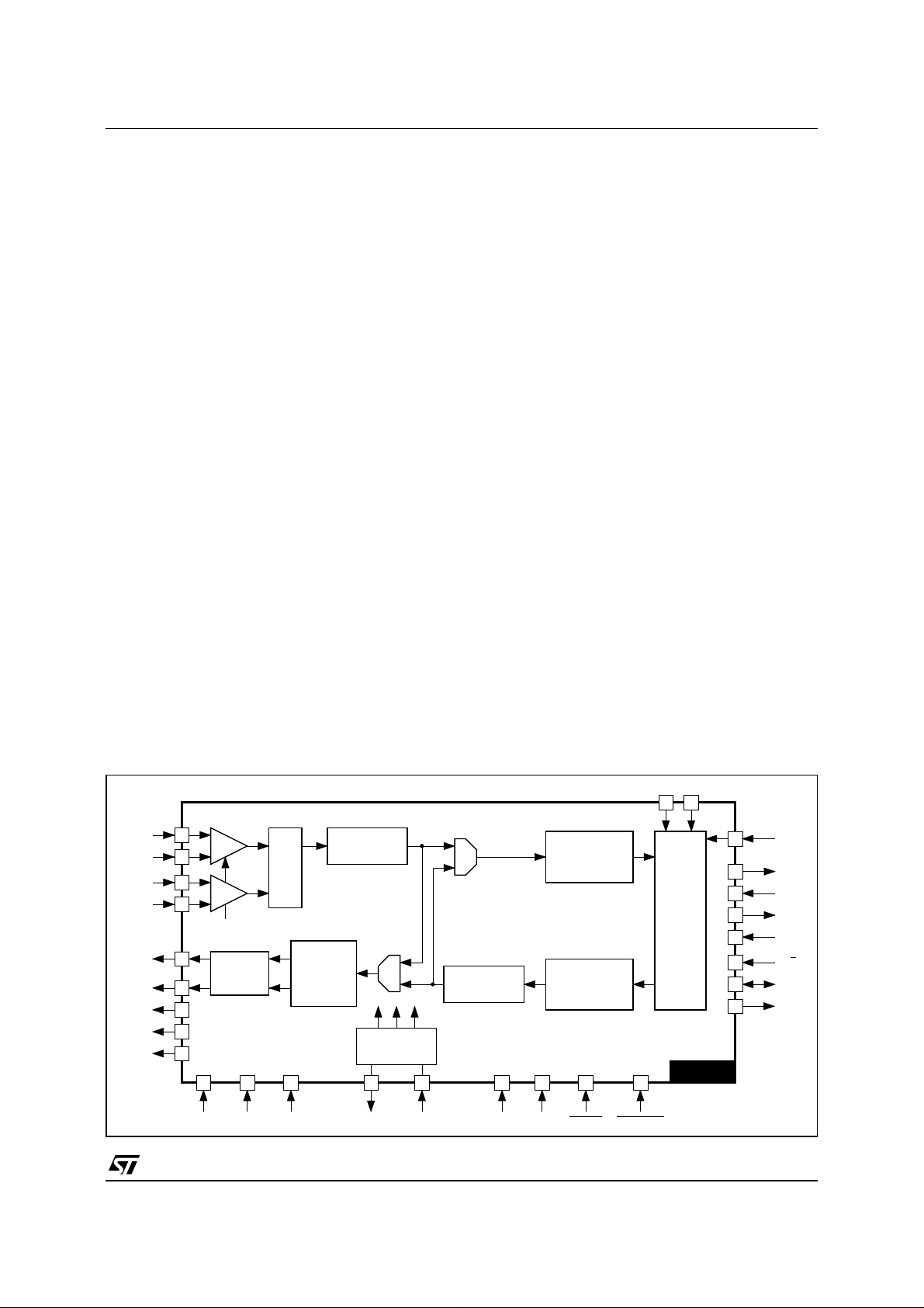
BLOCK DIAGRAM
27
IN+
28
IN-
REFP
REFN
V
25
26
(0 + 6dB in
diff. input)
36
37
18
19
30
CM
ATTEN.
0dB/+6dB/
INFINITE
DD
AUXIN+
AUXIN-
OUT+
OUT-
V
V
(TQFP44)
MUX
MODULATOR
DAC 1 BIT
First order
differential
switched
capacitor
filter
ANALOG
CLOCK
GENERATOR
HC1
HC0
15
14
7
LOW-PASS
(0.425 x sampling
frequency)
SERIAL PORTS
2nd ORDER
MODULATOR
XTALINXTALOUTAGND2AGND1AV
DVDDDGND
LOW-PASS
(0.425 x sampling
frequency)
38 166598312029
RESET PWRDWN
STLC7550
42
41
40
39
17
AND CONTROL REGISTER
MCM
DOUT
DIN
TSTD1
TS
M/S
4
FS
3
SCLK
7550-02.EPS
5/17
STLC7550
FUNCTIONAL DESCRIPTION
1 - TRANSMIT D/A SECTION
The functions included in the Tx D/A section are
detailed hereafter. 16-bit 2’s complement data format is used in the DAC channel.
1.1 - Transmit Low Pass Filters
The transmit low pass filter is basically an interpolating filter including a sinx/x correction. It is a
combination of Finite Impulse Res ponse filter (FIR)
and an Infinite Impulse Response filter (IIR). The
digital signal from the serial interface gets interpolated by 2, 3, 4, 5 or 6 x Sampling Frequency (FS)
through the IIR filter. The signal is further interpolated by 32 x FS x n (with n equal to 2, 3, 4, 5, 6)
through the IIR and FIR filter. The low pass filter is
followed by the DAC. The DAC is oversampled at
64, 96, 128, 160, 192 x FS. The oversampling ratio
is user selectable.
1.2 - D/A Converter
The oversampled D/A converter includes a second
order digital noise shaper, a one bit D/A converter
and a single pole analog low-pass filter.
The attenuation of the last output stage can be
programmed to 0dB, +6dB or infinite. The cut-off
frequency of the single pole switch-capacitor lowpass filter is :
fc
with OCLK = Oversampling Clock frequency.
Continuous-time filtering of the analog differential
output is necessary using an off-chip amplifier and
a few external passive components.
At least 79dB signal to noise plus distortion ratio can
be obtained in the frequency band of 0.425 x 9.6kHz
(with an oversampling ratio equal to 160).
2 - RECEIVE A/D SECTION
The different functions included in the ADC channel
section are described below . 16-bit 2’ s complement
data format is used in the ADC.
2.1 - A/D Converter
The oversampled A/D converter is based on a
second order sigma-delta modulator. To produce
excellent common-mode rejection of unwanted signals, the analog signal is processed differentially
until it is converted to digital data. Single-ended
mode can also be used. The ADC is oversampled
at 64, 96, 128, 160 or 192 x FS. The oversampling
ratio is user selectable. At least -85dB SNDR can
be expected in the 0.425 x 9.6kHz bandwidth with
a -6dBr differential input signal and an oversampling ratio equal to 160.
OCLK
=
−
3dB
2
⋅ π ⋅ 10
2.2 - Receive Low Pass Filter
It is a decimation filter . The decimation is performed
by two decimation digital filters : one decimation
FIR filter and one decimation IIR filter.
The purpose of the FIR filter is to decimate 32 times
the digital signal coming from the ADC modulator.
The IIR is a cascade of 5 biquads. It provides the
low-pass filtering needed to remove the noise remaining above half the sampling frequency. The
output of the IIR will be processed by the DSP .
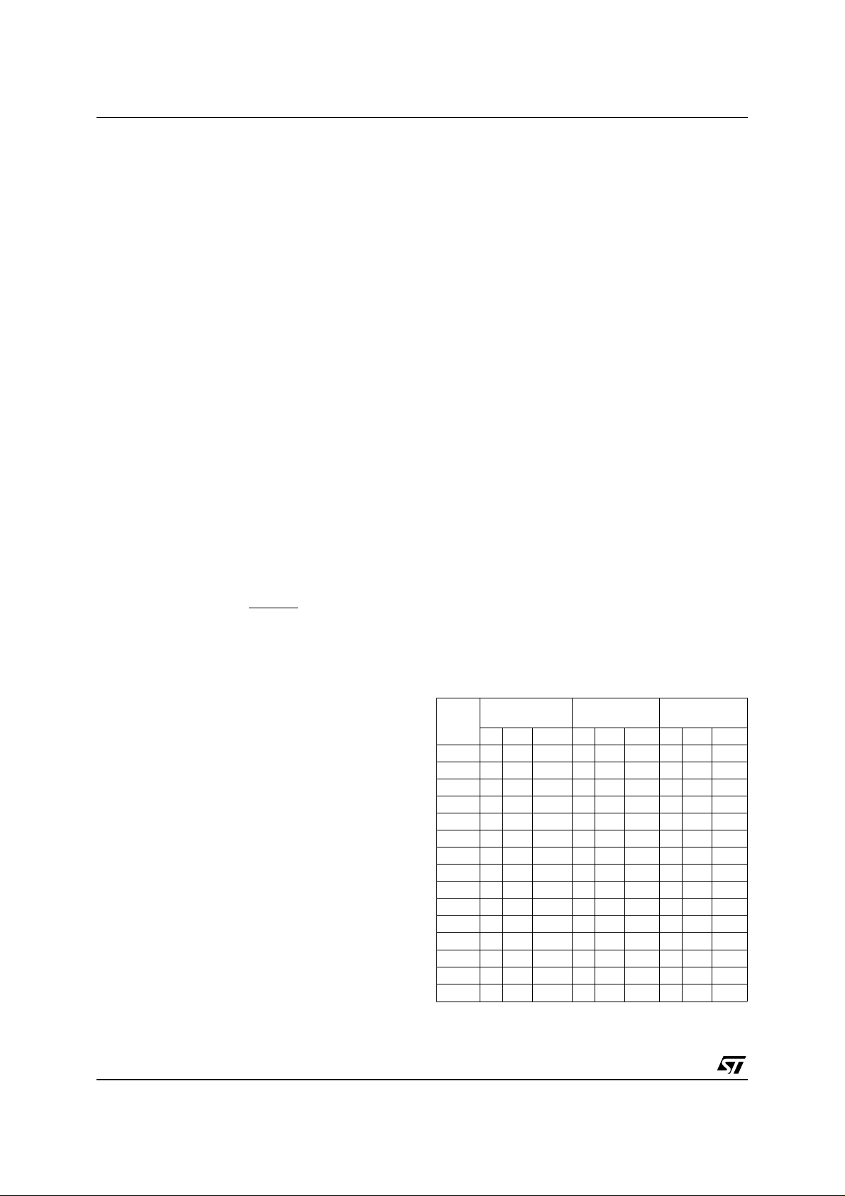
3 - CLOCK GENERA TOR
The master clock, MCLK is provided by the user
thanks to a crystal or e xternal clock generat or (see
Figur e 1) .
The MCLK could be equal to 36.864MHz
(MCM = 1). In that case thanks to the divider M x Q,
the STLC7550 is able to generate all V.34bis and
56 Kbps sampling frequencies (see Table 1).
When MCM = 0, the MCLK mu st be equal to the
oversampling frequency : Fs x OVER (7546 mode).
The ADC and DAC are oversampled at the OCLK
frequency. O CLK is equal to t he s hift clock used in
the serial interface.
The MCLK frequency should be :
MCLK = K x Sampling frequency
Combination of M, Q and oversampling ratios allows to generate several sampling frequencies.
Recommended values for classical modem applications are as follow :
Table 1 :
(kHz)
16.00 3 6 128 2 4.5 128 1 6 96
13.96 3 5.5 160 - - - - - -
13.71 3 7 128 1 7 192 1 7 96
12.80 3 6 160 2 4.5 160 1 4.5 160
12.00 3 8 128 2 6 128 1 6 128
11.82 3 6.5 160 - - - - - -
10.97 3 7 160 - - - - - -
10.47 4 5.5 160 2 5.5 160 1 5.5 160
10.29 4 7 128 2 7 128 1 7 128
9.60 4 6 160 2 6 160 1 6 160
9.00 4 8 128 2 8 128 1 8 128
8.86 4 6.5 160 2 6.5 160 1 6.5 160
8.23 4 7 160 2 7 160 1 7 160
8.00 4 6 192 2 6 192 1 6 192
7.20 4 8 160 2 8 160 1 8 160
Note :
Sampling Frequencies Generation
F
FQ =
36.864MHz (1)
M Q over M Q over M Q over
1. Recommended value.
FQ =
18.432MHz
FQ =
9.216MHz
6/17