

STLC60135
TOSCA
DTM modem for ADSL, compatible with the
followingstandards:
– ANSI T1.413 Issue 2
– ITU-T G.992.1(G.dmt)
– ITU-T G.992.2(G.lite)
Samechip for both ATU-C and ATU-R
Supportseither ATM (Utopia level1 & 2) or bit-
stream interface
16 bit multiplexed microprocessor interface (lit-
tle and bigendiancompatibility)
Analog Front End management
Dual latencypaths: fast and interleaved
ATM’s PHY layer: cell processing (cell deline-
ation, cell insertion,HEC)
ADSL’soverheadmanagement
Reed Solomonencode/decode
Trellis encode/decode(Viterbi)
DMT mapping/ demapping over 256 carriers
Fine (2ppm) timing recover using Rotor and
AdaptativeFrequencyDomainEqualizing
TimeDomain Equalization
Frontend digitalfilters
0.35µmHCMOS6Technology
144 pin PQFPpackage
PowerConsumption1 Watt at 3.3V
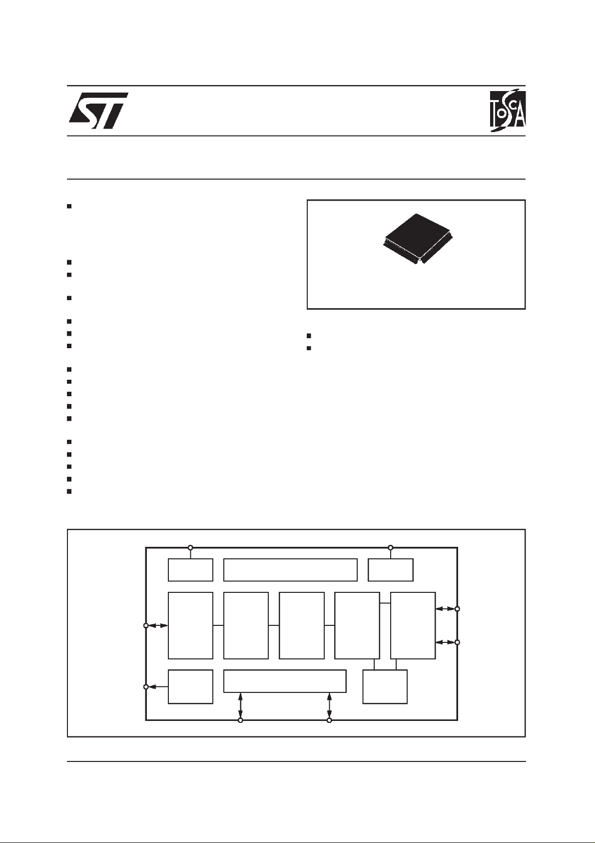
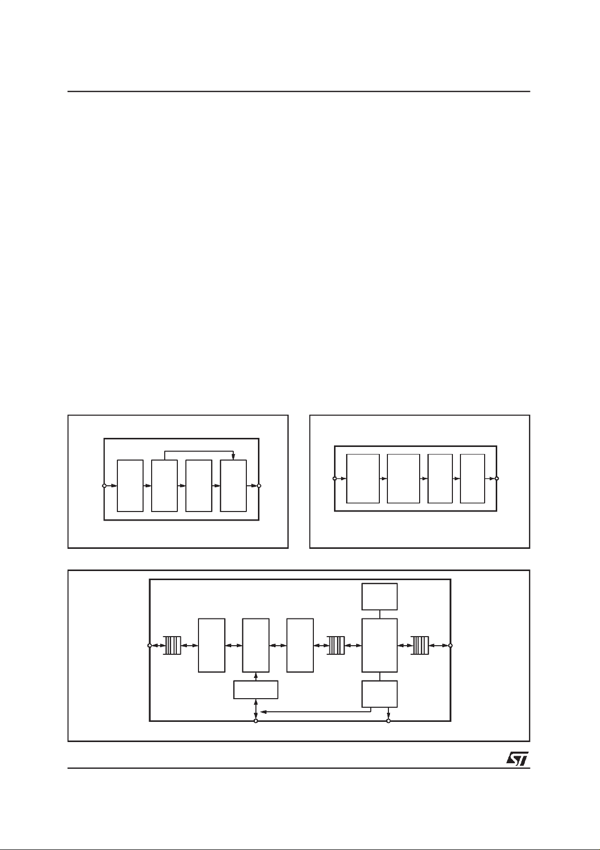
Figure 1. Block Diagram
ADSL DMT TRANSCEIVER
PQFP144
ORDERING NUMBER: STLC60135
Applications
ATU-C:
ATU-R:
DSLAM,Routersat Central Office
Routers at SOHO, stand-alone mo-
dems, PC motherboards
GeneralDescription
The STLC60135 is the DMT modem and ATM
framerof theSTMicroelectronicsTosca chipset.
When coupled with STLC60134 analog front-end
and an external controller running dedicated firmware, the product fulfils ANSI T1.413 “Issue 2”
DMT ADSL specification.
The STLC60135 may be used at both ends of
ADSL loop: ATU-C and ATU-R. The chip supports UTOPIA level 1 and UTOPIA level 2 interface and a non ATM synchronous bit-stream interface.
AFE
INTERFACE
AFE
CONTROL
September 1999
TEST SIGNALS CLOCK
TEST
MODULE
DSP
FRONT-END
AFE
CONTROL
INTERFACE
CONTROLLER BUS GENERAL PURPOSE I/Os
DATA SYMBOLTIMING UNIT VCXO
FFT/IFFT
ROTOR
CONTROLLER INTERFACE
TRELLIS
CODING
MAPPER/
DEMAPPER
GENERIC
TC
REED/
SOLOMON
ATM
SPECIFIC
TC
INTERFACE
MODULE
STM
UTOPIA
D98TL315
1/25
STLC60135
The STLC60135 can be splitted up into two different sections. The physical one performs the DMT
modulation, demodulation,Reed-Solomonencoding, bit interleavingand 4D trellis coding.
The ATM section embodies framing functions for
the generic and ATM Transmission Convergence
(TC) layers. The generic TC consists of data
scrambling and Reed Solomon error corrections,
with and without interleaving.
The STLC60135 is controlled and programmed
by an external controller (ADSL Transceiver Controller, ATC) that sets the programmable coefficients.
Transient Energy Capabilities
ESD
ESD (Electronic Discharged) tests have been
performed for the HumanBody Model (HBM) and
for the Charged Device Model (CDM).
The pins of the device are to be able to withstand
minimum 1500V for the HBM and minimum250V
for CDM.
Latch-up
The maximum sink or sourcecurrentfrom any pin
is limitedto 100mA to prevent latch-up.
The firmware controls the initialization phase and
carriesout the consequentadaptationoperations.
ABSOLUTE MAXIMUM RATINGS
Symbol Parameter Min Typ Max Unit
V
DD
P
tot
T
amb
Supply Voltage 3.0 3.3 3.6 V
Total Power Dissipation 900 1400 mW
Ambient Temperature 1m/s airflow -40 85 °C
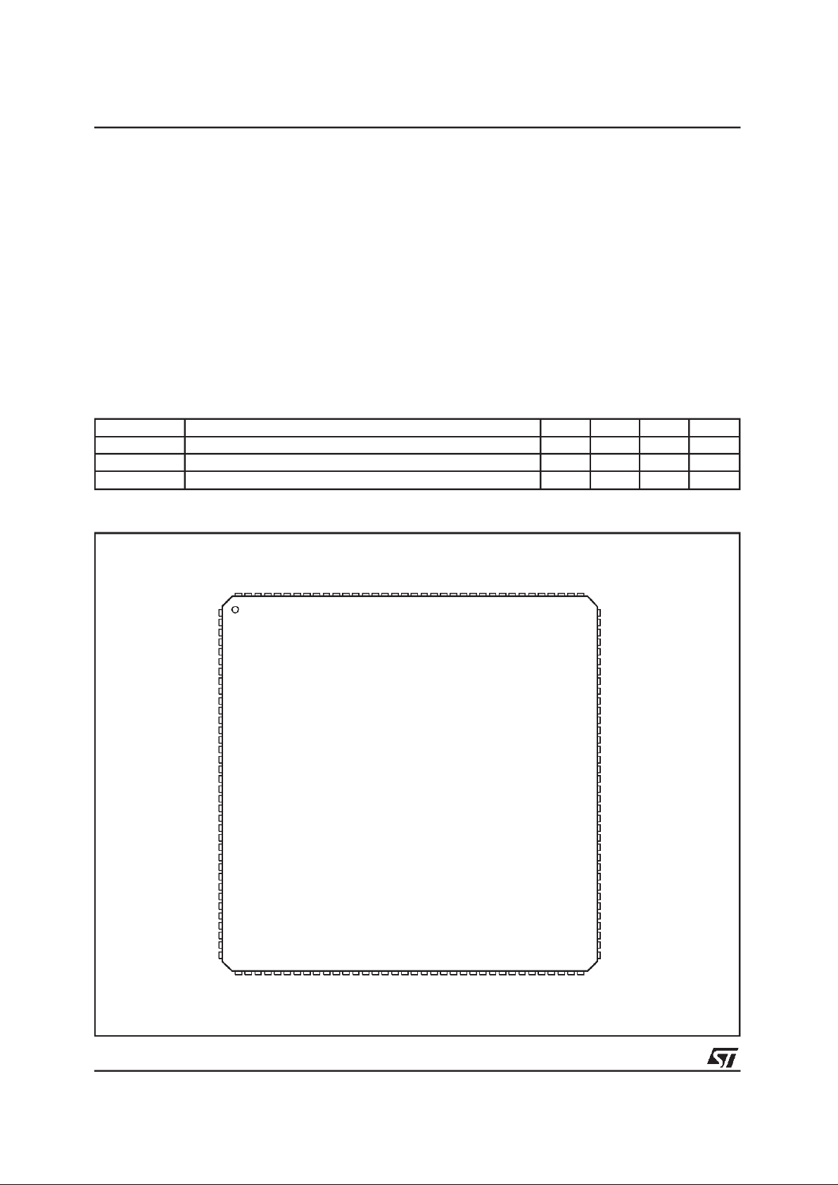
Figure 2. Pin Connection
AFTXD_0
IDDq
VDD
AFTXED_3
VSS
AFTXED_2
AFTXED_1
AFTXED_0
VDD
CTRLDATA
52 53
VDD
U_RXDATA_7
U_RX_ADDR_0
U_RX_ADDR_1
MCLK
CLWD
AFRXD_3
VSS
AFRXD_2
124 122123 121120119118117
54 55 56 57 58 59
VSS
GP_IN0
U_RX_ADDR_2
U_RX_ADDR_3
U_RX_ADDR_4
AFRXD_1
AFRXD_0
VDD
VSS
VDD
GP_IN1
PDOWN
GP_OUT
TESTSE
62 63 64 65 66 67
60 61
VDD
U_TX_REFB
U_RX_REFB
TRSTB
VSS
116 114115 113112111110109
U_RXCLK
U_RXSOC
AFTXD_1
VSS
AFTXD_2
AFTXD_3
VDDVDD
140
141
1
VSS
2
AD_0
3
AD_1
4
AD_2
5
VDD
6
AD_3
7
AD_4
8
VSS
9
AD_5
10
AD_6
VDD
12
AD_7
13
AD_8
14
AD_9
15
VSS
16
AD_10
17
AD_11
18
VDD
19
AD_12
20
VSS
21
PCLK
22
VDD
23
AD_13
24
AD_14
25
AD_15
26
VSS
27
BE1
28
ALE
29
VDD
30
CSB
31
WR_RDB
32
RDYB
OBC_TYPE
33
34
INTB
35
RESETB
36
VSS VSS
37 38 39 40
U_RXDATA_0
41 42 43 44 45
VSS
U_RXDATA_1
135134133132 130131 129128127126125
137142143144
138
139
136
461147 48 49 50 51
VSS
VDD
U_RXDATA_3
U_RXDATA_4
U_RXDATA_5
U_RXDATA_2
U_RXDATA_6
TCK
VDD
TMS
68 69 70
VSS
U_RXCLAV
U_RXENBB
TDI
TDO
U_TXCLK
U_TXSOC
SLT_FRAME_S
SLT_REQ_S
VSS
108
VDD
107
SLT_REQ_F
106
SLT_DAT_S0
105
SLT_DAT_S1
104
SLT_DAT_F0
103
SLT_DAT_F1
102
VSS
101
SLT_FRAME_F
100
SLAP_CLOCK
99
SLR_VAL_F
98
SLR_DAT_F0
97
SLR_DAT_F1
96
SLR_VAL_S
95
VDD
94
SLR_DAT_S0
93
SLR_DAT_S1
92
SLR_FRAME_S
91
VSS
90
SLR_FRAME_F
89
U_TX_ADDR_0
88
U_TX_ADDR_1
87
U_TX_ADDR_2
86
VDD
85
U_TX_ADDR_3
84
U_TX_ADDR_4
83
U_TX_DATA_0
82
U_TX_DATA_1
81
VDD
80
U_TX_DATA_2
79
U_TX_DATA_3
78
U_TX_DATA_4
77
U_TX_DATA_5
76
VDD
75
U_TX_DATA_6
74
U_TX_DATA_7
73
71
72
VDD
D98TL367B
U_TXENBB
U_TX_CLAV
2/25
PIN FUNCTIONS
Pin Name Type Supply Driver BS Function
1 VSS 0V Ground
2 AD_0 B VDD BD8SCR B Data 0
3 AD_1 B VDD BD8SCR B Data 1
4 AD_2 B VDD BD8SCR B Address / Data 2
5 VDD (V
6 AD_3 B VDD BD8SCR B Address / Data 3
7 AD_4 B VDD BD8SCR B Address / Data 4
8 VSS 0V Ground
9 AD_5 B VDD BD8SCR B Address / Data 5
10 AD_6 B VDD BD8SCR B Address / Data 6
11 VDD (V
12 AD_7 B VDD BD8SCR B Address / Data 7
13 AD_8 B VDD BD8SCR B Address / Data 8
14 AD_9 B VDD BD8SCR B Address / Data 9
15 VSS 0V Ground
16 AD_10 B VDD BD8SCR B Address / Data 10
17 AD_11 B VDD BD8SCR B Address / Data 11
18 VDD (V
19 AD_12 B VDD BD8SCR B Address / Data 12
20 VSS 0V Ground
21 PCLK I VDD IBUF I Processor clock
22 VDD (V
23 AD_13 B VDD BD8SCR B Address / Data 13
24 AD_14 B VDD BD8SCR B Address / Data 14
25 AD_15 B VDD BD8SCR B Address / Data 15
26 VSS 0V Ground
27 BE1 I VDD IBUF I Address 1
28 ALE I VDD IBUF C Address Latch
29 VDD (V
30 CSB I VDD IBUF I Chip Select
31 WR_RDB I VDD IBUF I Specifies the direction of the access cycle
32 RDYB OZ VDD BT4CR O Controls the ATC bus cycle termination
33 OBC_TYPE I-PD VDD IBUF I ATC Mode Selection (0 = i960; 1 = generic)
34 INTB O VDD IBUF O Requests ATC interrupt service
35 RESETB I VDD IBUF I Hard reset
36 VSS 0V Ground
37 VDD (V
38 U_RxData_0 OZ VDD BD8SRC B Utopia RX Data 0
39 U_RxData_1 OZ VDD BD8SRC B Utopia RX Data 1
40 VSS 0V Ground
41 U_RxData_2 OZ VDD BD8SRC B Utopia RX Data 2
42 U_RxData_3 OZ VDD BD8SRC B Utopia RX Data 3
43 VDD (V
+ 3.3V) Power Supply
SS
SS + 3.3V) Power Supply
SS + 3.3V) Power Supply
+ 3.3V) Power Supply
SS
SS + 3.3V) Power Supply
+ 3.3V) Power Supply
SS
+ 3.3V) Power Supply
SS
STLC60135
3/25
STLC60135
PIN FUNCTIONS (continued)
Pin Name Type Supply Driver BS Function
44 U_RxData_4 OZ VDD BD8SRC B Utopia RX Data 4
45 U_RxData_5 OZ VDD BD8SRC B Utopia RX Data 5
46 VSS 0V Ground
47 U_RxData_6 OZ VDD BD8SRC B Utopia RX Data 6
48 U_RxData_7 OZ VDD BD8SRC B Utopia RX Data 7
49 VDD (V
50 U_RxADDR_0 I VDD IBUF I Utopia RX Address 0
51 U_RxADDR_1 I VDD IBUF I Utopia RX Address 1
52 U_RxADDR_2 I VDD IBUF I Utopia RX Address 2
53 U_RxADDR_3 I VDD IBUF I Utopia RX Address 3
54 VSS 0V Ground
55 U_RxADDR_4 I VDD IBUF I Utopia RX Address 4
56 GP_IN_0 I-PD VDD IBUFDQ I General purpose input 0
57 VDD (V
58 GP_IN_1 I-PD VDD IBUFDQ I General purpose input 1
59 VSS 0V Ground
60 U_RxRefB O VDD IBUF O 8kHz clock to ATM device
61 U_TxRefB I VDD BT4CR I 8kHz clock from ATM device
62 VDD (V
63 U_Rx_CLK I VDD IBUF Utopia RX Clock
64 U_Rx_SOC OZ VDD BD8SCR Utopia RX Start of Cell
65 U_RxCLAV OZ VDD BD8SCR Utopia RX Cell Available
66 U_RxENBB I VDD IBUF Utopia RX Enable
67 VSS 0V Ground
68 U_Tx_CLK I VDD IBUF Utopia TX Clock
69 U_Tx_SOC I VDD IBUF Utopia TX Start of Cell
70 U_TxCLAV OZ VDD BD8SCR Utopia TX Cell Available
71 U_TxENBB I VDD IBUF Utopia TX Enable
72 VDD (V
73 VSS 0V Ground
74 U_TxData_7 I VDD IBUF I Utopia TX Data 7
75 U_TxData_6 I VDD IBUF I Utopia TX Data 6
76 VDD (V
77 U_TxData_5 I VDD IBUF I Utopia TX Data 5
78 U_TxData_4 I VDD IBUF I Utopia TX Data 4
79 U_TxData_3 I VDD IBUF I Utopia TX Data 3
80 U_TxData_2 I VDD IBUF I Utopia TX Data 2
81 VDD (V
82 U_TxData_1 I VDD IBUF I Utopia TX Data 1
83 U_TxData_0 I VDD IBUF I Utopia TX Data 0
84 U_TxADDR_4 I VDD IBUF I Utopia TX Address 4
85 U_TxADDR_3 I VDD IBUF I Utopia TX Address 3
86 VDD (V
87 U_TxADDR_2 I VDD IBUF I Utopia TX Address 2
88 U_TxADDR_1 I VDD IBUF I Utopia TX Address 1
89 U_TxADDR_0 I VDD IBUF I Utopia TX Address 0
90 SLR_ FRAME_F O VDD BT4CR Frame Identifier Fast
91 VSS 0V Ground
SS + 3.3V) Power Supply
+ 3.3V) Power Supply
SS
+ 3.3V) Power Supply
SS
SS + 3.3V) Power Supply
+ 3.3V) Power Supply
SS
+ 3.3V) Power Supply
SS
+ 3.3V) Power Supply
SS
4/25
PIN FUNCTIONS (continued)
Pin Name Type Supply Driver BS Function
92 SLR_FRAME_S O VDD BT4CR Receive Frame Identifier Interleaved
93 SLR_DATA_S_1 O VDD BT4CR Receive Data Interleave 1
94 SLR_DATA_S_0 O VDD BT4CR Receive Data Interleave 0
95 VDD (V
96 SLR_VAL_S O VDD BT4CR Receive Data Valid Indicator Interleaved
97 SLR_DATA_F_1 O VDD BT4CR Receive Data Fast 1
98 SLR_DATA_F_0 O VDD BT4CR Receive Data Fast 0
99 SLR_VAL_F O VDD BT4CR Receive Data Valid Indicator Fast
100 SLAP_CLOCK O VDD BT4CR Clock for SLAP I/F
101 SLT_FRAME_F O VDD BT4CR Transmit Start of frame Indicator Fast
102 VSS 0V Ground
103 SLT_DATA_F_1 I VDD IBUFDQ Transmit Data Fast 1
104 SLT_DATA_F_0 I VDD IBUFDQ Transmit Data Fast 0
105 SLT_DATA_S_1 I VDD IBUFDQ Transmit Data Interleave 1
106 SLT_DATA_S_0 I VDD IBUFDQ Transmit Data Interleave 0
107 SLT_REQ_F O VDD BT4CR Transmit Byte Request Fast
108 VDD (V
109 VSS 0V Ground
110 SLT_REQ_S O VDD BT4CR Transmit Byte Request Interleaved
111 STL_FRAME_S O VDD BT4CR Transmit Start of frame Indication Interleaved
112 TDI I-PU VDD IBUFUQ JTAG I/P
113 TDO OZ VDD BT4CR JTAG O/P
114 TMS I-PU VDD IBUFUQ JTAG Made Select
115 VDD (V
116 TCK I-PD VDD IBUFDQ JTAG Clock
117 VSS 0V Ground
118 TRSTB I-PD VDD IBUFDQ JTAG Reset
119 TESTSE I VDD IBUF none Enables scan test mode
120 GP_OUT O VDD BD8SCR O General purpose output
121 PDOWN O VDD BT4CR O Power down analog front end (Reset)
122 VDD (V
123 AFRXD_0 I VDD IBUF I Receive data nibble
124 AFRXD_1 I VDD IBUF I Receive data nibble
125 AFRXD_2 I VDD IBUF I Receive data nibble
126 AFRXD_3 I VDD IBUF I Receive data nibble
127 VSS 0V Ground
128 CLWD I VDD IBUF I Start of word indication
129 MCLK I VDD IBUF C Master clock
130 CTRLDATA O VDD BT4CR O Serial data Transmit channel
131 VDD (V
132 AFTXED_0 O VDD BT4CR O Transmit echo nibble
133 AFTXED_1 O VDD BT4CR O Transmit echo nibble
134 VSS 0V Ground
135 AFTXED_2 O VDD BT4CR O Transmit echo nibble
136 AFTXED_3 O VDD BT4CR O Transmit echo nibble
137 VDD (V
138 IDDq I VDD IBUF none Testpin, active high
SS + 3.3V) Power Supply
+ 3.3V) Power Supply
SS
SS + 3.3V) Power Supply
+ 3.3V) Power Supply
SS
+ 3.3V) Power Supply
SS
SS + 3.3V) Power Supply
STLC60135
5/25
STLC60135
PIN FUNCTIONS (continued)
Pin Name Type Supply Driver BS Function
139 AFTXD_0 O VDD BT4CR O Transmit data nibble
140 AFTXD_1 O VDD BT4CR O Transmit data nibble
141 VSS 0V Ground
142 AFTXD_2 O VDD BT4CR O Transmit data nibble
143 AFTXD_3 O VDD BT4CR O Transmit data nibble
144 VDD (V
I/O DRIVER FUNCTION
Driver Function
BD4CR CMOS bidirectional, 4mA, slew rate control
BD8SCR CMOS bidirectional, 8mA, slew rate control, Schmitt trigger
IBUF CMOS input
IBUFDQ CMOS input, pull down, IDDq control
IBUFUQ CMOS input, pull up, IDDq control
PIN SUMMARY
Mnemonic Type BS Type Signals Function
SS + 3.3V) Power Supply
Power Supply
VDD (VSS+ 3.3V) Power Supply
VSS 0V Ground
ATC Interface
ALE I C 1 Used to latch the address of the internal register to be accessed
PCLK I I 1 Processor clock
CSB I I 1 Chip selected to respond to bus cycle
BE1 I I 1 Address 1 (notmultiplexed)
WR_RDB I I 1 Specifies the direction of the access cycle
RDYB OZ O 1 Controls the ATC bus cycle termination
INTB O O 1 Requests ATC interrupt service
AD IO B 16 MultiplexedAddress/Data bus
OBC_TYPE I-PD I 1 Select betweeni960 (0) or generic (1) controller interface
Test Access Part Interface
TDI I-PU 1 refer to section
TDO OZ 1
TCK I-PD 1
TMS I-PU 1
TRSTB I-PD 1
Analog Front End Interface
AFRXD I I 4 Receive data nibble
AFTXD O O 4 Transmit data nibble
AFTXED O O 4 Transmit echo nibble
CLWD I I 1 Start of word indication
PDOWN O O 1 Power down analog front end
CTRLDATA O O 1 Serial data transmit channel
MCLK I C 1 Master clock
6/25
PIN SUMMARY(continued)
Mnemonic Type BS Type Signals Function
ATM UTOPIA Interface
U_RxData OZ B 8 Receive interface Data
U_TxData I I 8 Transmit interface Data
U_RxADDR I I 5 Receive interface Address
U_TxADDR I I 5 Transmit interface Address
U_RxCLAV OZ O 1 Receive interface Cell Available
U_TxCLAV OZ O 1 Transmit interface Cell Available
U_RxENBB I-TTL I 1 Receive interface Enable
U_TxENBB I-TTL I 1 Transmit interface Enable
U_RxSOC OZ O 1 Receive interface Start of Cell
U_TxSOC I-TTL I 1 Transmit interface Start of Cell
U_RxCLK I-TTL C 1 Receive interface Utopia Clock
U_TxCLK I-TTL C 1 Transmit interface Utopia Clock
U_RxRefB O O 1 8kHz reference clock to ATM device
U_TxRefB I-TTL I 1 8kHz reference clock from ATM device
ATM SLAP Interface
SLR_VAL_S O 1
SLR_VAL_F O 1
SLR_DATA_S O 2
SLR_DATA_F O 2
SLT_REQ_S O 1
SLT_REQ_F O 1
SLT_DATA_S I 2
SLT_DATA_F I 2
SLAP_CLOCK O 1
SLR_FRAME_I O 1
SLT_FRAME_I O 1
SLR_FRAME_F O 1
SLT_FRAME_F O 1
STLC60135
Miscellaneous
GP_IN I-PD I 2 General purpose input
GP_OUT O O 1 General purpose output
RESETB I I I Hard reset
TESTSE I none none Enable scan test mode
IDDq I none none Test pin, active high
I = Input, CMOS levels
I-PU = Input with pull-up resistance, CMOS levels
I-PD = Input with pull-down resistance, CMOS levels
I-TTL = Input TTL levels
O = Push-pull output
OZ = Push-pull output with high-impedance state
IO = Input / Tristate Push-pull output
BS cell = Boundary-Scan cell
I = Input cell
O = Output cell
B = Bidirectional cell
C = Clock
7/25
STLC60135
Main Block Description
The following drawings describe the sequence of
functionsperformed by the chip.
DSP Front-End
The DSP Front-End contains 4 parts in the receive direction: the Input Selector, the Analog
Front-End Interface, the Decimator and the Time
Equalizer. The input selector is used internally to
enable testloopbacksinside the chip. The Analog
Front-End lnterface transfers 16-bit words, multiplexed on 4 input/outputsignals. Word transfer is
carried out in 4 clock cycles.
The Decimator receive 16-bits samples at 8.8
MHz (as sent by the Analog Front-End chip:
STLC60134) and reducesthis rate to 2.2 MHz.
The Time Equalizer (TEQ) module is a FIR filter
with programmablecoefficients. Its main purpose
is to reduce the effect of Inter-Symbol Interferences (ISI) by shortening the channel impulse response.
Both the Decimatorand TEQ can be bypassed.
In the transmit direction, the DSP Front-End in-
cludes: sidelobe filtering, clipping, delay equalization and interpolation. The sidelobe filtering and
Figure 3. DSP Front-End Receive
delay equalizationare implemented by IIR Filters,
reducing the effect of echo in FDM systems.Clipping is a statistical process limiting the amplitude
of the output signal, optimizingthe dynamicrange
of the AFE. The interpolator receives data at 2.2
MHz and generates samples at a rate of 8.8
MHz.
DMT Modem
This module is a programmable DSP unit. Its instruction set enables the basic functions of the
DMT algorithm like FFT, IFFT, Scaling, Rotor and
Frequency Equalization(FEQ) in compliance with
ANSI T1.413 specifications.
In the RX path, the 512-point FFT transforms the
time-domain DMT symbol into a frequency domain representation which can be further decoded by the subsequentdemapping stages.
In other words, the Fast Fourier Transform process is used to transform from time domain to frequency domain (receive path). On ATU-C side,
128 time samples are processed. On ATU-R side,
1024 timesamplesare processed.
After the first stage time domain equalization and
FFT block an ICI (InterCarrier Interference) free
informationstream turns out.
Figure 4. DSP Front-End Transmit
BYPASS
FROM
ANALOG
FRONT-END
IN
SELECT
AFE
I/F
DEC TEQ
Figure 5. DMT Modem (Rx & Tx)
TO/FROM
DSP FE
FFT
IFFT
TO DMT
MODEM
D98TL372A
FEQ
FTG
FEQ
COEFFICIENTS
FEQ
UPDATE
ROTOR
FROM
DMT
MODEM
Filtering
Clipping
Delay
Equalizer
TRELLIS
CODING
DECODING
MAPPER
DEMAPPER
MONITOR
MONITOR
INDICATIONS
Interpolator
AFE
I/F
D98TL316A
OUT
SELECT
TO/FROM
TC
D98TL382
TO ANALOG
FRONT END
8/25
 Loading...