STLC60133
XDSL LINE DRIVER
PRELIMINARY DATA
■
LOW NOISE : 4nV/
■
HIGH PEAK OUTPUT CURRENT: 500 mA
■
HIGH SPEED
Hz
– 140MHz Gain Bandwidth
– 30MHz Gain Flatness
– 400 V/us Slew Rate
■
LOW POWER OPERATION
– ±5V to ±15V Voltage Supply
– 12.5 mA/Amp (typ) Supply current
– Power reduced Current
■
LOW SINGLE TONE DISTORTION
■
THERMAL AND OVERLO AD PROTECTION
■
HTSSOP28 PACKAGE
■
-40 TO +85°C OPERATING RANGE
DESCRIPTION
The STLC60133 is a dual amplifier featuring a high
slew rate and a large bandwidth optimized for XDSL
applications. The dev ice is avai lable in a HTSSOP 28
pin package (4x9 mm) with an exposed leadframe.
Thanks to its small pack age thi s l ine driv er is sui table
for high density ADSL line card.
HTSSOP28
ORDERING NUMBER: STLC60133
Temperature Range: -40°C to +85°C
Two digital pins (PWDN0 and PWDN1) allow the driver to work in full performance mode, in low-power
mode or two intermediate bias states.
The low-power mode biases the output stage in or der
to provide a low impedance at the amplifier outputs
for back termination.
The STLC60133 is designed optimizing bandwidth
and distortion perfor mances . For p roper devic e operating it is necessary to work with a gain level greater
than 15.6dB.
Typical differential gain is normally +27dB, while typical common mode gain is 15.6dB
Figure 1. BLOCK DIAGRAM
-V
+V
S
S
Op1
IN1N
IN1P
PWDN0
PWDN1
BIAS
DGND
IN2N
IN2P
October 2001
This is preliminary information on a new product now in development. Details are subject to change without notice.
LOGIC
-
+
-
+
Op2
OUT1
TH DETCT.
OUT2
D00TL462A
1/9

STLC60133
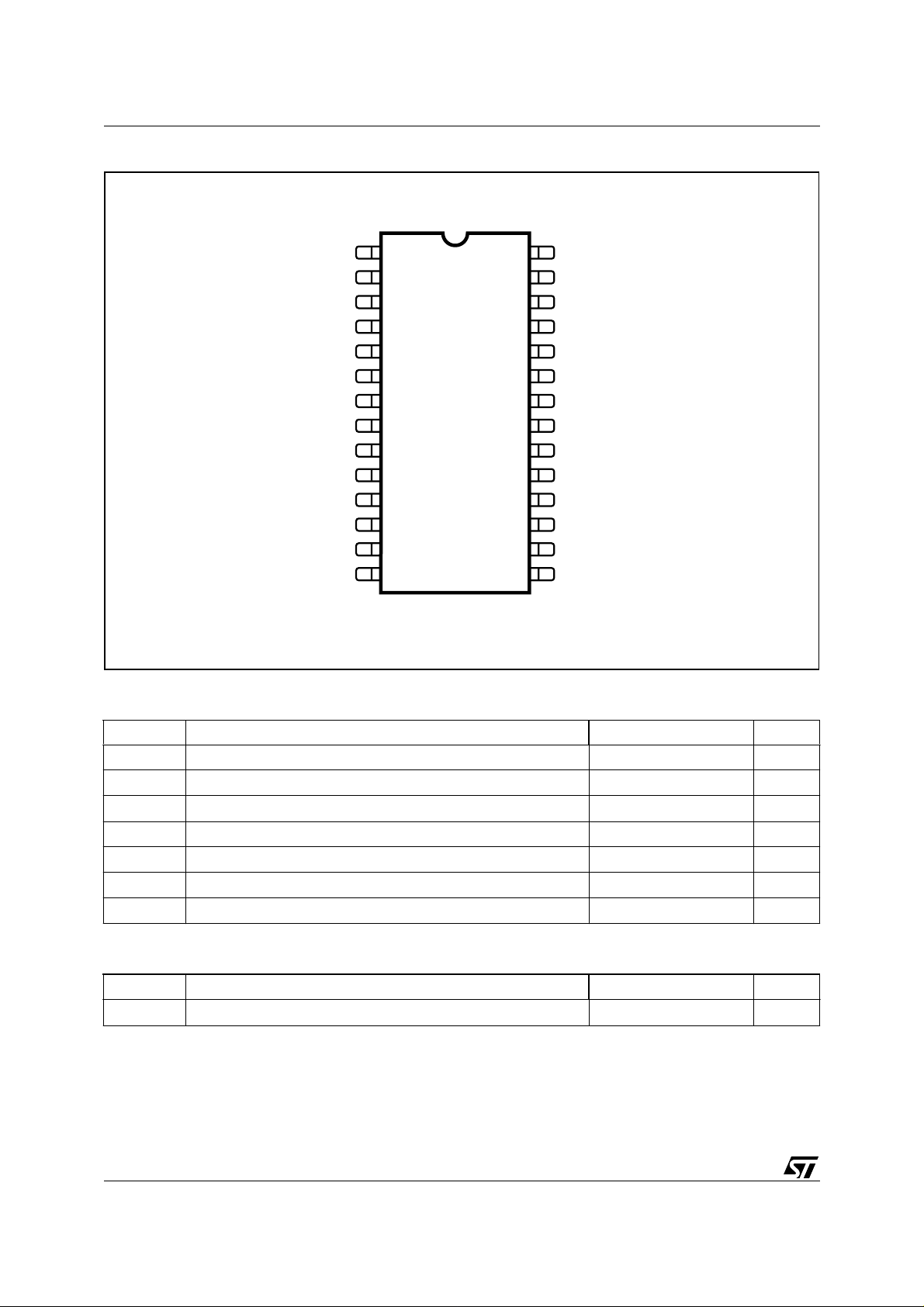
PIN CONNECTION
RES
N.C.
N.C.
IN2P
IN2N
OUT2
+V
S
+V
S
OUT1 DGND
IN1N N.C.
2
3
4
5
6
7
8
9
10
IN1P
N.C
N.C. N.C.
12
13
28
27
26
25
24
23
22
21
20
19
18
17
16
RES1
N.C.
N.C.
N.C.
PWDN1
BIAS
-V
S
-V
S
PWDN011
N.C.
1514N.C. N.C.
D00TL463A
ABSOLUTE MAXIMUM RATINGS
Symbol Parameter Value Unit
V
CC
V
SS
V
id
V
T
op
T
stg
T
Positive Supply voltage (note1) +16.5 V
Negative Supply voltage (note1) -16.5 V
Differential Input Voltage (note2) ±5 V
Common mode Input Voltage ±1 V
i
Operating Free Air Temperature Range -40 to +85 °C
Storage temperature -65 to +150 °C
Junction temperature 150 °C
j
THERMAL DATA
Symbol Parameter Value Unit
R
thj-amb
Thermal resistance junction to ambient (note 3) 29 °C/W
2/9

STLC60133
OPERATING RANGE
Symbol Parameter Value Unit
T
op
V
CC
V
SS
V
DGND
V
icm
Notes
1) All voltag es values , except differential voltage , are with re spect to netw ork ground term i nal .
2) Differential volt ages are non-inverting in put terminal with resp ect to the inverting inp ut termina l
3) Specification is for device on a 4 layer board within 10 square inches of oz. copper at +85°C and 200m/s air velocity. With 0m/s air velocity
the parameter incre ases up to 33° C/ W
.
PIN DESCRIPTION
2, 3, 12, 13, 14,
15, 16, 17, 19,
25, 26, 27
21, 22 -Vs Negative Supply Voltage
Operating Temperature Range -40 to 85 °C
Positive Supply voltage (note1) +5 to +15 V
Negative Supply voltage (note1) -5 to -15 V
Digital Ground level VSS+5<V
DGND<VCC
Common Mode Input Voltage Range ±1 V
N° Pin Description
NC Not Connected
4 IN2P Non Inverting Input of Op. Amplifier 2
5 IN2N Inverting Input of Op. Amplifier 2
6 OUT2 Ouput of Op. Amplifier 2
7, 8 +Vs Positive Supply Voltage
9 OUT1 Ouput of Op. Amplifier 1
10 IN1N Inverting Input of Op. Amplifier 1
11 IN1P Non Inverting Input of Op. Amplifier 1
14 PWDN1 Power Down 1 logic input
18 PWDN0 Power Down 0 logic input
23 BIAS Bias Control pin
1, 28 RES To be left not connected
-5 V
Power Down Management
The STLC60133 provides several quiescent bias levels from full performance, to reduced bias (in three steps
through PWDN0/1 pins) or to full OFF operation (through BIAS pin). According to the different XDSL application
(both site CO and CPE), different bias levels can be chosen maintaining good MTPR performances. In the following table are shown the bias levels versus the PWDN values.
PWDN1 PWDN0 Bias Level
1 1 100%
1 0 60%
0 1 40%
0 0 25% (low Zout but not OFF)
X X Full OFF (High Zout via 250uA pulled out of BIAS pin)
3/9
 Loading...