

STLC5465B
MULTI-HDLC
WITH n x 64SWITCHINGMATRIX ASSOCIATED
November 1999
PQFP160
(Plastic Quad Flat Pack)
ORDERING NUMBER : STLC5465B
.
32 TxHDLCs WITH BROADCASTING CAPABILITY AND/OR CSMA/CR FUNCTION WITH
AUTOMATIC RESTART IN CASE OF TX
FRAMEABORT
.
32 RxHDLCs INCLUDING ADDRESS RECOGNITION
.
16 COMMAND/INDICATE CHANNELS (4 OR
6-BITPRIMITIVE)
.
16 MONITOR CHANNELS PROCESSED IN
ACCORDANCE WITH GCI OR V*
.
256 x 256 SWITCHING MATRIX WITHOUT
BLOCKING AND WITH TIME SLOT SEQUENCE INTEGRITY AND LOOPBACK PER
BIDIRECTIONALCONNECTION
.
DMA CONTROLLER FOR 32 Tx CHANNELS
AND32 Rx CHANNELS
.
HDLCs AND DMA CONTROLLER ARE CAPABLE OF HANDLING A MIX OF LAPD, LAPB,
SS7,CASANDPROPR IETAR YSIGNALLINGS
.
EXTERNALSHARED MEMORYACCESSBETWEEN DMA CONTROLLER AND MICROPROCESSOR
.
SINGLE MEMORY SHARED BETWEEN
nx
MULTI-HDLC
s AND SINGLE MICROPROCESSOR ALLOWS TO HANDLE n x 32
CHANNELS
.
BUSARBITRATION
.
INTERFACE FOR VARIOUS 8,16 OR 32 BIT
MICROPROCESSORS
.
RAM CONTROLLER ALLOWS TO INTERFACEUPTO :
-16MEGABYTESOF DYNAMIC RAM OR
-1 MEGABYTEOF STATIC RAM
.
INTERRUPT CONTROLLER TO STORE
AUTOMATICALLY EVENTS IN SHARED
MEMORY
.
PQFP160PACKAGE
.
BOUNDARY SCAN FOR TEST FACILITY
DESCRIPTION
TheSTLC5465Bis a Subscriberline interfacecard
controller for Central Office, Central Exchange,
NT2 and PBX capable of handling:
- 16 U Interfacesor
- 2 Megabitsline interfacecardsor
- 16 SLICs (PlainOld TelephoneService)or
- Mixed analogue and digital Interfaces(SLICs or
U Interfaces)or
- 16 S Interfaces
- Switching Network with centralized processing
1/101

TABLEOF CONTENTS Page
I - PIN INFORMATION ........................................ . 8
I.1 - PinConnections . . . . . . . . . . . . ............................ 8
I.2 - PinDescription . . . . . . . ................................. . 9
I.3 - PinDefinition . . . . . . . . . . . . ............................ ..13
I.3.1- Input Pin Definition . . . . . . . . . . . . ..........................13
I.3.2 - Output Pin Definition . . . . . . . ..............................13
I.3.3 - Input/OutputPin Definition . . . . . . . . . . ........................13
II - BLOCK DIAGRAM ........................................ .14
III - FUNCTIONAL DESCRIPTION ...................................15
III.1- The Switching Matrix N x 64 KBits/S . . . . . . .......................15
III.1.1 - Function Description . . . . . . . . . . . . . . . . . . . . . . . .............15
III.1.2 - Architectureof the Matrix . . . . . . . . . . ........................15
III.1.3 - ConnectionFunction . . . . . . . . . . . . . . . . . . . . . . . .............15
III.1.4 - Loop Back Function . . . . . . . ..............................15
III.1.5 - Delay through the Matrix . . . . . . . . . . ........................17
III.1.5.1- VariableDelayMode . . . . . . . ............................17
III.1.5.2 - SequenceIntegrity Mode . . . . . . . ..........................17
III.1.6 - ConnectionMemory . . . . . . . ..............................21
III.1.6.1- Description . . . . . . . . . . . . ............................21
III.1.6.2 - Accessto ConnectionMemory . . . . . . . . . . . . . . . . . . . . . . . .......21
III.1.6.3 - Accessto Data Memory . . . . . . . . . . ........................21
III.1.6.4 - Switchingat 32 Kbit/s . . . . . . . ............................21
III.1.6.5 - Switchingat 16 kbit/s . . . . . . . ............................21
III.2 - HDLC Controller . . . . . . . . . . . . ............................25
III.2.1- FunctionDescription . . . . . . . . . . . . . . . . . . . . . . . .............25
III.2.1.1 - Formatof the HDLC Frame . . . . . . . . . . . . . ...................25
III.2.1.2 - Compositionof an HDLC Frame . . . . . . .......................25
III.2.1.3 - Descriptionand Functionsof the HDLC Bytes . . . . . . . . . . . . . .........26
III.2.2 - CSMA/CRCapability . . . . . . . . . . . . . . . . . . . . . . . .............26
III.2.3 - Time Slot AssignerMemory . . . . . . . ..........................27
III.2.4 - Data Storage Structure . . . . . . . ............................27
III.2.4.1 - Reception . . . . . . . ................................. .27
III.2.4.2 - Transmission . . . . . . . ................................27
III.2.4.3 - FrameRelay . . . . . . . ................................27
III.2.5 - TransparentModes . . . . . . . ..............................29
III.2.6 - Commandof the HDLC Channels . . . . . . .......................29
III.2.6.1 - ReceptionControl . . . . . . . ..............................29
III.2.6.2 - Transmission Control . . . . . . . ............................29
III.3 - C/I and Monitor . . . . . . . . . . . . ............................29
III.3.1- FunctionDescription . . . . . . . . . . . . . . . . . . . . . . . .............29
III.3.2 - GCI and V* Protocol . . . . . . . ..............................30
III.3.3 - Structureof the Treatment . . . . . . . ..........................30
STLC5465B
2/101

TABLEOF CONTENTS (continued) Page
III - FUNCTIONAL DESCRIPTION(continued)
III.3.4 - CI and MonitorChannelConfiguration . . . ........................30
III.3.5 - CI and MonitorTransmission/ReceptionCommand . . . . . . . . . . . . . .......30
III.4 - MicroprocessorInterface . . . . . . . ............................34
III.4.1- Description . . . . . . . ................................. .34
III.4.2 - Exchangewith the sharedmemory . . . . . . .......................35
III.4.2.1 - WriteFIFO . . . . . . . . . . . . ............................35
III.4.2.2 - Read Fetch Memory . . . . . . . ............................35
III.4.3 - Definition of the Interfacefor the different microprocessors . . . . .............35
III.5 - Memory Interface . . . . . . . ................................38
III.5.1 - Function Description . . . . . . . . . . . . . . . . . . . . . . . .............38
III.5.2 - Choiceof memoryversus microprocessorand capacityrequired . . . . .........38
III.5.3 - MemoryCycle . . . . . . . ................................38
III.5.4 - SRAM interface . . . . . . . ................................39
III.5.5 - DRAM Interface . . . . . . . ................................39
III.5.4.2 - 512K x n SRAM . . . . . . . . . . . . ..........................39
III.5.5.2 - 1M x n DRAM Signals . . . . . . . ............................40
III.5.5.3 - 4M x n DRAM Signals . . . . . . . ............................40
III.6 - Bus Arbitration . . . . . . . . . . . . ............................40
III.7 - Clock Selection and Time Synchronization . . . . . . . . . . . . . .............41
III.7.1- Clock DistributionSelectionand Supervision . . . . ....................41
III.7.2 - VCXOFrequencySynchronization . . . . . . .......................41
III.8 - Interrupt Controller . . . . . . . . . . . . ..........................42
III.8.1- Description . . . . . . . ................................. .42
III.8.2 - Operating Interrupts (INT0 Pin) . . . . . . . . . . . . . . .................42
III.8.3 - Time Base Interrupts (INT1 Pin) . . . . . . . . . . . . . . . . . . . . . . . .......42
III.8.4 - EmergencyInterrupts(WDO Pin) . . . . . . . . . . . . . . . . . . . . . . . .......42
III.8.5 - Interrupt Queues . . . . . . . . . . . . ..........................42
III.9 - Watchdog . . . . . . . ................................. ...43
III.10 - Reset . . . . . . . . . . .............................. .....43
III.11 - BoundaryScan . . . . . . . ................................43
IV- DC SPECIFICATIONS .......................................44
IV.1 - Absolute Maximum Ratings . . . . . . . . . . ........................44
IV.2 - Power Dissipation . . . . . . . ................................44
IV.3 - RecommendedDC OperatingConditions . . . . . . . . . . . . . .............44
IV.4 - TTL Input DC ElectricalCharacteristics. . . . . . . . . ...................44
IV.5 - CMOS Output DC ElectricalCharacteristics . . . . . . . . . . . . . . ...........44
IV.6 - Protection . . . . . . . ................................. ...44
V - CLOCK TIMING ........................................ ...45
V.1 - SynchronizationSignals delivered by the system . . . . ...................45
V.2 - TDMSynchronization . . . . . . . ..............................46
V.3 - GCIInterface . . . . . . . ................................. .47
V.4 - V*Interface . . . . . . . . . . . . ............................ ..48
STLC5465B
3/101

TABLEOF CONTENTS (continued) Page
V1 - MEMORYTIMING ........................................ .49
VI.1 - Dynamic Memories . . . . . . . . . . . . ..........................49
VI.2 - Static Memories . . . . . . . . . . . . ............................51
VII - MICROPROCESSOR TIMING ...................................53
VII.1 - ST9 Family MOD0=1,MOD1=0,MOD2=0 . . . . . . . . . . . . . .............53
VII.2- ST10/C16xmult.A/D, MOD0 = 1, MOD1 = 0, MOD2 = 1 . . . . . . . . . . . . . .....55
VII.3- ST10/C16xdemult.A/D, MOD0 = 1, MOD1 = 0, MOD2= 1 . . . . .............57
VII.4 - 80C188 MOD0=1, MOD1=1,MOD2=0 . . . . . . . . . ...................59
VII.5 - 80C186 MOD0=1, MOD1=1,MOD2=1 . . . . . . . . . ...................61
VII.6 - 68000 MOD0=0, MOD1=0, MOD2=1 . . . . . . . . . ...................63
VII.7- 68020MOD0=0,MOD1=0,MOD2=0 . . . . . . . ......................65
VII.8 - Token Ring Timing . . . . . . . . . . . . ..........................67
VII.9 - MasterClock Timing . . . . . . . ..............................67
VIII - INTERNALREGISTERS .....................................68
VIII.1 - Identificationand Dynamic CommandRegister- IDCR(00)H ................68
VIII.2 - GeneralConfiguration- GCR (02)H .............................68
VIII.3 - Input MultiplexConfigurationRegister0 - IMCR0(04)H ..................70
VIII.4 - Input MultiplexConfigurationRegister1 - IMCR1(06)H ..................70
VIII.5 - Output Multiplex ConfigurationRegister0 - OMCR0 (08)H .................71
VIII.6 - Output Multiplex ConfigurationRegister1 - OMCR1 (0A)H .................71
VIII.7 - SwitchingMatrix ConfigurationRegister- SMCR (0C)H ..................71
VIII.8 - ConnectionMemoryData Register- CMDR(0E)H .....................74
VIII.9 - ConnectionMemoryAddressRegister- CMAR (10)H ...................77
VIII.10- SequenceFault Counter Register - SFCR (12)H .....................79
VIII.11- TimeSlot AssignerAddressRegister- TAAR (14)H ....................79
VIII.12- TimeSlot AssignerData Register - TADR(16)H .....................80
VIII.13- HDLCTransmit Command Register- HTCR(18)H ....................81
VIII.14- HDLCReceive Command Register - HRCR (1A)H ....................82
VIII.15- AddressField Recognition Address Register - AFRAR (1C)H ...............84
VIII.16- AddressField Recognition Data Register- AFRDR(1E)H .................84
VIII.17- Fill Character Register - FCR (20)H ............................84
VIII.18- GCI Channels Definition Register 0 - GCIR0 (22)H ....................84
VIII.19- GCI Channels Definition Register 1 - GCIR1 (24)H ....................85
VIII.20- GCI Channels Definition Register 2 - GCIR2 (26)H ....................85
VIII.21- GCI Channels Definition Register 3 - GCIR3 (28)H ....................85
VIII.22- TransmitCommand/ Indicate Register - TCIR (2A)H ...................86
TransmitCommand/Indicate Register (after reading) . . . . ...............86
VIII.23- TransmitMonitor Address Register - TMAR (2C)H ....................87
TransmitMonitorAddressRegister (after reading) . . . . .................87
VIII.24- TransmitMonitor Data Register- TMDR (2E)H ......................88
VIII.25- TransmitMonitor Interrupt Register - TMIR (30)H .....................88
VIII.26- Memory Interface ConfigurationRegister - MICR (32)H ..................88
Memory . . . . . . . . . . . . ............................ ..89
STLC5465B
4/101

TABLEOF CONTENTS (continued) Page
VIII - INTERNALREGISTERS(continued)
VIII.27- InitiateBlock Address Register - IBAR (34)H .......................90
VIII.28- InterruptQueue Size Register - IQSR (36)H ........................90
VIII.29- InterruptRegister- IR (38)H ................................91
VIII.30- InterruptMask Register - IMR (3A)H ............................92
VIII.31- Timer Register - TIMR (3C)H ...............................92
VIII.32- Test Register - TR (3E)H ..................................92
IX- EXTERNALREGISTERS ......................................93
IX.1 - InitializationBlock in ExternalMemory . . . . . . . . . ...................93
IX.2 - Receive Descriptor . . . . . . . . . . . . ..........................94
IX.2.1 - Bits written by the Microprocessoronly . . . ........................94
IX.2.2 - Bits written by the Rx DMAConly . . . . . . . . . . . . . . . . . . . . . . . .......94
IX.2.3 - ReceiveBuffer . . . . . . . ................................94
IX.3 - Transmit Descriptor . . . . . . . . . . . . ..........................95
IX.3.1 - Bits written by the Microprocessoronly . . . ........................95
IX.3.2 - Bits written by the DMAC only . . . . . . . . . . . . . . .................96
IX.3.3 - Transmit Buffer . . . . . . . ................................96
IX.4 - Receive & Transmit HDLC FrameInterrupt . . . . . . . . . . . . . .............96
IX.5 - Receive Command / IndicateInterrupt . . . . . . . . . ...................97
IX.5.1- ReceiveCommand/ IndicateInterruptwhen TSV = 0 . . . . ...............97
IX.5.2 - ReceiveCommand/ Indicate Interrupt when TSV = 1 . . . . ...............98
IX.6 - Receive Monitor Interrupt . . . . . . . ............................98
IX.6.1- ReceiveMonitorInterruptwhen TSV = 0 . . . . . . . . . . . . . .............98
IX.6.2 - ReceiveMonitor Interrupt when TSV = 1 . . . . . . . . . . . . . .............99
X - PQFP160PACKAGE MECHANICAL DATA ...........................100
STLC5465B
5/101

LIST OF FIGURES Page
I - PIN INFORMATION ........................................ . 8
II - BLOCK DIAGRAM ........................................ .14
Figure1 : GeneralBlockDiagram . . . . . . . ..........................14
III - FUNCTIONAL DESCRIPTION ...................................15
Figure2 : SwitchingMatrixData Path . . . . . . . . . . . . . . .................16
Figure3 : UnidirectionalandBidirectionalConnections . . . . . . . . . . . . . .........17
Figure4 : LoopBack . . . . . . . . . . . . ............................17
Figure5 : VariableDelay through thematrixwith ITDM = 1 . . . . . . . . . . . . . .......18
Figure6 : VariableDelay through thematrixwith ITDM = 0 . . . . . . . . . . . . . .......19
Figure7 : ConstantDelaythrough the matrix withSI = 1 . . . . . . . . . . . . . .........20
Figure8: DownstreamSwitching at 32kb/s . . . . . . .......................22
Figure9: UpstreamSwitchingat 32kb/s . . . . . . . . . . . . . . . . . . . . . . . .......23
Figure10: Upstreamand DownstreamSwitching at 16kb/s . . . . . . . . . . . . . .......24
Figure11 : HDLC and DMAControllerBlock Diagram . . . . ...................25
Figure12 : Structureof theReceiveCircular Queue . . . . ....................28
Figure13 : Structureof theTransmitCircularQueue . . . . ...................28
Figure14 : D, C/Iand MonitorChannel Path . . . . . . . . . ...................31
Figure15: GCI channel to/from ISDN Channel . . . ........................32
Figure16: From GCI Channels to ISDNChannels . . . . . . . . . . . . . . ...........33
Figure17: From ISDN channelsto GCIChannels . . . . . . . . . . . . . . ...........34
Figure17.1: WriteFIFOand Fetch Memories . . . ........................35
Figure18 :
Multi-HDLC
connectedto µP with multiplexed buses . . . . .............36
Figure19 :
Multi-HDLC
connectedto µP with non-multiplexed buses . . . . ...........36
Figure20 : Microprocessor Interface forINTEL 80C188 . . . . . . . . . . . . . .........36
Figure21 : Microprocessor Interface forINTEL 80C186 . . . . . . . . . . . . . .........36
Figure22 : Microprocessor Interface forMOTOROLA68000 . . . . ...............37
Figure23 : Microprocessor Interface forMOTOROLA68020 . . . . ...............37
Figure24 : Microprocessor Interface forST9 . . . . . . . . . ...................37
Figure25 : n x 128K x 16 SRAM Memory Organization . . . . . . . . . . . . . .........39
Figure26 : 512K x 8 SRAMCircuit Memory Organization . . . . .................39
Figure27 : 256K x 16 DRAMCircuit Organization . . . . . . . . . . . . . . ...........39
Figure28 : 1M x 16 DRAMCircuit Organization . . . . . . . . . . . . . .............40
Figure29 : 4M x 16 DRAMCircuit Organization . . . . . . . . . . . . . .............40
Figure30 : Chain of n
Multi-HDLC
Components . . . . . . . . . . . . . .............40
Figure31 : MHDLCClock Generation . . . . . . . . . . . . . . .................41
Figure32 : VCXOFrequencySynchronization . . . ........................42
Figure33 : The Three CircularInterruptMemories . . . . . . . . . . . . . . ...........43
IV- DC SPECIFICATIONS .......................................44
V - CLOCK TIMING ........................................ ...45
Figure34 : Clocksreceivedand deliveredby the
Multi-HDLC
...................45
Figure35 : SynchronizationSignals received bythe
Multi-HDLC
.................46
Figure36 : GCI Synchro Signal delivered by the
Multi-HDLC
...................47
Figure37 : V* SynchronizationSignaldeliveredby the
Multi-HDLC
................48
STLC5465B
6/101

LIST OF FIGURES (continued) Page
VI- MEMORY TIMING ........................................ .49
Figure38 : DynamicMemoryRead Signals from the
Multi-HDLC
.................49
Figure39 : DynamicMemoryWrite Signals from the
Multi-HDLC
.................50
Figure40 : StaticMemoryRead Signals from the
Multi-HDLC
...................51
Figure41 : StaticMemoryWrite Signalsfrom the
Multi-HDLC
...................52
Figure42 : ST9 Read Cycle . . . . . . . . . . . . . . . . . . . . . . . .............53
VII - MICROPROCESSOR TIMING ...................................53
Figure43 : ST9 Write Cycle . . . . . . . . . . . . . . . . . . . . . . . .............54
Figure44 : ST10 (C16x) Read Cycle;MultiplexedA/D . . . . ...................55
Figure45 : ST10 (C16x) Write Cycle; MultiplexedA/D . . . . ...................56
Figure46 : ST10 (C16x) Read Cycle;DemultiplexedA/D . . . . .................57
Figure47 : ST10 (C16x) Write Cycle; DemultiplexedA/D . . . . .................58
Figure48 : 80C188Read Cycle . . . . . . . . . . ........................59
Figure49 : 80C188Write Cycle . . . . . . . . . . ........................60
Figure50 : 80C186Read Cycle . . . . . . . . . . ........................61
Figure51 : 80C186Write Cycle . . . . . . . . . . ........................62
Figure52 : 68000 Read Cycle . . . . . . . ............................63
Figure53 : 68000 Write Cycle . . . . . . . ............................64
Figure54 : 68020 Read Cycle . . . . . . . ............................65
Figure55 : 68020 Write Cycle . . . . . . . ............................66
Figure56 : TokenRing . . . . . . . ................................67
Figure57 : MasterClock . . . . . . . . . . . . ..........................67
STLC5465B
7/101
1
2
3
4
5
6
7
8
9
10
11
12
13
14
15
16
17
18
19
20
21
22
23
24
25
26
27
28
29
30
31
32
33
34
35
36
37
38
39
40
120
119
118
117
116
115
114
113
112
111
110
109
108
107
106
105
104
103
102
101
100
99
98
97
96
95
94
93
92
91
90
89
88
87
86
85
84
83
82
81
160
159
158
157
156
155
154
153
152
151
150
149
148
147
146
145
144
143
142
141
140
139
138
137
136
135
134
133
132
131
130
129
128
127
126
125
124
123
122
121
414243444546474849505152535455565758596061626364656667686970717273747576777879
80
NCE7
NRAS3/NCE6
NOE
NWE
TRO
TRI
V
SS
V
DD
D15
D14
D13
D12
D11
D10
D9
D8
D7
D6
D5
D4
D3
D2
D1
D0
V
SS
V
DD
A23/ADM18
A19
A18
A17
A16
NRESET
XTAL1
XTAL2
WDO
CB
EC
VCXO IN
DCLK
CLOCKA
FRAMEA
V
DD
V
SS
FS
FSCG
FSCV
PSS
DIN0
V
DD
V
SS
DOUT0
NDIS
NTRST
TMS
TDI
TDO
TCK
V
DD
V
SS
NCS0
INT0
NLDS
NBHE/NUDS
NDTACK
NAS/ALE
R/W / NWR
NDS/NRD
MOD0
A0/AD0
NTEST
V
SSVDD
DM0
ADM9
NCE5
NRAS2/NCE4
NCAS1/NCE3
NRAS1/NCE2
NCAS0/NCE1
NRAS0/NCE0
A22/ADM17
A21/ADM16
A20/ADM15
VCXO OUT
CLOCKB
FRAMEB
DIN1
DIN2
DIN3
DIN4
DIN5
DIN6
DIN7
DIN8
DOUT1
DOUT2
DOUT3
DOUT4
DOUT5
DOUT6
DOUT7
V
DD
V
SS
NCS1
INT1
READY
MOD1
MOD2
V
DD
V
SS
A1/AD1
A2/AD2
A3/AD3
A4/AD4
A5/AD5
A6/AD6
A7/AD7
A8/AD8
A9/AD9
A10/AD10
A11/AD11
A12/AD12
A13/AD13
A14/AD14
A15/AD15
V
SSVDD
VSSV
DD
VSSV
DD
ADM8
ADM7
ADM6
ADM5
ADM4
ADM3
ADM2
ADM1
ADM0
ADM14
ADM13
ADM12
ADM11
ADM10
DM1
DM2
DM3
DM4
DM5
DM6
DM8
DM9
DM10
DM7
DM11
DM12
DM13
DM14
DM15
5464-01.EPS
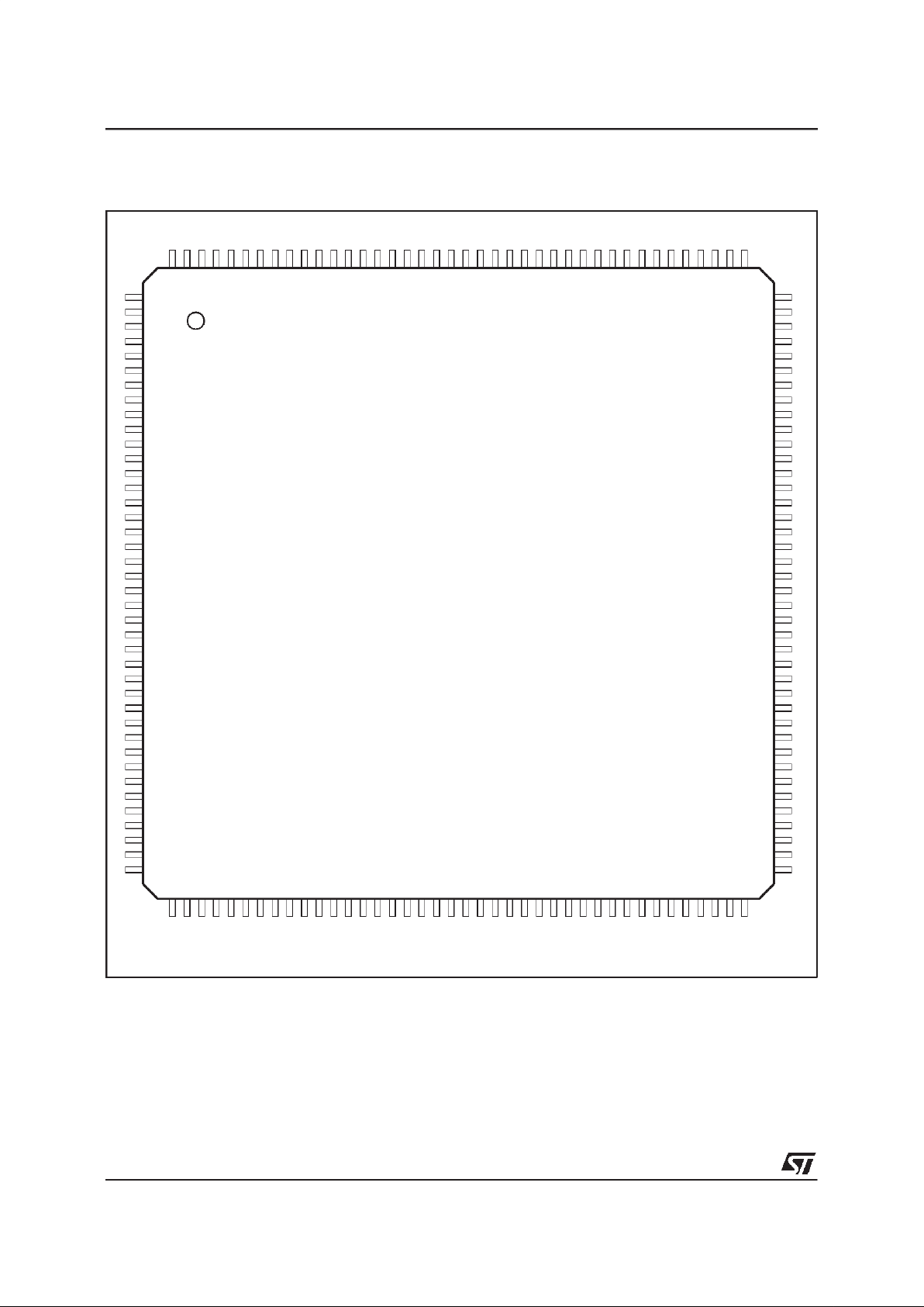
I - PIN INFORMATION
I.1 - Pin Connections
STLC5465B
8/101
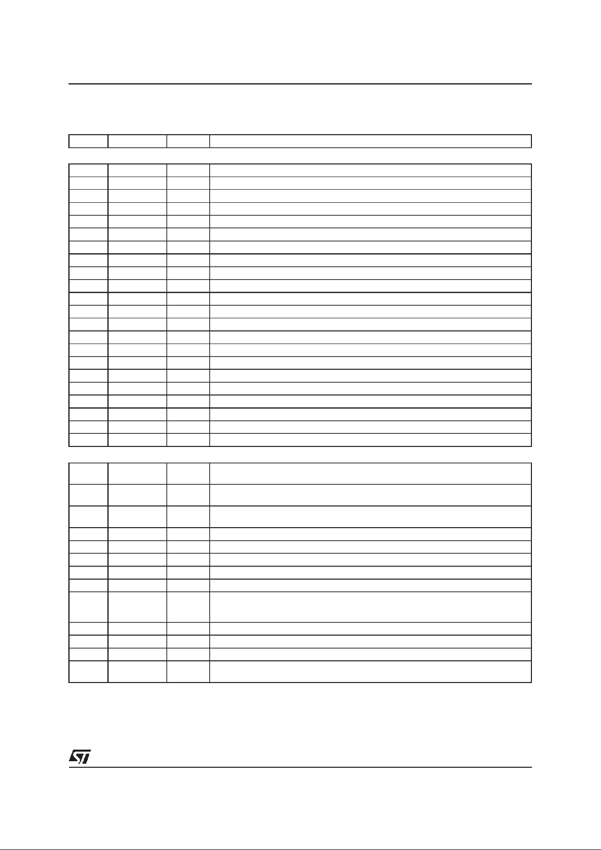
I.2 - Pin Description
Pin N° Symbol Type Function
POWER PINS (all thepower and ground pins must beconnected)
14 V
DD1
Power DC supply
15 V
SS1
Ground DC ground
29 V
DD2
Power DC supply
30 V
SS2
Ground DC ground
45 V
DD3
Power DC supply
46 V
SS3
Ground DC ground
61 V
DD4
Power DC supply
62 V
SS4
Ground DC ground
73 V
DD5
Power DC supply
74 V
SS5
Ground DC ground
89 V
DD6
Power DC supply
90 V
SS6
Ground DC ground
107 V
DD7
Power DC supply
108 V
SS7
Ground DC ground
121 V
DD8
Power DC supply
122 V
SS8
Ground DC ground
133 V
DD9
Power DC supply
134 V
SS9
Ground DC ground
145 V
DD10
Power DC supply
146 V
SS10
Ground DC ground
158 V
DD11
Power DC supply
159 V
SS11
Ground DC ground (Total 22)
CLOCKS
2 XTAL1 I Crystal 1. A clock pulse at f
Min.
= 32000kHz can be applied to this input (or one pin
of two crystal pins) with : -50.10
-6
<∆f < +50.10-6.
3 XTAL2 O Crystal 2. If the internal crystal oscillator is used, the second crystal pin is applied
to this output.
7 VCXO IN I3 VCXO input signal. This signal is compared to clock A(or B) selected inside the
Multi-HDLC
.
8 VCXO OUT O4 VCXO errorsignal. This pin delivers the result of the comparison.
10 CLOCKA I3 Input ClockA (4096kHz or 8192kHz)
11 CLOCKB I3 Input ClockB (4096kHz or 8192kHz)
12 FRAMEA I3 Clock A at 8kHz
13 FRAMEB I3 Clock B at 8kHz
9 DCLK O8 Data Clock issued from Input Clock A (or B). This clock is delivered by the circuit
at 4096kHz(or2048kHz). DOUT0/7 aretransmittedonthe risingedge of thissignal.
DIN0/7 are sampled on the falling edge of this signal.
17 FSCG O8 Frame synchronizationfor GCI at 8kHz. This clock is issuedfrom FRAME A(or B).
18 FSCV* O8 Frame synchronization for V Star at 8kHz
16 FS I3 Frame synchronization.This signal synchronizes DIN0/7 and DOUT0/7.
19 PSS O8 Programmable synchronization Signal. The PS bit of connection memory is read
in real time.
Type : I1 = Input TTL ; I2 = I1 + Pull-up ; I3 = I1+ Hysteresis ; I4 = I3 + Pull-up;
O4 = Output CMOS 4mA ; O4T = O4 + Tristate ; O8 = Output CMOS 8mA, ”1” and ”0” at Low Impedance ;
O8D = Output CMOS 8mA, Open Drain ; O8DT = Output CMOS 8mA, Open Drain or Tristate;
O8T = Output CMOS 8mA, Tristate
I1 and I3 must be connected toVDD and VSS if not used
I - PIN INFORMATION (continued)
STLC5465B
9/101
I.2 - Pin Description(continued)
Pin N° Symbol Type Function
TIMEDIVISION MULTIPLEXES (TDM)
20 DIN0 I1 TDM0 Data Input 0
21 DIN1 I1 TDM1 Data Input 1
22 DIN2 I1 TDM2 Data Input 2
23 DIN3 I1 TDM3 Data Input 3
24 DIN4 I1 TDM4 Data Input 4
25 DIN5 I1 TDM5 Data Input 5
26 DIN6 I1 TDM6 Data Input 6
27 DIN7 I1 TDM7 Data Input 7
28 DIN8 I1 TDM8 Data Input 8
31 DOUT0 O8DT TDM0 Data Output 0
32 DOUT1 O8DT TDM1 Data Output 1
33 DOUT2 O8DT TDM2 Data Output 2
34 DOUT3 O8DT TDM3 Data Output 3
35 DOUT4 O8DT TDM4 Data Output 4
36 DOUT5 O8DT TDM5 Data Output 5
37 DOUT6 O8DT TDM6 Data Output 6
38 DOUT7 O8DT TDM7 Data Output 7
39 NDIS I1 DOUT 0/7 Not Disable. When this pin is at 0V, the Data Output 0/7 are at high
impedance. Wired at VDD ifnot used.
5 CB O8D Contention Bus for CSMA/CR
6 EC I1 Echo
BOUDARY SCAN
40 NTRST I4 Reset for boundary scan
41 TMS I2 Mode Selection for boundary scan
42 TDI I2 Input Data for boundaryscan
43 TDO O4 Output Datafor boundary scan
44 TCK I2 Clock for boundary scan
MICROPROCESSOR INTERFACE
58 MOD0 I1 1 1 0 0 1 1 0
59 MOD1 I1 1 1 0 0 0 0 1
60 MOD2 I1 0 1 1 0 0 1 1
80C188 80C186 68000 68020 ST9 ST10m ST10Nm
1 NRESET I3 Circuit Reset
47 NCS0 I3 Chip Select0 : internal registers are selected
48 NCS1 I3 Chip Select1 : external memory is selected
49 INT0 O4 Interrupt generated by HDLC, RxC/I or RxMON. Active high.
50 INT1 O4 Interrupt1.This pin goes to 5V when the selected clock A (or B) has disappeared ;
250µs after reset this pin goesto 5V also if clock A is not present.
4 WDO O4 Watch Dog Output.This pingoes to5V during1ms whenthe microprocessorhasnot
reset the Watch Dog during the programmable time.
Type : I1 = Input TTL ; I2 = I1 + Pull-up ; I3 = I1+ Hysteresis ; I4 = I3 + Pull-up;
O4 = Output CMOS 4mA ; O4T = O4 + Tristate ; O8 = Output CMOS 8mA, ”1” and ”0” at Low Impedance ;
O8D = Output CMOS 8mA, Open Drain ; O8DT = Output CMOS 8mA, Open Drain or Tristate;
O8T = Output CMOS 8mA, Tristate
I - PIN INFORMATION (continued)
STLC5465B
10/101
I.2 - Pin Description(continued)
Pin N° Symbol Type Function
MICROPROCESSOR INTERFACE (continued)
51 SIZE0/NLDS I3 Transfer Size0 (68020)/Lower Data Strobe (68000)
52 SIZE1/NBHE/NUDS I3 Transfer Size1 (68020)/Bus High Enable (Intel) / Upper Data Strobe (68000)
53 NDSACK0/NDTACK O8T DataStrobe, Acknowledge and Size0 (68020)/Data Transfer Acknowledge
(68000)
54 NDSACK1/READY O8T Data Strobe, Acknowledge and Size0 (68020)/Data Transfer Acknowledge
(Intel)
55 NAS/ALE I3 Address Strobe(Motorola) / Addresss Latch Enable(Intel)
56 R/W / NWR I3 Read/Write (Motorola / Write(Intel)
57 NDS/NRD I3 DataStrobe (Motorola 68020); at Vdd for 68000/Read Data (Intel)
63 A0/AD0 I/O Address bit 0(Motorola 68020);at Vdd for 68000 / Address/Data bit 0 (Intel)
64 A1/AD1 I/O Address bit 1(Motorola) / Address/Data bit1 (Intel)
65 A2/AD2 I/O Address bit 2(Motorola) / Address/Data bit2 (Intel)
66 A3/AD3 I/O Address bit 3(Motorola) / Address/Data bit3 (Intel)
67 A4/AD4 I/O Address bit 4(Motorola) / Address/Data bit4 (Intel)
68 A5/AD5 I/O Address bit 5(Motorola) / Address/Data bit5 (Intel)
69 A6/AD6 I/O Address bit 6(Motorola) / Address/Data bit6 (Intel)
70 A7/AD7 I/O Address bit 7(Motorola) / Address/Data bit7 (Intel)
71 A8/AD8 I/O Address bit 8(Motorola) / Address/Data bit8 (Intel)
72 A9/AD9 I/O Address bit 9(Motorola) / Address/Data bit9 (Intel)
75 A10/AD10 I/O Address bit 10 (Motorola) / Address/Data bit 10 (Intel)
76 A11/AD11 I/O Address bit 11 (Motorola) / Address/Data bit 11 (Intel)
77 A12/AD12 I/O Address bit 12 (Motorola) / Address/Data bit 12 (Intel)
78 A13/AD13 I/O Address bit 13 (Motorola) / Address/Data bit 13 (Intel)
79 A14/AD14 I/O Address bit14 (Motorola) / Address/Data bit 14 (Intel)
80 A15/AD15 I/O Address bit15 (Motorola) / Address/Data bit 15 (Intel)
81 A16 I1 Address bit16 (Motorola) / Address bit 16 (Intel)
82 A17 I1 Address bit17 (Motorola) / Address bit 17 (Intel)
83 A18 I1 Address bit18 (Motorola) / Address bit 18 (Intel)
84 A19 I1 Address bit19 (Motorola) / Address bit 19 (Intel)
85 A20/ADM15 I/O Address bit 20 from µP (input) / Address bit 15 for SRAM (output)
86 A21/ADM16 I/O Address bit 21 from µP (input) / Address bit 16 for SRAM (output)
87 A22/ADM17 I/O Address bit 22 from µP (input) / Address bit 17 for SRAM (output)
88 A23/ADM18 I/O Address bit 23 from µP (input) / Address bit 18 for SRAM (output)
91 DO I/O Databit 0 for µP if not multiplexed (see Note 1).
92 D1 I/O Databit 1 for µP if not multiplexed
93 D2 I/O Databit 2 for µP if not multiplexed
94 D3 I/O Databit 3 for µP if not multiplexed
95 D4 I/O Databit 4 for µP if not multiplexed
96 D5 I/O Databit 5 forµP if not multiplexed
97 D6 I/O Databit 6 for µP if not multiplexed
98 D7 I/O Databit 7 for µP if not multiplexed
99 D8 I/O Databit 8 forµP if not multiplexed
Type : I1 = Input TTL ; I2 = I1 + Pull-up ; I3 = I1+ Hysteresis ; I4 = I3 + Pull-up;
O4 = Output CMOS 4mA ; O4T = O4 + Tristate ; O8 = Output CMOS 8mA, ”1” and ”0” at Low Impedance ;
O8D = Output CMOS 8mA, Open Drain ; O8DT = Output CMOS 8mA, Open Drain or Tristate;
O8T = Output CMOS 8mA, Tristate
I - PIN INFORMATION (continued)
STLC5465B
11/101
I.2 - Pin Description(continued)
Pin N° Symbol Type Function
MICROPROCESSOR INTERFACE (continued)
100 D9 I/O Data bit 9 for µP if not multiplexed
101 D10 I/O Data bit 10 for µP if not multiplexed
102 D11 I/O Data bit 11 forµP if not multiplexed
103 D12 I/O Data bit 12 for µP if not multiplexed
104 D13 I/O Data bit 13 for µP if not multiplexed
105 D14 I/O Data bit 14 forµP if not multiplexed
106 D15 I/O Data bit 15 for µP if not multiplexed
MEMORY INTERFACE
109 TRI I3 Token Ring Input (foruse
Multi-HDLC
s in cascade)
110 TRO O4 Token Ring Output (for use
Multi-HDLC
s in cascade)
111 NWE O4T Write Enable for memory circuits
112 NOE O4T Control Output Enable for memory circuits
113 NRAS0/NCE0 O4T Row Address Strobe Bank 0 / Chip Enable 0 for SRAM
114 NCAS0/NCE1 O4T Column Address Strobe Bank 0 / Chip Enable1 for SRAM
115 NRAS1/NCE2 O4T Row Address Strobe Bank 1 / Chip Enable 2 for SRAM
116 NCAS1/NCE3 O4T Column Address Strobe Bank 1 / Chip Enable 3 for SRAM
117 NRAS2/NCE4 O4T Row Address Strobe Bank 2 / Chip Enable 4 for SRAM
118 NCE5 O4T Chip Enable 5 for SRAM
119 NRAS3/NCE6 O4T Row Address Strobe Bank 3 / Chip Enable 6 for SRAM
120 NCE7 O4T Chip Enable 7 for SRAM
123 ADM0 O8T Address bit 0 for SRAM and DRAM
124 ADM1 O8T Address bit 1 for SRAM and DRAM
125 ADM2 O8T Address bit 2 for SRAM and DRAM
126 ADM3 O8T Address bit 3 for SRAM and DRAM
127 ADM4 O8T Address bit 4 for SRAM and DRAM
128 ADM5 O8T Address bit 5 for SRAM and DRAM
129 ADM6 O8T Address bit 6 for SRAM and DRAM
130 ADM7 O8T Address bit 7 for SRAM and DRAM
131 ADM8 O8T Address bit 8 for SRAM and DRAM
132 ADM9 O8T Address bit 9 for SRAM and DRAM
135 ADM10 O8T Address bit 10 for SRAM and DRAM
136 ADM11 O8T Address bit 11 for SRAM only
137 ADM12 O8T Address bit 12 for SRAM only
138 ADM13 O8T Address bit 13 for SRAM only
139 ADM14 O8T Address bit 14 for SRAM only
Type : I1 = Input TTL ; I2 = I1 + Pull-up ; I3 = I1+ Hysteresis ; I4 = I3 + Pull-up;
O4 = Output CMOS 4mA ; O4T = O4 + Tristate ; O8 = Output CMOS 8mA, ”1” and ”0” at Low Impedance ;
O8D = Output CMOS 8mA, Open Drain ; O8DT = Output CMOS 8mA, Open Drain or Tristate;
O8T = Output CMOS 8mA, Tristate
I - PIN INFORMATION (continued)
STLC5465B
12/101

I.2 - Pin Description(continued)
Pin N° Symbol Type Function
MEMORY INTERFACE (continued)
140 DM0 I/O Memory Data bit 0
141 DM1 I/O Memory Data bit 1
142 DM2 I/O Memory Data bit 2
143 DM3 I/O Memory Data bit 3
144 DM4 I/O Memory Data bit 4
147 DM5 I/O Memory Data bit 5
148 DM6 I/O Memory Data bit 6
149 DM7 I/O Memory Data bit 7
150 DM8 I/O Memory Data bit 8
151 DM9 I/O Memory Data bit 9
152 DM10 I/O Memory Data bit 10
153 DM11 I/O Memory Data bit 11
154 DM12 I/O Memory Data bit 12
155 DM13 I/O Memory Data bit 13
156 DM14 I/O Memory Data bit 14
157 DM15 I/O Memory Data bit 15
160 NTEST I2 Test Control. When this pin is at 0V each output is high impedance except XTAL2 Pin.
Type : I1 = Input TTL ; I2 = I1 + Pull-up ; I3 = I1+ Hysteresis ; I4 = I3 + Pull-up;
O4 = Output CMOS 4mA ; O4T = O4 + Tristate ; O8 = Output CMOS 8mA, ”1” and ”0” at Low Impedance ;
O8D = Output CMOS 8mA, Open Drain ; O8DT = Output CMOS 8mA, Open Drain or Tristate;
O8T = Output CMOS 8mA, Tristate
Note : D0/15 input/outputpins must be connected to one single external pull up resistor if not used.
I.3 - Pin Definition
I.3.1- Input Pin Definition
I1 : Input 1 TTL
I2 : Input 2 TTL+ pull-up
I3 : Input 3 TTL+ hysteresis
I4 : Input 4 TTL+hysteresis+pull-up
I.3.2- OutputPin Definition
O4 : OutputCMOS4mA
O4T : OutputCMOS4mA, Tristate
O8 : OutputCMOS8mA
O8T : OutputCMOS8mA,Tristate
O8D : Output CMOS 8mA,Open Drain
O8DT : OutputCMOS 8mA,OpenDrain or Tristate(Programmable pin)
Moreover, each output is high impedance when the NTEST Pin is at 0 volt except XTAL2 Pin which is a
CMOSoutput.
I.3.3- Input/Output Pin Definition
I/O: Input TTL/ OutputCMOS 8mA.
N.B. XTAL1 : this input is CMOS.
XTAL2 : NTESTpin at 0 has no effecton this pin.
I - PIN INFORMATION (continued)
STLC5465B
13/101
Pseudo
Random
Sequence
Generator
7
COUNTER
XTAL
WATCHDOG
µP
INTERFACE
CLOCK
SELECTION
RAM
INTERFACE
8
2
3284
27
26
VCX OUT
XTAL1
XTAL2
DIN8
WDO
GCI1
GCI0
25 24 23 22 21 20
DIN5
DIN4
DIN3
DIN2
DIN1
DIN0
0123456
7
0123456
7
D7
Pseudo
Random
Sequence
Analyser
39 31 32 33 34
NDIS
DOUT0
DOUT1
DOUT2
DOUT3
SWITCHINGMATRIX
n x 64 kb/s
35
GCI0
36
DOUT4
DOUT5
37
DOUT6
GCI1
38
DOUT7
12
FRAMEA
10
CLOCKA
13
FRAME B
11
CLOCKB
18
17
9
FSCV*
FSCG
DCLK
To
Internal
Circuit
16 FS
5CB
TIME SLOT ASSIGNERFOR MULTIHDLC
GCI CHANNELDEFINITION
V10
32 Rx HDLC
with Adress
Recognition
32 Rx DMAC
16 Rx
C/I
16 Rx
MON
16 Tx
C/I
16 Tx
MON
6EC
32 Tx HDLC
with CSMACR
for Content. Bus
32 Tx DMAC
µPBus
INTERRUPT
CONTROLLER
Rx
C/I
Rx
MON
Rx
DMAC DMAC
Tx
RAM
Bus
49 INT0
50 INT1
InternalBus
BUS ARBITRATION
STLC5465
V10
VCX IN
DIN7
DIN6
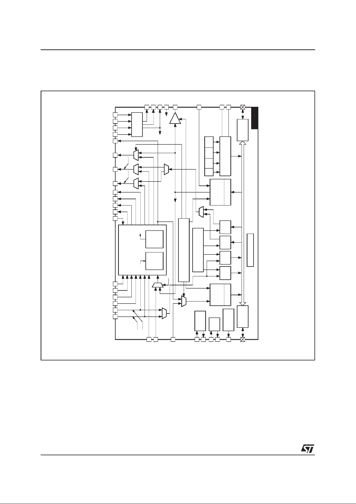
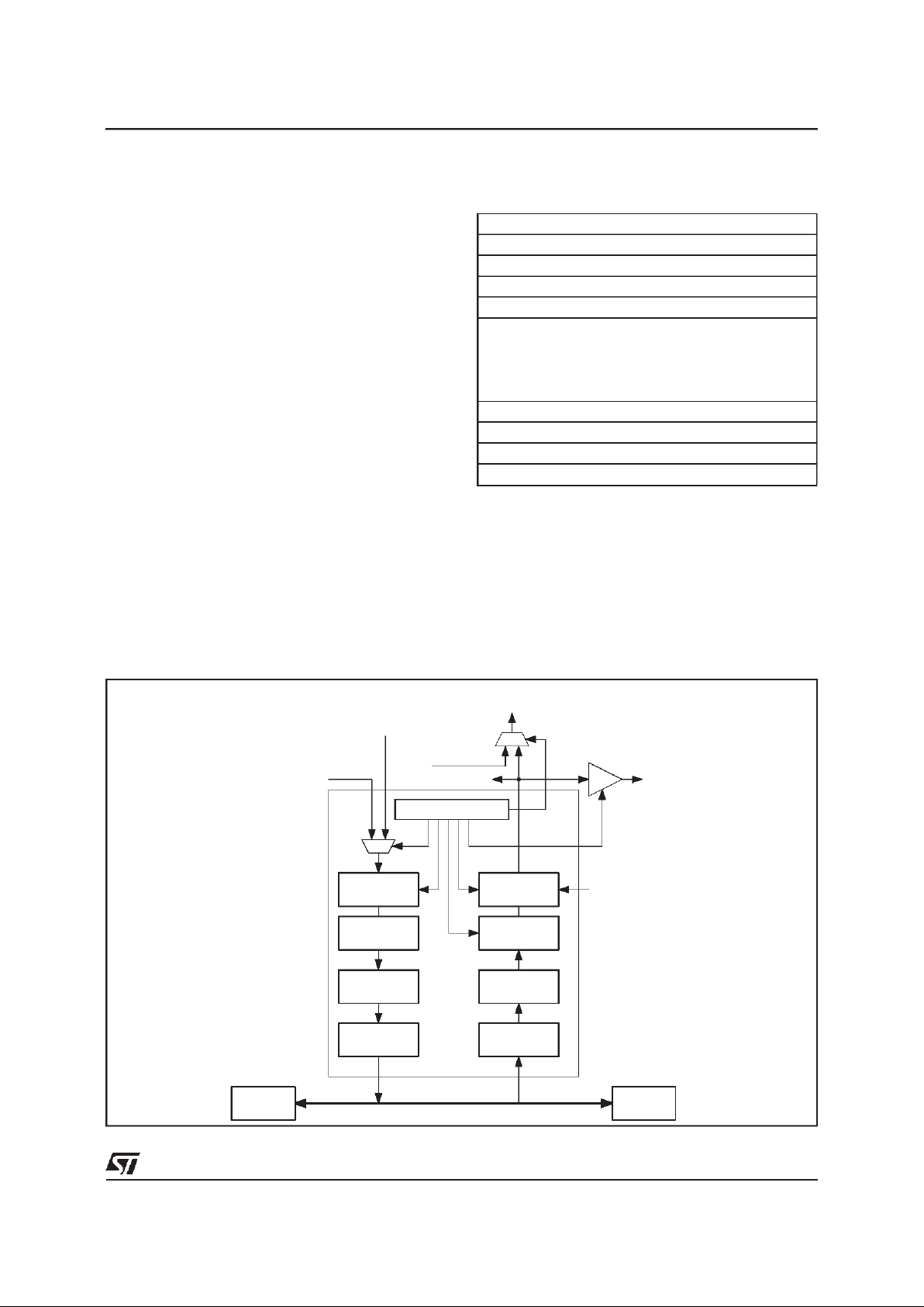
Figure1 : GeneralBlockDiagram
II - BLOCK DIAGRAM
Thetop levelfunctionalitiesof
Multi-HDLC
appearon the general block diagram.
Thereare :
- The switching matrix,
- The time slot assigner,
- The 32 HDLC transmitterswith associated DMA
controllers,
- The 32 HDLC receivers with associated DMA
controllers,
- The 16 Command/Indicateand Monitor Channel
transmitters belonging to two General Component Interfaces(GCI),
- The 16 Command/Indicateand Monitor Channel
receivers belonging to two General Component
Interfaces(GCI),
- The memory interface,
- The microprocessor interface,
- The bus arbitration,
- The clock selection and time synchronization
function,
- The interrupt controller,
- The watchdog,
- The boundaryscan.
STLC5465B
14/101

III - FUNCTIONALDESCRIPTION
III.1- The SwitchingMatrix N x 64 KBits/S
III.1.1 - FunctionDescription
The matrix performs a non-blockingswitch of 256
time slots from 8 Input Time Division Multiplex
(TDM) at 2 Mbit/s to 8 output TimeDivision Multiplex.ATDM is composedof 32 TimeSlots (TS) at
64 kbit/s. The matrix is designed to switch a 64
kbit/s channel (Variable delay mode) or an hyperchannel of data (Sequence integrity mode). So, it
will both provide minimum throughput switching
delayfor voiceapplicationsandtimeslotsequence
integrity for data applications on a per channel
basis.
The requirements of the Sequence Integrity(n*64
kbit/s)mode are the following:
Allthe timeslotsofagiveninputframe mustbe put
out during a same output frame.
The time slots of an hyperchannel (concatenation
of TS in the same TDM) are not crossed together
at output in different frames.
In variable delay mode, the time slot is put out as
soon as possible. (The delay is two or three time
slots minimum between input and output).
For test facilities, any time slot of an Output TDM
(OTDM) can be internally looped back into the
sameInputTDM number(ITDM)at thesametime
slotnumber.
A Pseudo Random Sequence Generator and a
Pseudo Random Sequence Analyzer are implemented in the matrix.They allow the generationa
sequence on a channel or on a hyperchannel, to
analyse it and verify its integrity after several
switching in the matrix or some passing of the
sequenceacrossdifferentboards.
The Frame Signal (FS) synchronises ITDM and
OTDMbut a programmabledelayor advance can
beintroducedseparatelyon eachITDMand OTDM
(a half bit time, a bit time or two bit times).
An additional pin (PSS) permits the generationof
a programmablesignal composed of 256 bitsper
frameat a bit rate of 2048kbit/s.
An external pin (NDIS) asserts a high impedance
on all the TDM outputs of the matrix when active
(duringthe initializationof theboard for example).
III.1.2 - Architectureof the Matrix
The matrix is essentially composed of bufferdata
memoriesand a connection memory.
Thereceivedserialdataisfirst convertedto parallel
byaserialtoparallelconverterandstoredconsecutively in a 256 position Buffer Data Memory (see
Figure 2 on Page 16).
To satisfy the SequenceIntegrity (n*64 kbit/s) requirements,the data memory is built with an even
memory, an odd memory and an output memory.
Twoconsecutiveframes are storedalternativelyin
theoddandevenmemory.Duringthetimeaninput
frame is stored,theone previouslystoredis transferred into the output memory according to the
connectionmemoryswitchingorders.Aframelater,
the outputmemoryis readand datais convertedto
serial and transferredto the output TDM.
III.1.3 - Connection Function
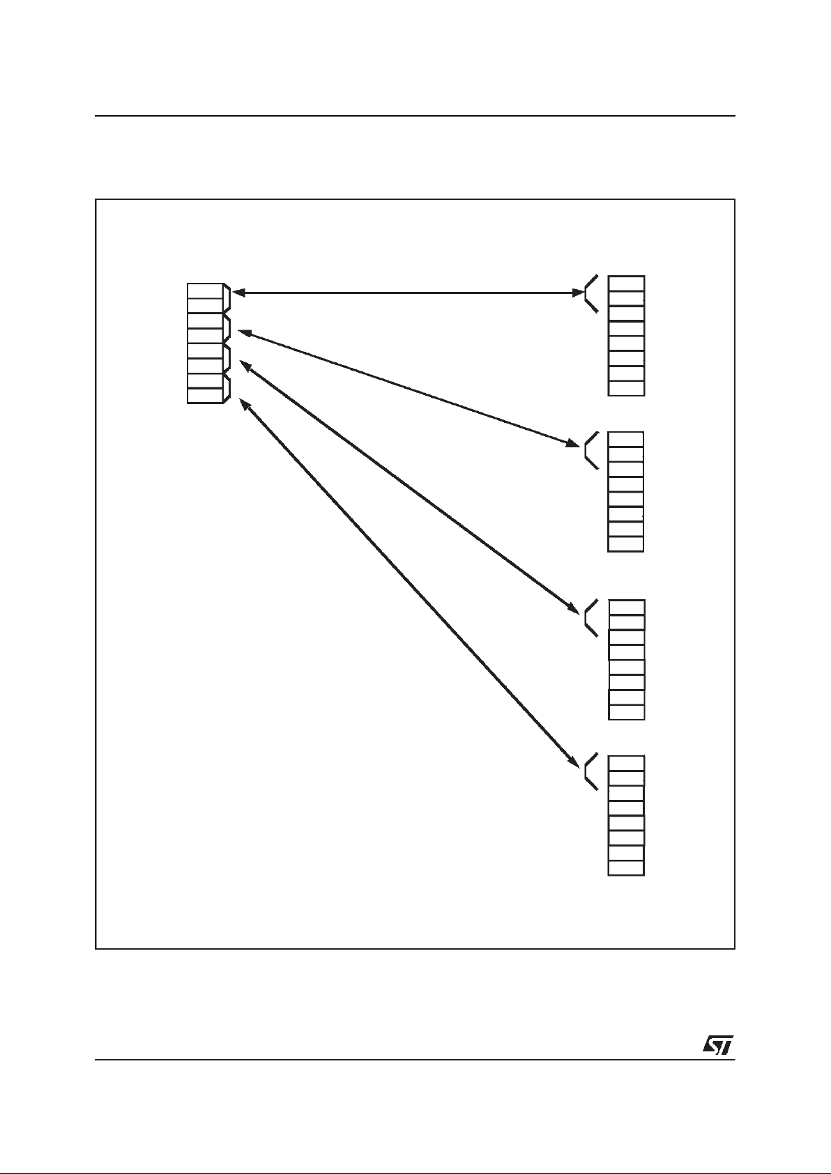
Twotypes of connectionsare offered:
- unidirectionalconnectionand
- bidirectionalconnection.
Anunidirectionalconnectionmakesonly theswitch
ofaninputtimeslotthroughanoutputone whereas
abidirectionalconnectionestablishesthelinkin the
other directiontoo.So a doubleconnectioncan be
achieved by a single command (see Figure 3 on
Page 17).
III.1.4 - LoopBackFunction
Any time slot of an Output TDM can be internally
looped back on the time slot which has the same
TDM number and the same TS number
(OTDMi,TSj) ----> (ITDMi, TSj).
In the case of a bidirectional connection,only the
one specifiedby the microprocessoris concerned
by the loop back (see Figure 4 on Page 17).
STLC5465B
15/101
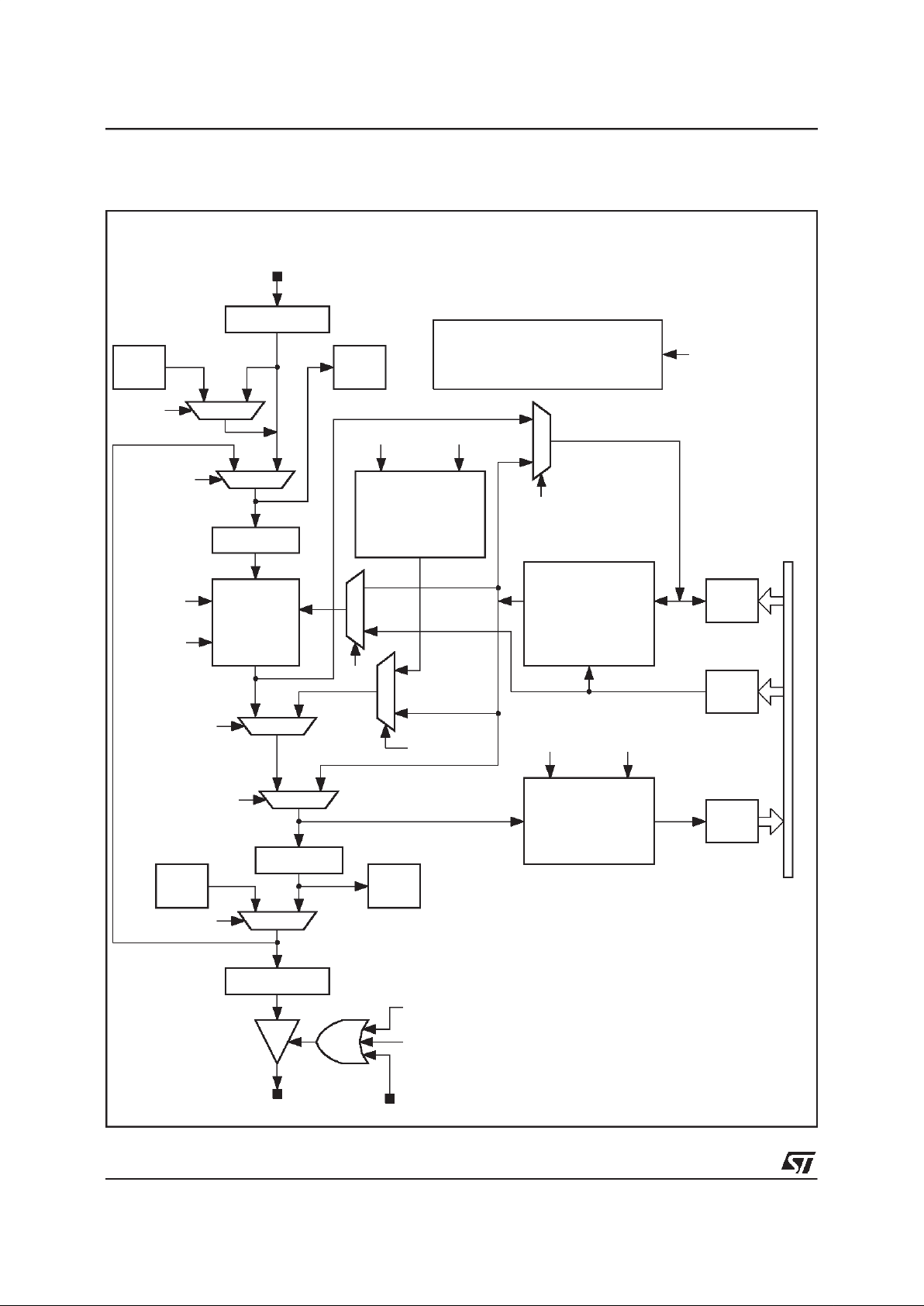
From SMCR Register
CM
(whenRead)
LOOP
DATA
MEMORIES
64kb/s and
n x 64kb/s
CONNECTION
MEMORY
SequenceIntegrity,
LOOP, PRSA,PRSG,
INS, OTSV
Tx
HDLC
Rx
GCI
S/P
IMTD
Sequence
Integrity
INS
1
1
A
1
CM
1
PRSG
PSEUDORANDOM
SEQUENCE
GENERATOR
211-1
Rec. O.152
PRSG
SGV
PSEUDORANDOM
SEQUENCE
ANALYZER
211-1
Rec. O.152
PRSA
SAV
GCIR
BIT SYNCHRO
Tx
GCI
ME
P/S
Rx
HDLC
D4/5
D7
D0/7
1
1
D
D
D
D
A
1
CMDR
Data
Register
CMAR
Address
Register
SFCRR
SequenceFault
CounterRegister
HDLCM 1
D7 DDIINN’0/7
7
D4/5
BIT SYNCHRO
DIN 0/7
DOUT 0/7
Internal
Bus
From OMCRRegister
OMV(per multiplex)
From Connection Memory
OTSV(perchannel)
From N DIS PIN
(for all multiplexes)
PRSG :
Pseudo RandomSequenceGenerator
PRSA :
PseudoRandomSequenceAnalyzer
OTSV :
OutputTime Slot Validated
INS :
Insert
ME
: gMessa e Enable
IMTD : IncreasedMin ThroughtputDelay
SGV : SequenceGenerator Validated
SAV :
SequenceAnalyzer Validated
CM : Connection Memory(from CMARRegister)
OR
Figure2 : Switching Matrix Data Path
III - FUNCTIONALDESCRIPTION (continued)
STLC5465B
16/101
OTSy, OTDMq
DATA
MEMORY
n x 64kb/s
DATA
MEMORY
n x 64kb/s
DOWN STREAM
ITSy, ITDMq
UP STREAM
ITSx,ITDMp
DOWN STREAM
OTSx, OTDMp
UP STREAM
Bidirectional Connection
OTSy, OTDMq
DATA
MEMORY
n x 64kb/s
DOWN STREAM
ITSx,ITDMp
DOWN STREAM
Unidirectional Connection
p, q = 0 to 7
x, y= 0 to 31
5464-04.EPS
Figure3 : Unidirectionaland BidirectionalConnections
OTSy, OTDMq
DATA
MEMORY
n x 64kb/s
DATA
MEMORY
n x 64kb/s
DOWN STREAM
ITSy, ITDMq
UP STREAM
ITSx,ITDMp
DOWN STREAM
OTSx, OTDMp
UP STREAM
OTSV
Loop
Loopback per channel relevant if bidirectional connection has been done.
p, q = 0 to 7
x, y = 0 to 31
5464-05.EPS
Figure4 : LoopBack
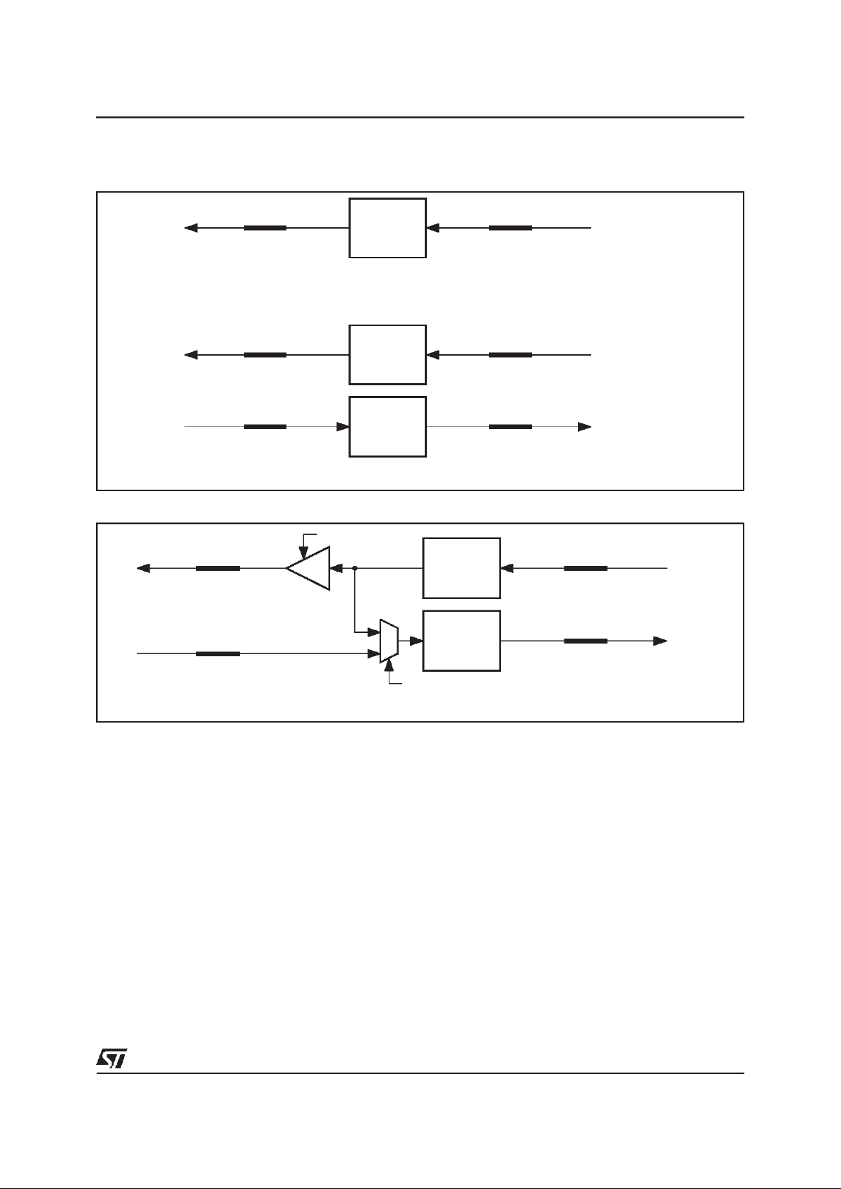
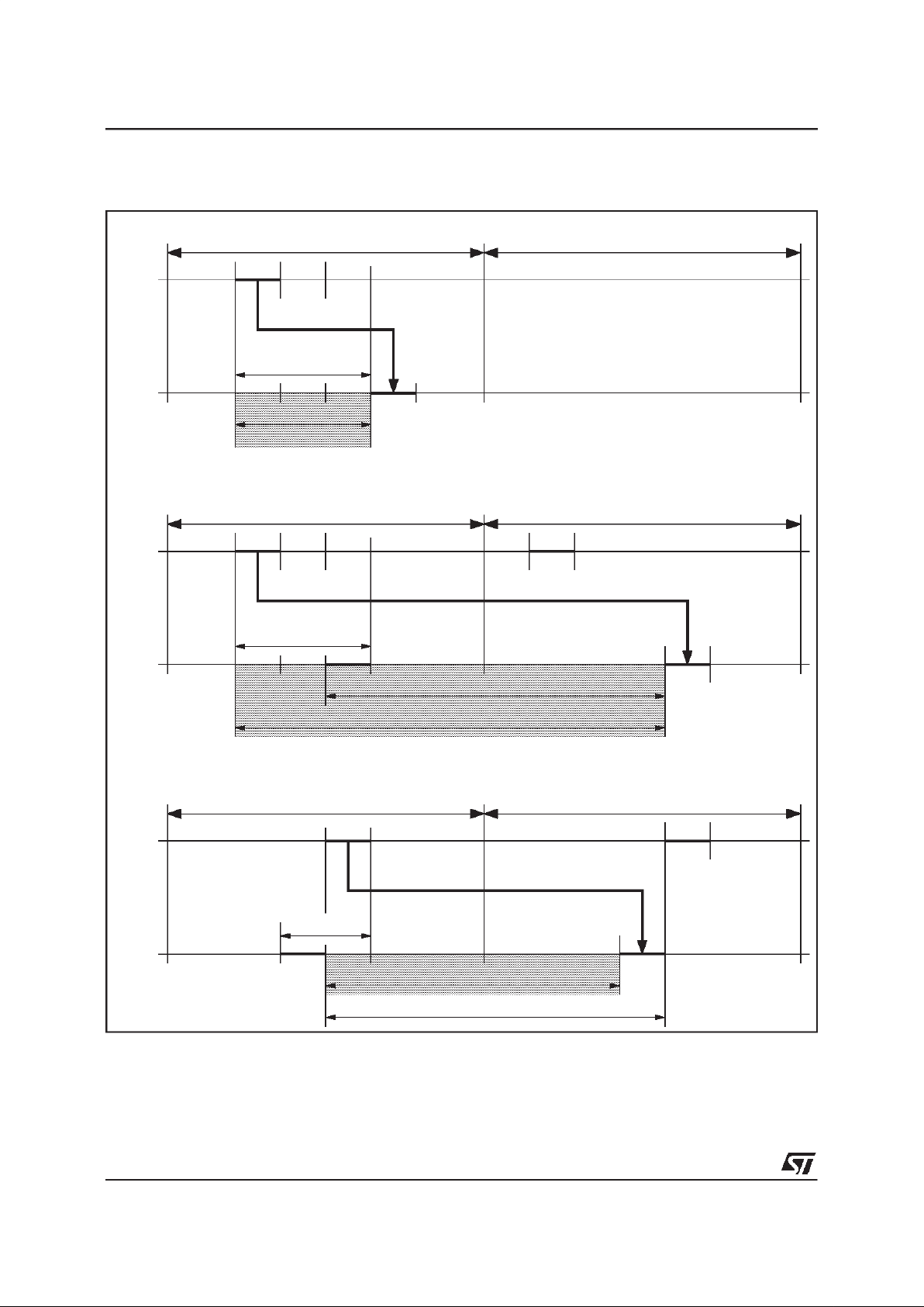
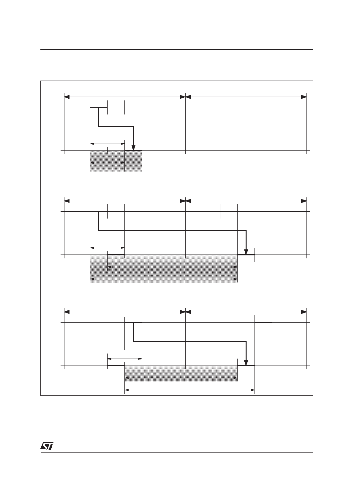
III - FUNCTIONALDESCRIPTION (continued)
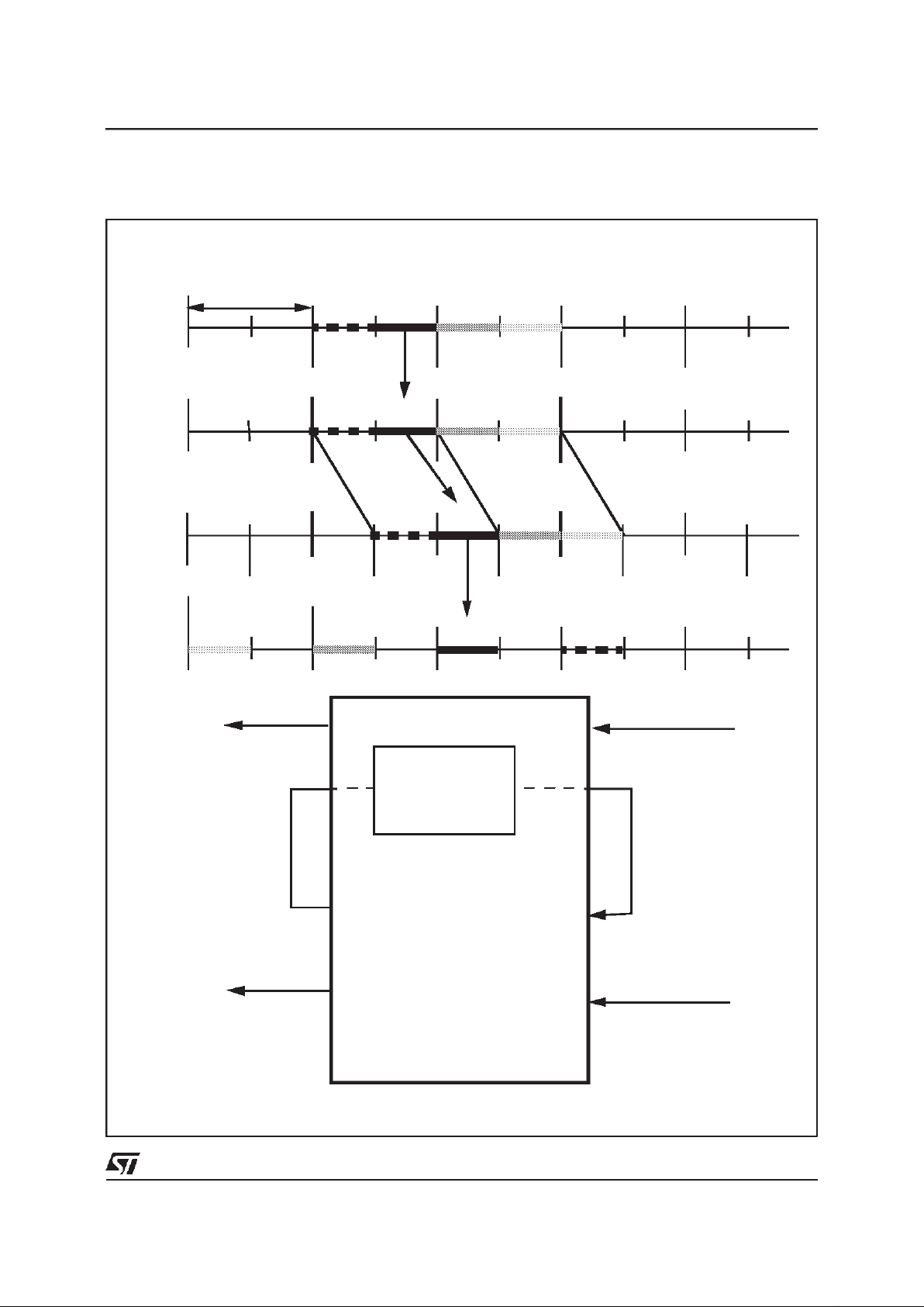
III.1.5 - Delay through the Matrix
III.1.5.1- VariableDelay Mode
In the variable delay mode, the delay through the
matrixdependson therelativepositionsof theinput
and output time slots in the frame.
So,some limitsare fixed :
- the maximumdelay isa frame+ 2 time slots,
- the minimum delay is programmable.
Three time slots if IMTD= 1, in this case n = 2 in
the fo rmula he reafter or two time slots if
IMTD = 0, in this case n = 1 in the sameformula
(see Paragraph ”Switching Matrix Configuration
Reg SMCR(0C)H” on Page 64).
Allthe possibilitiescanbe ranked in three cases :
a) If OTSy > ITSx + n then thevariabledelay is :
OTSy- ITSx Timeslots
b) IfITSx< OTSy< ITSx+nthenthevariabledelay
is :
OTSy - ITSx + 32 Timeslots
c) OTSy< ITSxthen the variable delay is :
32 - (ITSx- OTSy)Time slots.
N.B. Ruleb) and rule c) are identical.
For n = 1 and n = 2, seeFigure 5 on Page 18.
III.1.5.2- SequenceIntegrity Mode
In the sequenceintegrity mode (SI = 1, bitlocated
in theConnectionMemory),theinputtimeslotsare
putout2frameslater(fig.6-page19).Inthiscase,
the delay is definedby a single expression:
ConstantDelay = (32 - ITSx)+ 32 + OTSy
So, the delay in sequence integrity mode varies
from 33 to 95 timeslots.
STLC5465B
17/101
Frame n Frame n + 1
ITS0 ITS31 ITS0 ITS31
OTS0 OTS31
ITSx ITSx+1 ITSx+2
OTSy
y>x+2
Variable De lay
(OTSy - ITSx)
Inpu t
Frame
Output
Frame
1) Cas e : If OTSy > ITS x + 2, then Variable Delay is : OTS y - ITSx TimeSlots
Frame n Frame n + 1
ITS0 ITS31 ITS0 ITS31
OTS0 OTS31
ITSx ITSx+1 ITSx+2
OTSy
x≤y≤x+2
32 TimeS lots
Variable De lay : OTS y - ITSx + 32 TimeSlots
Inpu t
Frame
Output
Frame
2) Cas e : If ITSx≤OTSy≤ITSx + 2, the n Variable De lay is : OTSy - ITSx + 32 TimeSlots
ITSx
OTSy
Frame n Frame n + 1
ITS0 ITS31 ITS0 ITS31
OTS0 OTS31
ITSx
OTSy
y<x
32 Tim eSlots
Variable Delay : 32 - (ITSx - OTSy) TimeS lots
Inpu t
Frame
Output
Frame
3) Cas e : If OTSy < ITS x, the n Variable De lay is : 32 - (ITSx - OTSy) TimeSlots
ITSx
OTSy
5464-06.EPS
Figure5 : VariableDelay through the matrixwith ITDM = 1
III - FUNCTIONALDESCRIPTION (continued)
STLC5465B
18/101
Frame n Frame n + 1
ITS0 ITS31 ITS0 ITS31
OTS0 OTS31
ITSx ITSx+1 ITSx+2
OTSy
y>x+1
Variable Delay
(OTSy - ITSx)
Input
Frame
Output
Frame
1) Case : If OTSy > ITSx + 1, then Variable Delay is : OTSy - ITSx TimeSlots
Frame n Frame n + 1
ITS0 ITS31 ITS0 ITS31
OTS0 OTS31
ITSx ITSx+1 ITSx+2
OTSy
x
≤ y ≤ x+1
32 TimeSlots
Variable Delay : OTSy - ITSx + 32 TimeSlots
Input
Frame
Output
Frame
2) Case : If ITSx ≤ OTSy ≤ ITSx + 1, thenVariable Delay is : OTSy - ITSx + 32 TimeSlots
ITSx
OTSy
Frame n Frame n + 1
ITS0 ITS31 ITS0 ITS31
OTS0 OTS31
ITSx
OTSy
y<x
32 TimeSlots
Variable Delay : 32 - (ITSx - OTSy) TimeSlots
Input
Frame
Output
Frame
3) Case : If OTSy < ITSx, then Variable Delay is : 32 - (ITSx - OTSy) TimeSlots
ITSx
OTSy
5464-07.EPS
Figure6: Variable Delay throughthe matrix with ITDM = 0
III - FUNCTIONALDESCRIPTION (continued)
STLC5465B
19/101
Cons tant Delay = (32 -ITSx) + 32 + OTSy
Framen Framen+1 Framen+2
ITS0
Min. Constant Delay = 33TS
32 Time Slots + 0 = 33
TimeSlots
Max. Constant Delay = 95 TimeSlots
32 - 0 + 32 + 31 = 95
TimeSlots
(32 - ITSx)
+32 +OTSy =Constant
Delay
ITS31 ITS0 ITS31 ITS0 ITS31
OTS0 OTS 31
1+
OTS 31
ITS :
OTS :
Input TimeSlot
Output TimeSlot
0≤x≤31
0≤y≤31
5464-08.EPS
Figure7 : Constant Delaythrough the matrixwith SI = 1
III - FUNCTIONALDESCRIPTION (continued)
STLC5465B
20/101

III.1.6 - ConnectionMemory
III.1.6.1- Description
Theconnectionmemoryis composedof256 locations addressed by the number of OTDM and TS
(8x32).
Eachlocationpermits:
- to connecteachinputtime slotto one outputtime
slot (If two or more output time slots are connected to the same inputtime slot number,there
is broadcasting).
- to selectthe variabledelaymodeorthesequence
integritymode for anytime slot.
- to loop back an output time slot. In thiscase the
contentsof aninputtime slot(ITSx,ITDMp)is the
same as the output time slot (OTSx,OTDMp).
- to output the contents of the correspondingconnection memory instead of the data which has
been storedin data memory.
- to output the sequence of the pseudo random
sequence generator on an output time slot: a
pseudo randomsequencecan be insertedin one
or severaltime slots(hyperchannel)of the same
Output TDM ; this insertion must be enabled by
the microprocessor in the configuration register
of the matrix.
- to definethe sourceof a sequenceby thepseudo
random sequence analyzer: a pseudo random
sequence can be extracted from one or several
time slots(hyperchannel)of thesame InputTDM
and routedto the analyzer;this extractioncanbe
enabled by the microprocessorin the configuration registerof the matrix (SMCR).
- to assert a high impedance level on an output
time slot (disconnection).
- to delivera programmable256-bitsequenceduring 125microsecondsontheProgrammablesynchronizationSignal pin (PSS).
III.1.6.2- Accessto ConnectionMemory
Supposingthat the Switching Matrix Configuration
Register(SMCR) has been alreadywritten by the
microprocessor, it is possibleto access to the connectionmemoryfrommicroprocessorwiththehelp
of two registers:
- ConnectionMemoryData Register (CMDR) and
- ConnectionMemoryAddressRegister(CMAR).
III.1.6.3- Accessto Data Memory
To extract the contents of the data memory it is
possible to read the datamemoryfrom microprocessor with the help of the two registers :
- ConnectionMemoryData Register (CMDR) and
- ConnectionMemoryAddressRegister(CMAR).
III.1.6.4- Switchingat 32 Kbit/s
Four TDMs can be programmed individually to
carry 64 channelsat 32 Kbit/s (onlyif theseTDMs
are at 2 Mbit/s).
Twobits(SW0/1)locatedin SMCR define the type
of channelsof two couples of TDMs.
SW0 defines TDM0 and TDM4 (GCI0) and SW1
defines TDM1 and TDM5 (GCI1). If TDM0 or/and
TDM1 carry 64 channels at 32 Kbit/s then TDM2
or/and TDM3 are not availableexternally theyare
used internally to perform the function.
Downstreamswitching at 32 kb/s on page 22.
Upstreamswitching at 32 kb/son page23.
III.1.6.5- Switchingat 16 kbit/s
TheTDM4andTDM5can beGCImultipexes.Each
GCImultipexcomprises8GCIchannels.Each GCI
channelcomprisesoneD channelat 16 Kbit/s.See
GCI channeldefinition GCI Synchro signal delivered by the Multi-HDLC on page 30.
Itispossibletoswitchthecontentsof16Dchannels
from the 16 GCI channelsto 4 timeslotsof the 256
output timeslots.
In the other direction the contents of an selected
timeslot is automaticallyswitched to 4 D channels
at 16 Kbit/s.
See Connection Memory Data Register CMDR
(0E)
H
on page 74
III - FUNCTIONALDESCRIPTION (continued)
STLC5465B
21/101

III - FUNCTIONALDESCRIPTION (continued)
dout 4 din0
dout 2 din 2
Internal
commands Switching
at 32 kb/ s
dout 5 din 1
dout 3 din 3
DIN0
din2
dout2
dout4
Internal
command
If SW0=1
DOUT4
(GCI 0)
3.9µs
a b Free c Free d Free e
abcde
ca
d b MON D C/I
dc ba
B1 B2 MON D C/I
4 bit shifting
DOUT5
DOUT4
DIN0
DIN2 notused
DIN 1
DIN3 notused
MULTI HDLC STLC546 5
SW0=1
SW1=1
4 bit shifting
(GCI 0)
(GCI 1)
DOUT2
DOUT3
D
C/I
AE
Figure8: Downstream Switching at 32kb/s
STLC5465B
22/101
III - FUNCTIONALDESCRIPTION (continued)
DOUT 0 DIN4
DOUT6 DIN6
Switching at 32 kb/s
DOUT1 DIN5
MULTI HDLC STLC 5465
DIN4
(GCI 0)
DOUT6
DIN6 =
shifted
DOUT6
DOUT0
a
Free
b
Free
c
Free
d
Free e
dc ba
B1 B2 MON D C/I
GCI1
GCI 0
From
DOUT6
d
c
b
axyz
B2 GCI 1 B1 GCI 0 B2 GCI 0 B1 GCI 1 B2 GCI1
d
c
b
a
xy
B2 GCI1 B1 GCI0 B2 GCI 0 B1 GCI1
Timeslot (3.9µs)
Internal loopback
and
4 bit shifting (2+2)
by software
Figure9: Upstream Switching at 32kb/s
STLC5465B
23/101
III - FUNCTIONALDESCRIPTION (continued)
TDM side
TSy ofany TDM can
be
programmablewith y
comprisedbetween
0 and 31
.
GCI side
D11
D12
D21
D22
D31
D32
D41
D42
TSy
D11
D12
C1
C2
C3
C4
A
E
D21
D22
C1
C2
C3
C4
A
E
D31
D32
C1
C2
C3
C4
A
E
D41
D42
C1
C2
C3
C4
A
E
n: GCIchannel
number, 0 to 1
TS 16n+15
TS 16n+11
TS 16n+7
TS 16n+3
Figure10: Upstream and DownstreamSwitchingat 16kb/s
STLC5465B
24/101
TIME S LOT ASSIGNER
32 Rx HDLC
32 ADDRESS
RECOGNITION
32 Rx FIFO’s
32 Rx DMAC 32 Rx DMAC
32 Tx FIFO’s
32 Tx HDLC
32 CSMA-CR
DIN8
Direct HDLC Input
From Output 7
of the Matrix
To Input 7 of the Matrix
From Output 6
of the Matrix
DOUT 6
Direct HDLCOutput
Conte ntion
Bus
Echo
µ
P
INTERFACE
RAM
INTERFACE
5464-09.EPS
Figure11 : HDLC and DMAControllerBlockDiagram
III - FUNCTIONALDESCRIPTION (continued)
III.2- HDLC Controller
III.2.1 - FunctionDescription
The internal HDLC controller can run up to 32
channels in a conventional HDLC mode or in a
transparent (non-HDLC) mode (configurable per
channel).
Eachchannelbitrateisprogrammablefrom 4kbit/s
to64kbit/s.All the configurationsare also possible
from 32 channels (from 4 to 64 kbit/s) to one
channelat 2 Mbit/s.
Inreception,theHDLC timeslotscan directlycome
from the input TDM DIN8 (direct HDLC Input) or
from any other TDM input after switching towards
the output 7 of the matrix (configurable per time
slot).
In transmission,the HDLC frames are senton the
output DOUT6and on the outputCB (withor without contention mechanism), or are switched towards the other TDM output via the input 7 of the
matrix(see Figure 11).
III.2.1.1- Formatof the HDLC Frame
Theformatof anHDLCframeisthesameinreceive
and transmit direction and shown here after.
III.2.1.2- Compositionof an HDLC Frame
Opening Flag
Address Field (first byte)
Address Field (second byte)
Command Field (first byte)
Command Field (second byte)
Data (first byte)
Data (optional)
Data (last byte)
FCS (first byte)
FCS (second byte)
Closing Flag
- OpeningFlag
- One or twobytes for addressrecognition(reception) andinsertion (transmission)
- Data bytes with bit stuffing
- Frame Check Sequence: CRC with polynomial
G(x) = x
16+x12+x5
+1
- Closing Flag.
STLC5465B
25/101

III.2.1.3- Descriptionand Functions of the
HDLC Bytes
- FLAG
The binarysequence01111110marksthe beginning and theend of the HDLC Frame.
Note : In reception,threepossibleflag configurations are allowed and correctlydetected:
- two normal consecutiveflags :
...0111111001111110...
- two consecutiveflags with a ”0” common:
...011111101111110...
- a global common flag : ...01111110...
this flag is the closing flag for the current frame
and the opening flag for the next frame
- ABORT
The binary sequence 1111111 marks an Abort
command.
Inreception,sevenconsecutive1’s,insidea message, are detected as an abort command and
generatesan interruptto the host.
In transmit direction, an abort is sent upon command of the micro-processor. No ending flag is
expected after the abort command.
- BIT STUFFING AND UNSTUFFING
This operation is done to avoid the confusionof
a data byte with a flag.
In transmission, if five consecutive 1’s appear in
theserialstreambeingtransmitted,a zeroisautomaticallyinserted(bit stuffing)after he fifth ”1”.
In reception,if five consecutive”1” followed by a
zero are received, the ”0” is assumed to have
been inserted and is automatically deleted (bit
unstuffing).
- FRAME CHECKSEQUENCE
TheFrameChec kSequenceiscalcu latedaccording
totherecommendationQ921oftheCCITT.
- ADDRESS RECOGNITION
In the frame, one or two bytesare transmittedto
indicate the destinationof the message.
Two types ofaddressesare possible:
- a specific destinationaddress
- a broadcast address.
In reception,thecontroller comparesthe receive
addressesto internal registers, which contain its
own address. 4 bits in the receive command
register (HRCR) inform the receiver of which
registers,it has to take into account for the comparison. The receiver can compare one or two
address bytes of the message to the specific
board address and/or the broadcastaddress.
For the specific destination address only, the
receiver can compare or not each bit of the two
receive address bytes to the programmableAddress Field Recognition register. An Address
Field RecognitionMask register is associatedto
eachAddressFieldRecognitionregister; soeach
received address bit can be masked or not individually.
TheprogrammableAddressFieldRecognitionregister is located in the Address Field Recognition
MemoryandtheprogrammableAddressFieldRecognition Mask register is located in the Address
FieldRecognitionMaskMemory.
Upon an address match, the address and the
datafollowingarewrittentothedatabuffers;upon
an address mismatch, the frame is ignored. So,
it authorizes the filtering of the messages. If no
comparison is specified, each frame is received
whateverits addressfield.
In Transmission, the whole of the transmitframe
is locatedin sharedmemory;thecontrollersends
the frame including the destination or broadcast
addresses.
III.2.2 - CSMA/CRCapability
An HDLC channelcan come in and go out by any
TDM input on the matrix. For time constraints,
direct HDLC Accessis achievedby theinputTDM
(DIN 8)and the outputTDM(DOUT6).
Intransmission, a timeslotof aTDM canbeshared
between different sources in Multi-point to point
configuration(differentsubscriber’sboardsforexample).ThearbitrationsystemistheCSMA/CR(Carrier
SenseMultipleaccesswithContention Resolution).
The contention is resolvedby a bus connectedto
the CB pin (ContentionBus).This bus is a 2Mbit/s
wire line common to all the potentialsources.
If a
Multi-HDLC
hasobtainedtheaccesstothebus,
thedatatotransmitis sentsimultaneouslyontheCB
lineandtheoutputTDM.Theresultofthe contention
isreadbackontheEcholine.Ifacollisionisdetected,
the transmission is stoppedimmediately. A contentionona bitbasisissoachieved. Each message to
be sentwith CSMA/CRhasa priorityclass(PRI= 8,
10) indicatedby theTransmit Descriptor and some
rulesare implementedtoarbitratethe accessto the
line. The CSMA/CR Algorithm is given. When a requestto send a message occurs, the transmitter
determines if thesharedchannelis free.The
Multi-
HDLC
listenstotheEcholine.IfCormoreconsecutive
”1” are detected (C depending on the message’ s
priority),the
Multi-HDLC
beginstosendits message.
Eachbitsent issampledbackandcomparedwith the
originalvaluetosend.Ifabitisdifferent,thetransmissionisinstantaneous l ystopped(beforethe endofthis
bittime)andwill restartassoonasthe
Multi-HDLC
will
detectthatthechannel is freewithoutinterruptingthe
micropr oc essor.
After a successful transmission of a message, a
III - FUNCTIONALDESCRIPTION (continued)
STLC5465B
26/101

programmablepenaltyPEN(1or2) isappliedto the
transmitter(see Paragraph HDLC Transmit CommandRegister on Page 81). It guaranteesthat the
same transmitterwill not takethebusanothertime
beforea transmitterwhich has to send a message
of same priority.
In case of a collision, the frame which has been
abortedis automaticallyretransmittedby the DMA
controller without warning the microprocessor of
this collision. The frame can be located in several
buffers in external memory. The collision can be
detectedfromthe secondbit of the openingframe
to the last but one bit of the closingframe.
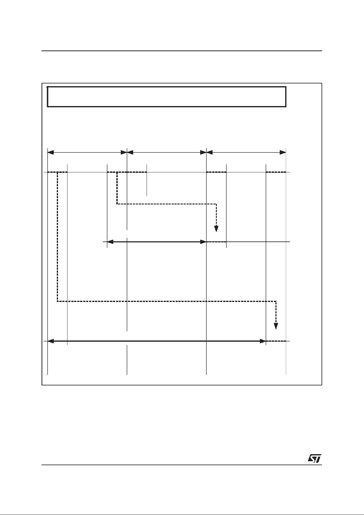
III.2.3 - TimeSlot Assigner Memory
Each HDLC channel is bidirectional and configurateby theTime Slot Assigner(TSA).
TheTSAis amemoryof32words(oneper physical
TimeSlot)where all ofthe 32 inputand outputtime
slots of the HDLC controllers can be associated
to logical HDLC channels. Super channels are
created by assigning the same logical channel
numberto severalphysicaltime slots.
The following features are configurate for each
HDLC time slot :
- Time slot used or not
- One logicalchannel number
- Its source : (DIN8 or the output7 of the matrix)
- Its bit rate and concerned bits (4kbit/s to
64kbit/s). 4kbit/s correspond to one bit transmitted each two frames. This bit mustbe presentin
two consecutive frames in reception, and repeated twice in transmission.
- Its destination:
- direct output on DOUT6
- direct output on DOUT6 and on the Contention
Bus(CB)
- on another OTDM via input7 of the matrix and
on the ContentionBus (CB)
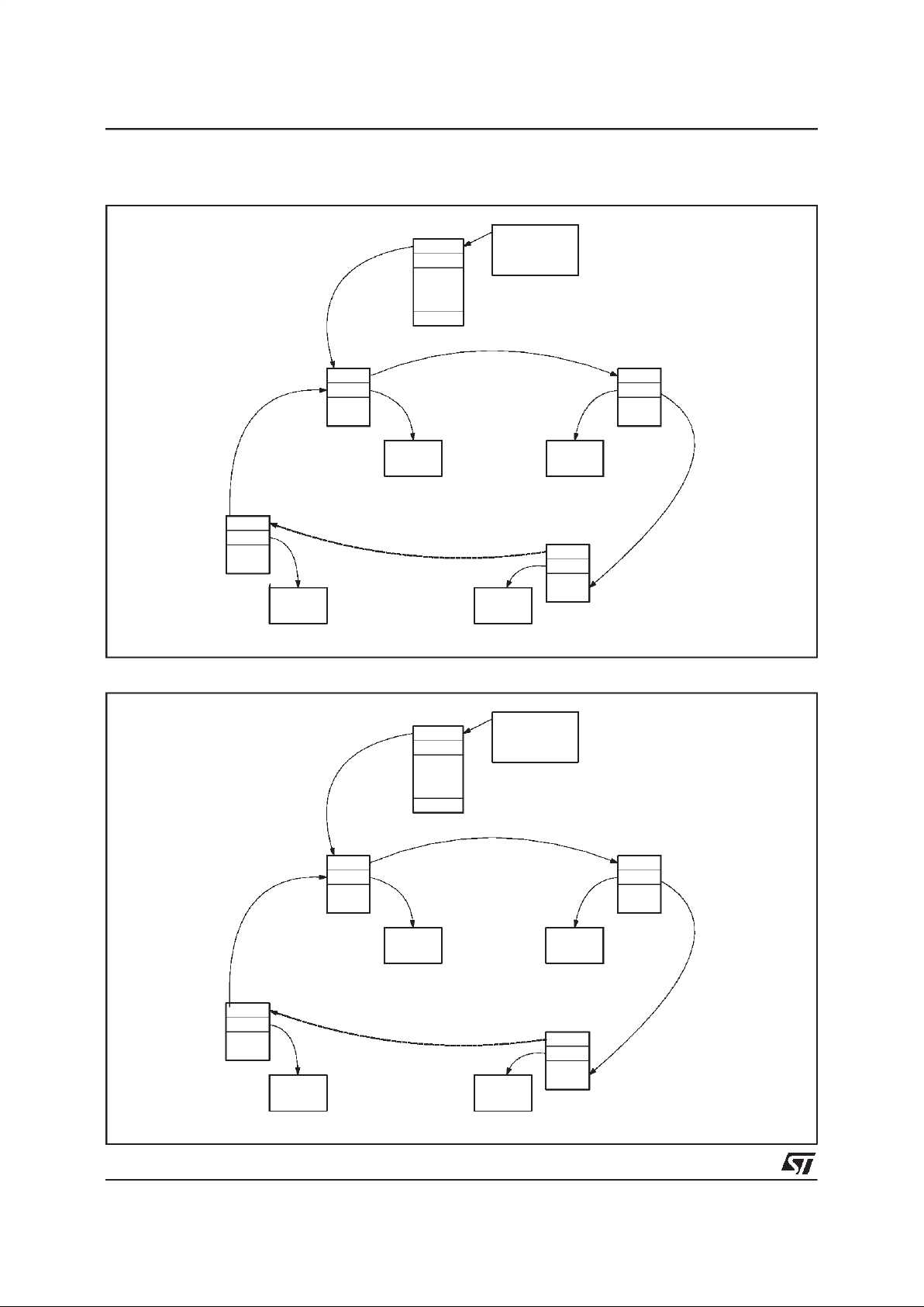
III.2.4 - Data StorageStructure
Dataassociatedwitheach Rx andTxHDLCchannelis storedin externalmemory;Thedatatransfers
between the HDLC controllers and memory are
ensuredby32 DMAC(DirectMemoryAccessController)in reception and 32 DMAC in transmission.
The storage structure chosen in both directionsis
composed of one circular queue of buffers per
channel. In such a queue, each data buffer is
pointedto bya Descriptorlocatedinexternalmemory too. The main information contained in the
Descriptor is the address of the Data Buffer, its
length and the address of the next Descriptor; so
the descriptors can belinked together.
This structure allows to :
- Store receive frames of variable and unknown
length
- Read transmitframes storedin externalmemory
by the host
- Easily performthe frame relay function.
III.2.4.1- Reception
At the initializationof the application, the host has
to prepare an Initialization Block memory, which
containsthe first receivebuffer descriptoraddress
for each channel, and the receivecircularqueues.
At the opening of a receive channel, the DMA
controller reads the address of the first buffer descriptorcorrespondingto thischannelintheinitialization Block. Then, the data transfer can occur
without intervention of the processor (see Figure
12 on Page 28).
Anew HDLCframe alwaysbeginsin a new buffer.
A long frame can be split between several buffers
if the buffersizeis not sufficient.All theinformation
concerning the frame and its location in the
circular queue is included in the Receive Buffer
Descriptor:
- The Receive Buffer Address(RBA),
- The size of thereceive buffer (SOB),
- Thenumberof byteswritteninto thebuffer(NBR),
- The Next Receive DescriptorAddress(NRDA),
- The status concerningthe receiveframe,
- The control of the queue.
III.2.4.2- Transmission
In transmission, the data is managed by a similar
structure as in reception (see Figure 13 on
Page 28).
By the same way, a framecan be splitup between
consecutivetransmit buffers.
The main information contained in the Transmit
Descriptorare :
- transmitbufferaddress (TBA),
- numberof bytesto transmit(NBT)concerningthe
buffer,
- next transmit descriptoraddress (NTDA),
- statusof the frame after transmission,
- control bit of the queue,
- CSMA/CR priority(8 or 10).
III.2.4.3- Frame Relay
The principle of the frame relay is to transmit a
frame which has been received withouttreatment.
A new heading is just added. This will be easily
achieved,takingintoaccount that the queue structure allows the transmission of a frame split between several buffers.
III - FUNCTIONALDESCRIPTION (continued)
STLC5465B
27/101
RECEIVE
DMA
CONTROLLER
RDA0
RDA1
Initialization Block
up to32 channels
RDA31
Receive
Buffer n
Receive
Descriptorn
NRDA
RBA
Receive
Buffer 2
NRDA
RBA
Receive
Descriptor 2
Receive
Buffer 1
NRDA
RBA
Initial Receive
Descriptor
Receive
Buffer 3
Receive
Descriptor3
NRDA
RBA
One receivecircular queue by channel
5464-10.EPS
Figure12 : Structureof the ReceiveCircular Queue
III - FUNCTIONALDESCRIPTION (continued)
TRANSMIT
DMA
CONTROLLER
TDA0
TDA1
Initialization Block
up to32 channels
TDA31
Transmit
Buffer n
Transmit
Descriptor n
NTDA
TBA
Transmit
Buffer 2
NTDA
TBA
Transmit
Descriptor 2
Transmit
Buffer 1
NTDA
TBA
Initial Transmit
Descriptor
Transmit
Buffer 3
Transmit
Descriptor3
NTDA
TBA
One transmitcircular queue by channel
5464-11.EPS
Figure13 : Structureof the TransmitCircular Queue
STLC5465B
28/101

III.2.5 - Transparent Modes
Inthetransparentmode,the
Multi-HDLC
transmits
data in a completely transparent manner without
performingany bit manipulation or Flag insertion.
Thetransparentmodeis per bytefunction.
Two transparentmodes are offered:
- First mode : for the receive channels, the
Multi-HDLC
continuously writes received bytes
into theexternal memory as specifiedin thecurrentreceivedescriptorwithouttakingintoaccount
the Fill CharacterRegister.
- Secondmode:theFil lCharacterRegister specifies
the”fil lcharac ter”whichmustbe takenintoaccount.
Inreception,the”fillcharacter”willnotbetransferred
totheexternalmemory.Thedetectionof”Fillcharacter”marks the end of a messageand generatesan
interruptifBINT=1(seeTransmitDescriptoronPage
95).Whenthe”Fill character”is not detecteda new
messageisreceiving.
As for the HDLC mode the correspondence
between the physical time slot and the logical
channel is fully defined in the Time Slot Assigner
memory(Time slot usedor notused,logicalchannel number,source,destination).
III.2.6 - Commandof the HDLC Channels
The microprocessoris able to control each HDLC
receive and transmit channel. Some of the commands are specific to the transmission or the receptionbut others are identical.
III.2.6.1- ReceptionControl
Theconfigurationof the controlleroperatingmode
is: HDLC mode or Transparentmode.
The control of the controller: START, HALT,CONTINUE,ABORT.
- START: On a start command, the RxDMA controller reads the address of the first descriptor in
the initialization block memory and is ready to
receive a frame.
- HALT: For overloading reasons,themicroprocessor can decideto halt the reception.TheDMA
controllerfinishestransferof the currentframeto
externalmemory and stops. The channel can be
restartedon CONTINUEcommand.
- CONTINUE : The reception restarts in the next
descriptor.
- ABORT:On an abortcommand, the reception is
instantaneously stopped. The channel can be
restartedon a STARTor CONTINUEcommand.
Receptionof FLAG(01111110) or IDLE (11111111)
betweenFrames.
Address recognition. The microprocessordefines
theaddressesthattheRx controllerhastotakeinto
account.
In transparent mode: ”fill character” register selected or not.
III.2.6.2- TransmissionControl
The configurationof the controlleroperatingmode
is : HDLC mode or Transparentmode.
The control of the controller: START, HALT,CONTINUE,ABORT.
- START:Ona startcommand,theTxDMAcontroller reads the address of the firstdescriptor in the
initializationblockmemoryandtries to transmitthe
firstframe if End Of Queueisnotat”1”.
- HALT : The transmitter finishes to sendthe currentframeandstops.Thechannel can be restarted on a CONTINUE command.
- CONTINUE : iftheCONTINUEcommand occurs
after HALTcommand,the HDLC Transmitter restarts by transmittingthe next buffer associated
to the next descriptor.
If the CONTINUE command occurs after an
ABORT command which has occurred during a
frame,theHDLC transmitterrestartsby transmittingthe framewhichhasbeeneffectivelyaborted
by the microprocessor.
- ABORT:On an abortcommand,thetransmission
of the current frame is instantaneouslystopped,
an ABORTsequence”1111111” is sent, followed
by IDLE or FLAG bytes. The channel can be
restartedon a START or CONTINUEcommand.
Transmission of FLAG (01111110) or IDLE
(111111111)betweenframes can be selected.
CRC can be generated or not. If the CRC is not
generated by the HDLC Controller, it must be located in the shared memory.
In transparentmode: ”fillcharacter”registercanbe
selectedor not.
III.3 - C/I and Monitor
III.3.1 - FunctionDescription
The
Multi-HDLC
is abletooperateboth GCIandV*
links. The TDM DIN/DOUT 4 and 5 are internally
connected to the CI and Monitor receivers/transmitters.Sincethecontrollershandleupto 16CIand
16 Monitor channels simultaneously, the
Multi-
HDLC
can manage upto 16 level1 circuits.
The
Multi-HDLC
canbeusedto supporttheCI and
monitor channels based on the following protocols :
- ISDN V* protocol
- ISDN GCI protocol
- Analog GCI protocol.
III - FUNCTIONALDESCRIPTION (continued)
STLC5465B
29/101
III.3.2 - GCIand V*Protocol
ATDM can carry8 GCI channels or V* channels. The monitor and S/C bytes always stand at the same
positionin the TDM in both cases.
Channel 0
Channel 1 to Channel 30
Channel 31
TS0 TS1 TS2 TS3 TS28 TS29 TS30 TS31
B1 B2 MON S/C B1 B2 MON S/C
III - FUNCTIONALDESCRIPTION (continued)
The GCI or V* channelsare composedof 4 bytes
and have both the samegeneral structure.
B1 B2 MON S/C
B1,B2 : Bytes of data. Those bytes are not
affectedby themonitorand CIprotocols.
MON : Monitor channel for operation and
maintenanceinformation.
S/C : Signallingand controlinformation.
Only Monitor handshakes and S/C bytes are dif-
ferentin the threeprotocols:
ISDN V* S/C byte
D C/I 4 bits T E
ISDN GCI S/C byte
D C/I 4 bits A E
AnalogGCIS/C byte
C/I 6 bits A E
CI : The Command/Indicate channel is used for
activation/deactivation of lines and control
functions.
D : These 2 bits carry the 16 kbit/s ISDN basic
accessD channel.
In GCI protocol, A and E are the handshake bits
and are used to controlthe transfer of information
on monitor channels.TheE bit indicates the transfer of each new byte in one directionand the Abit
acknowledgesthis byte transfer in the reverse direction.
InV*protocol,thereisn’t anyhandshakemode.The
transmitter has only to mark the validity of the
Monitorbyte by positioningtheE bit (Tis not used
and is forcedto ”1”).
For more information about the GCI and V*, refer
to the General Interface Circuit Specification (issue1.0, march 1989) and the France Telecom
Specification about ISDN Basic Access second
generation(November 1990).
III.3.3 - Structure of the Treatment
GCI/V* TDM’s are connected to DIN 4 and DIN 5.
The D channels are switched through the matrix
towards the output 7 and the HDLC receiver. The
Monitorand S/C bytesare multiplexedand sent to
the CI and Monitor receivers (see Figure 14 on
Page 31).
In transmission, the S/C and Monitor bytes are
recombined by multiplexing the information providedbytheMonitor,C/IandtheHDLCTransmitter.
Likeinreception,theDchannelisswitchedthrough
the matrix.
III.3.4 - CIand Monitor Channel Configuration
Monitorchannel data is located in a timeslot ; the
CI and monitorhandshakebits arein the next time
slot.
Each channel can be defined independently. A
table with all the possible configurations is presentedhereafter (Table 13).
Table13 : C/I and MON Channel Configuration
C/I validated or not
CI For analog subscriber (6 bits)
CI For ISDN subscriber (4 bits)
Monitor validated
or not
Monitor V*
Monitor GCI
Note : A mix of V* and GCI monitoring can be performed for two
distinct channels in the same application.
III.3.5- CI and Monitor Transmission/Reception
Command
The reception of C/I and Monitor messages are
managedby two interrupt queues.
In transmission, a transmit command register is
implementedforeach C/Iand monitorchannel (16
C/I transmit command registers and 16 Monitor
transmit command registers). Those registers are
accessible in read and write modes by the microprocessor.
STLC5465B
30/101
 Loading...