

STLC5464
MULTI-HDLC
.
32 TxHDLCs WITH BROADCASTING CAPABILITY AND/OR CSMA/CR FUNCTION WITH
AUTOMATIC RESTART IN CASE OF TX
FRAMEABORT
.
32 RxHDLCs INCLUDING ADDRESS RECOGNITION
.
16 COMMAND/INDICATE CHANNELS (4 OR
6-BITPRIMITIVE)
.
16 MONITOR CHANNELS PROCESSED IN
ACCORDANCE WITH GCIOR V*
.
256 x 256 SWITCHING MATRIX WITHOUT
BLOCKING AND WITH TIME SLOT SEQUENCE INTEGRITY AND LOOPBACK PER
BIDIRECTIONALCONNECTION
.
DMA CONTROLLER FOR 32 Tx CHANNELS
AND32 Rx CHANNELS
.
HDLCs AND DMA CONTROLLER ARE CAPABLE OF HANDLING A MIX OF LAPD, LAPB,
SS7,CASANDPROPRIETARYSIGNALLING S
WITH n x 64SWITCHINGMATRIX ASSOCIATED
DESCRIPTION
The STLC5464 is a Subscriberline interface card
controller for Central Office, Central Exchange,
NT2 and PBX capable of handling:
- 16 U Interfacesor
- 2 Megabitsline interface cards or
- 16 SLICs(Plain Old TelephoneService) or
- Mixed analogue and digital Interfaces(SLICs or
U Interfaces)or
- 16 S Interfaces
- SwitchingNetwork with centralized processing
.
EXTERNALSHARED MEMORYACCESSBETWEEN DMA CONTROLLER AND MICROPROCESSOR
.
SINGLE MEMORY SHARED BETWEEN
nx
MULTI-HDLC
PROCESSOR ALLOWS TO HANDLE n x 32
CHANNELS
.
BUSARBITRATION
.
INTERFACE FOR VARIOUS 8,16 OR 32 BIT
MICROPROCESSORS
.
RAM CONTROLLER ALLOWS TO INTERFACEUP TO :
-16MEGABYTESOF DYNAMIC RAM OR
-1 MEGABYTEOF STATIC RAM
.
INTERRUPT CONTROLLER TO STORE
AUTOMATICALLY EVENTS IN SHARED
MEMORY
.
PQFP160PACKAGE
May 1997
s AND SINGLE MICRO-
PQFP160
(Plastic Quad Flat Pack)
ORDER CODE : STLC5464
1/83

STLC5464
CONTENTS Page
I PIN INFORMATION .................................................... 8
I.1 PIN CONNECTIONS . . . . . . . . . . .. .. . .. .. . . . ............................. 8
I.2 PIN DESCRIPTION . . . . ................................................ 9
I.3 PIN DEFINITION . . .. . . . . . . . . .. . . . .. . . . . . . . . ........................... 13
I.3.1 Input Pin Definition . .................................................... 13
I.3.2 OutputPin Definition . . . . . . . .. . . . .. . .. .. . . . ............................. 13
I.3.3 Input/OutputPin Definition . .............................................. 13
II BLOCK DIAGRAM .................................................... 14
III FUNCTIONAL DESCRIPTION ........................................... 15
III.1 THE SWITCHINGMATRIX N x 64KBits/S . . .. . . . .. ......................... 15
III.1.1 FunctionDescription . . .. . .. .. . . . . . . . . .. . . . ............................. 15
III.1.2 Architectureof the Matrix . . . . . . . . . . . . .. . . . .. .. .. ......................... 15
III.1.3 ConnectionFunction . . . . . .. .. . . . . . . . . .. . . . ............................. 15
III.1.4 Loop Back Function . . . . ................................................ 15
III.1.5 Delay through the Matrix . . . . . . . . . . . . .. . . . .. . . . . ......................... 17
III.1.5.1 Variable Delay Mode . . . . ............................................. 17
III.1.5.2 Sequence Integrity Mode . . .. .......................................... 17
III.1.6 ConnectionMemory . . .. ................................................ 21
III.1.6.1 Description . . . . . . . .. . . . .. . . . .. . . . . . ................................. 21
III.1.6.2 Accessto ConnectionMemory . . .. . . . .. . .. .............................. 21
III.1.6.3 Accessto DataMemory . .............................................. 21
III.2 HDLC CONTROLLER . ................................................. 21
III.2.1 Functiondescription . . .. ................................................ 21
III.2.1.1 Format of theHDLC Frame . ........................................... 21
III.2.1.2 Compositionof anHDLC Frame . . .. .................................... 21
III.2.1.3 Descriptionand Functions of theHDLC Bytes . .. . . . . . . . . .. . . . .. .. . .. ....... 23
III.2.2 CSMA/CRCapability . . . . . . . . . . .. .. . .. .. . . . ............................. 23
III.2.3 Time Slot Assigner Memory . . .. .......................................... 24
III.2.4 Data Storage Structure . . .. ............................................. 24
III.2.4.1 Reception . . .. ...................................................... 24
III.2.4.2 Transmission . . . . ................................................... 24
III.2.4.3 Frame Relay . ....................................................... 24
III.2.5 TransparentModes . . . . ................................................ 26
III.2.6 Commandof the HDLC Channels . ........................................ 26
III.2.6.1 Reception Control . . .. ................................................ 26
III.2.6.2 TransmissionControl . . .. ............................................. 26
III.3 C/I AND MONITOR . . .. ................................................ 26
III.3.1 FunctionDescription . . .. . .. .. . . . . . . . . .. . . . ............................. 26
III.3.2 GCI and V* Protocol . . .. ................................................ 27
III.3.3 Structureof the Treatment . .............................................. 27
III.3.4 CI and Monitor ChannelConfiguration . ..................................... 27
III.3.5 CI and Monitor Transmission/ReceptionCommand . .. . .. .. . . . . . . . . .. .. . .. .... 27
III.4 MICROPROCESSOR INTERFACE . . .. .................................... 28
III.4.1 Description . .......................................................... 28
III.4.2 Definition of the Interfacefor thedifferent microprocessors . . . .. . . .. ............. 28
2/83

STLC5464
CONTENTS
III.5 MEMORYINTERFACE . . . . ............................................. 31
III.5.1 FunctionDescription . . .. . .. .. . . . . . . . . .. . . . ............................. 31
III.5.2 Choiceof memoryversus microprocessorand capacity required . . . . . . ........... 31
III.5.3 MemoryCycle . ....................................................... 31
III.5.4 SRAM interface . . . . ................................................... 32
III.5.4.1 18K x n SRAM . . .. . .. .. . . . . . . . . . . . . . . . . . . ........................... 32
III.5.4.2 512K x n SRAM . .................................................... 32
III.5.5 DRAM Interface . . .. ................................................... 32
III.5.5.1 256K x n DRAM . .................................................... 32
III.5.5.2 1M x n DRAM . . . . ................................................... 33
III.5.5.3 4M x n DRAM . . . . ................................................... 33
III.6 BUS ARBITRATION . . .. ................................................ 33
III.7 CLOCK SELECTIONAND TIME SYNCHRONIZATION . . . .. . .. .. . .. . .. .. . . . . . . 34
III.7.1 ClockDistributionSelection and Supervision. . .. . . . . . . . . . . . . .. .. . .. .......... 34
III.7.2 VCXOFrequency Synchronization. ........................................ 34
III.8 INTERRUPTCONTROLLER . . . . . . . . . . . . .. . . . . . . . . . ...................... 35
III.8.1 Description . .......................................................... 35
III.8.2 OperatingInterrupts(INT0 Pin) . . . . ....................................... 35
III.8.3 Time Base Interrupts (INT1 Pin) . . .. . . . . . . . . .............................. 35
III.8.4 EmergencyInterrupts(WDO Pin) . . ........................................ 35
III.8.5 InterruptQueues . . . . . . . .. . .. .. . .. .. . . .. . . . . ........................... 35
III.9 WATCHDOG . . . . . . . . . . . . .. . . . .. . . . . . ................................. 36
III.10 RESET . . . . . . ...................................................... .. 36
(continued)
Page
IV DC SPECIFICATIONS .................................................. 37
V CLOCK TIMING ....................................................... 38
V.1 SYNCHRONIZATION SIGNALSDELIVEREDBY THE SYSTEM . . . . . . ........... 38
V.2 TDM SYNCHRONIZATION . . . . .......................................... 39
V.3 GCI INTERFACE . . .. . . . .. . . . .. . . . .. . . . . . . . . ........................... 40
V.4 V* INTERFACE . . . . ................................................... 41
VI MEMORYTIMING ..................................................... 42
VI.1 DYNAMICMEMORIES . . .. ............................................. 42
VI.2 STATICMEMORIEs . . .. . .. .. . . . . . . . . .. . . . ............................. 44
VII MICROPROCESSOR TIMING ............................................ 46
VII.1 ST9 FAMILY MOD0=1, MOD1=0, MOD2=0 . . . . . . . . .. . .. . .. .. . . . . . .......... 46
VII.2 80C188MOD0=1, MOD1=1,MOD2=0 . . .. ................................. 48
VII.3 80C186MOD0=1, MOD1=1,MOD2=1 . . .. ................................. 50
VII.4 68000 MOD0=0, MOD1=0,MOD2=1 . . . . . . . .. . . . . . . . . . . . . .. ................ 52
VII.5 TOKEN RING TIMING . ................................................. 54
VII.6 MASTERCLOCK TIMING . .............................................. 54
3/83

STLC5464
CONTENTS
VIII INTERNAL REGISTERS ................................................ 55
VIII.1 IDENTIFICATION ANDDYNAMIC COMMAND REGISTER . . . .. . .. . .. IDCR (00)H 55
VIII.2 GENERALCONFIGURATION . ................................. GCR(02)H 55
VIII.3 INPUTMULTIPLEXCONFIGURATION REGISTER0. . . . .. .........IMCR0(04)H 57
VIII.4 INPUTMULTIPLEXCONFIGURATION REGISTER1. . . . .. .........IMCR1(06)H 57
VIII.5 OUTPUTMULTIPLEXCONFIGURATION REGISTER0. .. . . . . . . . . . OMCR0(08)H 57
VIII.6 OUTPUTMULTIPLEXCONFIGURATION REGISTER1. .. . . . . . . . . OMCR1 (0A)H 58
VIII.7 SWITCHING MATRIXCONFIGURATION REGISTER. . . . .. .........SMCR (0C)H 58
VIII.8 CONNECTION MEMORYDATA REGISTER. . .. . . . . .. . .. . .. .. . . . . CMDR(0E)H 59
VIII.9 CONNECTION MEMORYADDRESS REGISTER. .. . .. ............ CMAR (10)H 60
VIII.10 SEQUENCEFAULT COUNTERREGISTER . . . . . . . . .. . .. . .. .. . . . . SFCR(12)H 61
VIII.11 TIME SLOT ASSIGNERADDRESSREGISTER . . . . .. .. . . . . . . . . .. . TAAR (14)H 61
VIII.12 TIME SLOT ASSIGNERDATA REGISTER . . .. .. . .. .............. TADR (16)H 62
VIII.13 HDLC TRANSMIT COMMANDREGISTER . . . . . . . . . .............. HTCR (18)H 62
VIII.14 HDLC RECEIVE COMMAND REGISTER . ....................... HRCR (1A)H 64
VIII.15 ADDRESSFIELD RECOGNITIONADDRESSREGISTER . . . .. . . . . . AFRAR (1C)H 65
VIII.16 ADDRESSFIELD RECOGNITIONDATA REGISTER . . . . .. ........ AFRDR(1E)H 66
VIII.17 FILL CHARACTER REGISTER . . . . ............................. FCR(20)H 66
VIII.18 GCI CHANNELSDEFINITION REGISTER 0 . . .. .. .. . . . . . . . . .. .. . . GCIR0 (22)H 66
VIII.19 GCI CHANNELSDEFINITION REGISTER 1 . . .. .. .. . . . . . . . . .. .. . . GCIR1 (24)H 67
VIII.20 GCI CHANNELSDEFINITION REGISTER 2 . . .. .. .. . . . . . . . . .. .. . . GCIR2 (26)H 67
VIII.21 GCI CHANNELSDEFINITION REGISTER 3 . . .. .. .. . . . . . . . . .. .. . . GCIR3 (28)H 67
VIII.22 TRANSMITCOMMAND / INDICATE REGISTER. . . . .. .. . . . . . . . . .. . . TCIR (2A)H 68
VIII.23 TRANSMITMONITOR ADDRESS REGISTER . . . . . .. .. ........... TMAR(2C)H 69
VIII.24 TRANSMITMONITOR DATA REGISTER . ....................... TMDR(2E)H 70
VIII.25 TRANSMITMONITOR INTERRUPTREGISTER. .. . . . .. .. . .. . .. .. . . TMIR (30)H 70
VIII.26 MEMORYINTERFACECONFIGURATIONREGISTER . .. . .. .. . . . . . . MICR(32)H 70
VIII.27 INITIATEBLOCKADDRESS REGISTER. . . . . . . ................... IBAR (34)H 72
VIII.28 INTERRUPTQUEUESIZE REGISTER. . .. ....................... IQSR(36)H 72
VIII.29 INTERRUPTREGISTER . . .. . .. .. . . . . . . . . .. . . .. ................. IR(38)H 73
VIII.30 INTERRUPTMASK REGISTER. . .. .............................. IMR(3A)H 74
VIII.31 TIME REGISTER . . . . . . . .. . .. .. . .. .. . . .. . . . . ................ TIMR(3C)H 74
VIII.32 TESTREGISTER . . .. . . . .. . .. .. . . . . . . . . . . . .. ................... TR(3E)H 74
(continued)
Page
4/83

STLC5464
CONTENTS
IX EXTERNALREGISTERS ............................................... 75
IX.1 NITIALIZATIONBLOCK IN EXTERNALMEMORY . . . . . . . .. ................... 75
IX.2 RECEIVEDESCRIPTOR . . .. . . . .. . .. .. . . . . . . . .. ......................... 76
IX.2.1 Bits writtenby the Microprocessoronly . . . . ................................. 76
IX.2.2 Bits writtenby the Rx DMAConly . ........................................ 76
IX.2.3 Receive Buffer . ....................................................... 76
IX.3 TRANSMITDESCRIPTOR . . .. .......................................... 77
IX.3.1 Bits writtenby the Microprocessoronly . . . . ................................. 77
IX.3.2 Bits writtenby the Rx DMAConly . ........................................ 78
IX.3.3 TransmitBuffer . ....................................................... 78
IX.4 RECEIVE& TRANSMIT HDLC FRAME INTERRUPT . . . . . . .................... 78
IX.5 RECEIVECOMMAND/ INDICATE INTERRUPT . . .. .. ....................... 79
IX.5.1 Receive Command / IndicateInterrupt when TSV = 0 . . . . . . .................... 79
IX.5.2 Receive Command / IndicateInterrupt when TSV = 1 . . . . . . .................... 80
IX.6 RECEIVEMONITORINTERRUPT . . . . .................................... 80
IX.6.1 Receive Monitor Interrupt when TSV = 0 . . . . . . . ............................. 80
IX.6.2 Receive Monitor Interrupt when TSV = 1 . . . . . . . ............................. 81
X PACKAGE MECHANICAL DATA ......................................... 82
(continued)
Page
5/83

STLC5464
LISTOF FIGURES Page
I PIN INFORMATION .................................................... 8
II BLOCK DIAGRAM .................................................... 14
Figure1 : General Block Diagram . . .. . . . .. . . . . . . . .. .. . .. ................ 14
III FUNCTIONAL DESCRIPTION ........................................... 15
Figure2 : SwitchingMatrix Data Path . . .. . . . ............................. 16
Figure3 : Unidirectionaland BidirectionalConnections . .. .. . . .. ............. 17
Figure4 : LoopBack . . . . ............................................. 17
Figure5 : Variable Delay through the matrix with ITDM= 1 . .. .. . . .. .......... 18
Figure6 : Variable Delay through the matrix with ITDM= 0 . .. .. . . .. .......... 19
Figure7 : Constant Delay throughthe matrixwith SI = 1 . . . . . . .. .. . .. . .. .. . . . 20
Figure8 : HDLC and DMA ControllerBlock Diagram . .. . . . . . . . . .. .. . .. . .. .. . 22
Figure9 : Structureof theReceive CircularQueue . . . .. . . .. ................ 25
Figure10 : Structureof theTransmitCircular Queue . . . . . . . .. ................ 25
Figure11 : D, C/Iand Monitor Channel Path . . . . . . . .. ...................... 28
Figure12 :
Figure13 :
Figure14 : MicroprocessorInterface for INTEL80C188 . . . . .. ................. 29
Figure15 : MicroprocessorInterface for INTEL80C186 . . . . .. ................. 29
Figure16 : MicroprocessorInterface for MOTOROLA 68000 . . . . . . . .. .......... 30
Figure17 : MicroprocessorInterface for ST9 . . . . . . . .. ...................... 30
Figure18 : 128K x 8 SRAMCircuit Memory Organization . .. .. . .. . .. .. . . . . . . . . 32
Figure19 : 512K x 8 SRAMCircuit Memory Organization . .. .. . .. . .. .. . . . . . . . . 32
Figure20 : 256K x 16 DRAMCircuit Organization . .. . . . .. .. . .. . .. .. . . . . . .... 32
Figure21 : 1M x 16 DRAM Circuit Organization . . . . .. ....................... 33
Figure22 : 4M x 16 DRAM Circuit Organization . . . . .. ....................... 33
Figure23 : Chain of n
Figure24 : MHDLC Clock Generation. . . . ................................. 34
Figure25 : VCXO FrequencySynchronization . . . . . . . . . . . .. .. . .. . .. .. ....... 35
Figure26 : The Three Circular Interrupt Memories . . . . .. .. . . . . . . . . .. .. . .. .... 36
Multi-HDLC
Multi-HDLC
connectedto µP with multiplexed buses . . . .. . . . . ....... 29
connectedto µP with non-multiplexedbuses . . . . .. .. . . . . 29
Multi-HDLC
Components . . . . . . ....................... 33
IV DC SPECIFICATIONS .................................................. 37
V CLOCK TIMING ....................................................... 38
Figure27 : Clocks received and deliveredby the
Figure28 : SynchronizationSignals receivedby the
Figure29 : GCI Synchro Signal delivered by the
Figure30 : V* SynchronizationSignal delivered by the
VI MEMORYTIMING ..................................................... 42
Figure31 : Dynamic Memory Read Signals from the
Figure32 : Dynamic Memory Write Signalsfrom the
Figure33 : Static MemoryRead Signals from the
Figure34 : Static MemoryWrite Signals from the
6/83
Multi-HDLC
Multi-HDLC
Multi-HDLC
Multi-HDLC
Multi-HDLC
Multi-HDLC
Multi-HDLC
Multi-HDLC
.................. 38
................ 39
................... 40
.............. 41
............... 42
............... 43
.................. 44
.................. 45

STLC5464
LISTOF FIGURES
VII MICROPROCESSOR TIMING ............................................ 46
Figure35 : ST9 Read Cycle . ........................................... 46
Figure36 : ST9 Write Cycle . ........................................... 47
Figure37 : 80C188 Read Cycle . ........................................ 48
Figure38 : 80C188 WriteCycle . ........................................ 49
Figure39 : 80C186 Read Cycle . ........................................ 50
Figure40 : 80C186 WriteCycle . ........................................ 51
Figure41 : 68000 Read Cycle . .. .. . . . . .................................. 52
Figure42 : 68000 Write Cycle . . . . ....................................... 53
Figure43 : Token Ring . . . . . . . . . . .. .. . . . . . . . .. ......................... 54
Figure44 : MasterClock . .............................................. 54
VIII INTERNAL REGISTERS ................................................ 55
IX EXTERNALREGISTERS ............................................... 75
X PACKAGE MECHANICAL DATA ........................................ 82
(continued)
Page
7/83
STLC5464
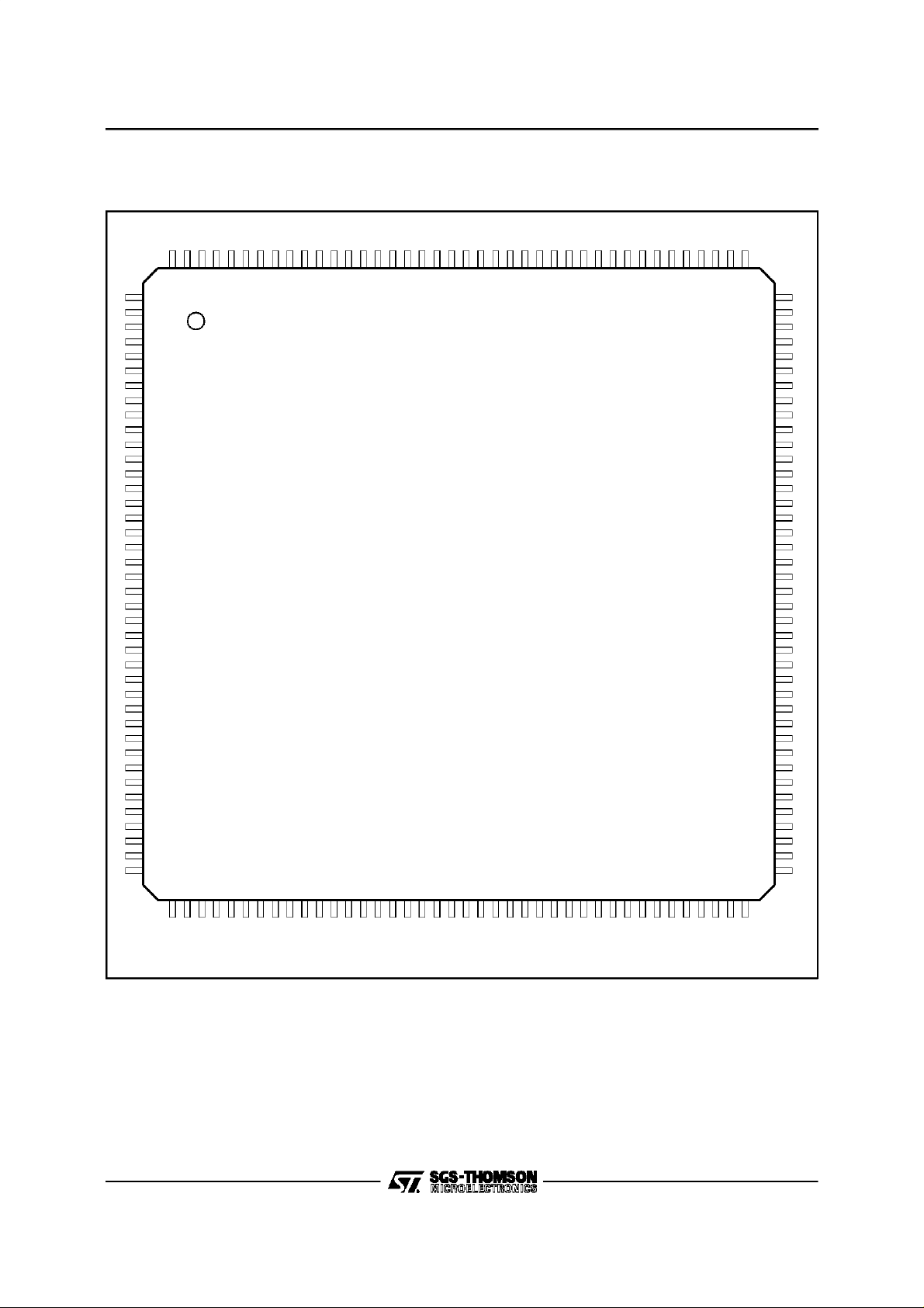
I - PIN INFORMATION
I.1 - Pin Connections
SSVDD
NTEST
V
160
159
NRESET
1
XTAL1
2
XTAL2
3
WDO
4
CB
5
EC
6
VCXO IN
7
VCXO OUT
8
9
DCLK
10
CLOCKA
11
CLOCKB
12
FRAMEA
13
FRAMEB
14
V
DD
15
V
SS
16
FS
17
FSCG
18
FSCV
19
PSS
20
DIN0
21
DIN1
22
DIN2
23
DIN3
24
DIN4
25
DIN5
26
DIN6
27
DIN7
28
DIN8
29
V
DD
30
V
SS
31
DOUT0
32
DOUT1
33
DOUT2
34
DOUT3
35
DOUT4
36
DOUT5
37
DOUT6
38
DOUT7
39
NDIS
40
NTRST
158
DM15
157
DM14
156
DM13
155
DM12
154
DM11
153
DM10
152
DM9
151
DM8
150
414243444546474849505152535455565758596061626364656667686970717273747576777879
DM7
149
DM6
148
DM5
147
SSVDD
V
146
145
DM4
144
DM3
143
DM2
142
DM1
141
DM0
140
ADM14
ADM13
139
138
ADM12
ADM11
137
136
VSSV
ADM10
135
134
133
DD
ADM9
ADM8
ADM7
ADM6
ADM5
ADM4
ADM3
ADM2
132
131
130
129
128
127
126
125
ADM1
ADM0
124
123
NRAS3/NCE6
NRAS2/NCE4
NCAS1/NCE3
NRAS1/NCE2
NCAS0/NCE1
NRAS0/NCE0
A23/ADM18
A22/ADM17
A21/ADM16
A20/ADM15
VSSV
122
DD
121
NCE7
NCE5
NOE
NWE
TRO
TRI
D15
D14
D13
D12
D11
D10
A19
A18
A17
A16
120
119
118
117
116
115
114
113
112
111
110
109
108
V
SS
107
V
DD
106
105
104
103
102
101
100
D9
99
D8
98
D7
97
D6
96
D5
95
D4
94
D3
93
D2
92
D1
91
D0
90
V
SS
89
V
DD
88
87
86
85
84
83
82
81
80
8/83
TMS
TDI
TDO
TCK
SS
DD
V
V
NCS0
NCS1
INT0
INT1
NLDS
NBHE/NUDS
READY
NDTACK
NAS/ALE
R/W / NWR
MOD0
NDS/NRD
MOD1
MOD2
SS
DD
V
V
A0/AD0
A1/AD1
A2/AD2
A3/AD3
A4/AD4
A5/AD5
A6/AD6
A7/AD7
A8/AD8
A9/AD9
SS
DD
V
V
A10/AD10
A11/AD11
A12/AD12
A13/AD13
A14/AD14
A15/AD15
5464-01.EPS
STLC5464
I - PIN INFORMATION(continued)
I.2 - Pin Description
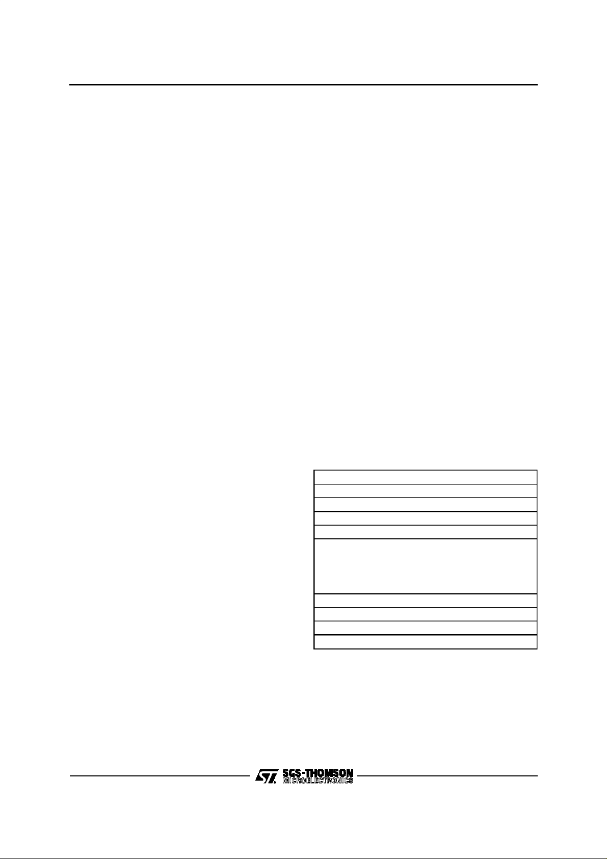
Pin N° Symbol Type Function
POWER PINS (all thepower and ground pins must be connected)
14 V
15 V
29 V
30 V
45 V
46 V
61 V
62 V
73 V
74 V
89 V
90 V
107 V
108 V
121 V
122 V
133 V
134 V
145 V
146 V
158 V
159 V
DD1
SS1
DD2
SS2
DD3
SS3
DD4
SS4
DD5
SS5
DD6
SS6
DD7
SS7
DD8
SS8
DD9
SS9
DD10
SS10
DD11
SS11
CLOCKS
2 XTAL1 I Crystal 1. A clockpulse at f
3 XTAL2 O Crystal 2. If the internal crystal oscillator is used, the second crystal pin isapplied
7 VCXO IN O4 VCXO input signal. This signal is compared to clock A(or B) selected inside the
8 VCXO OUT I3 VCXO error signal. This pin delivers the result of the comparison.
10 CLOCKA I3 Input Clock A (4096kHz or 8192kHz)
11 CLOCKB I3 Input Clock B (4096kHz or 8192kHz)
12 FRAMEA I3 Clock A at 8kHz
13 FRAMEB O8 Clock B at 8kHz
9 DCLK O8 Data Clock issuedfrom Input Clock A (or B). This clock is delivered by the circuit
17 FSCG O8 Frame synchronization for GCI at 8kHz. This clockis issued from FRAME A (or B).
18 FSCV* I3 Frame synchronization for V Star at 8kHz
16 FS O8 Frame synchronization.This signal synchronizesDIN0/7 and DOUT0/7.
19 PSS I3 Programmable synchronization Signal. The PS bit of connection memory is read
Type : I1 = Input TTL ; I2 = I1 + Pull-up ; I3 = I1 + Hysteresis ; I4 = I3 + Pull-up ;
O4 = Output CMOS 4mA ; O4T = O4 + Tristate ; O8 = Output CMOS 8mA, ”1” and ”0” at Low Impedance ;
O8D = OutputCMOS 8mA,Open Drain ; O8DT = Output CMOS 8mA, Open Drainor Tristate;
O8T = OutputCMOS 8mA, Tristate
Power DC supply
Ground DC ground
Power DC supply
Ground DC ground
Power DC supply
Ground DC ground
Power DC supply
Ground DC ground
Power DC supply
Ground DC ground
Power DC supply
Ground DC ground
Power DC supply
Ground DC ground
Power DC supply
Ground DC ground
Power DC supply
Ground DC ground
Power DC supply
Ground DC ground
Power DC supply
Ground DC ground (Total22)
of two crystal pins) with : -50.10
to this output.
Multi-HDLC
.
at 4096kHz(or2048kHz). DOUT0/7 aretransmittedon the risingedge of thissignal.
DIN0/7 are sampled on the fallingedge of this signal.
in real time.
= 32000kHz can be applied to this input (or one pin
Min.
-6
< ∆f < +50.10-6.
9/83
STLC5464
I - PIN INFORMATION(continued)
I.2 - Pin Description (continued)
Pin N° Symbol Type Function
TIMEDIVISION MULTIPLEXES (TDM)
20 DIN0 I1 TDM0Data Input 0
21 DIN1 I1 TDM1Data Input 1
22 DIN2 I1 TDM2Data Input 2
23 DIN3 I1 TDM3Data Input 3
24 DIN4 I1 TDM4Data Input 4
25 DIN5 I1 TDM5Data Input 5
26 DIN6 I1 TDM6Data Input 6
27 DIN7 I1 TDM7Data Input 7
28 DIN8 I1 TDM8Data Input 8
31 DOUT0 O8DT TDM0 Data Output0
32 DOUT1 O8DT TDM1 Data Output1
33 DOUT2 O8DT TDM2 Data Output2
34 DOUT3 O8DT TDM3 Data Output3
35 DOUT4 O8DT TDM4 Data Output4
36 DOUT5 O8DT TDM5 Data Output5
37 DOUT6 O8DT TDM6 Data Output6
38 DOUT7 O8DT TDM7 Data Output7
39 NDIS I1 DOUT 0/7 Not Disable. When this pin is at 0V, the Data Output 0/7 are at high
5 CB O8D Contention Bus for CSMA/CR
6 EC I1 Echo. Wired at VSS if not used.
BOUDARY SCAN
40 NTRST I4 Reset for boundary scan
41 TMS I2 Mode Selection for boundary scan
42 TDI I2 Input Data for boundary scan
43 TDO O4 Output Datafor boundary scan
44 TCK I4 Clock for boundary scan
MICROPROCESSOR INTERFACE
58 MOD0 I1 1 1 0 1
59 MOD1 I1 1 1 0 0
60 MOD2 I1 0 1 1 0
1 NRESET I3 CircuitReset
47 NCS0 I3 Chip Select 0 : internal registers are selected
48 NCS1 I3 Chip Select 1 : external memory isselected
49 INT0 O4 Interrupt generated by HDLC, RxC/Ior RxMON. Active high.
50 INT1 O4 Interrupt1.This pin goes to 5V when the selected clock A (or B) has disappeared ;
4 WDO O4 Watch Dog Output.This pingoes to5V during1ms when the microprocessor has not
Type : I1 = Input TTL ; I2 = I1 + Pull-up ; I3 = I1 + Hysteresis ; I4 = I3 + Pull-up ;
O4 = Output CMOS 4mA ; O4T = O4 + Tristate ; O8 = Output CMOS 8mA, ”1” and ”0” at Low Impedance ;
O8D = OutputCMOS 8mA,Open Drain ; O8DT = Output CMOS 8mA, Open Drainor Tristate;
O8T = OutputCMOS 8mA, Tristate
impedance. Wired at VDD if not used.
80C188 80C186 68000 ST9
250µs after resetthis pin goesto 5V also if clock A is not present.
reset the Watch Dog during the programmable time.
10/83
I - PIN INFORMATION(continued)
I.2 - Pin Description (continued)
Pin N° Symbol Type Function
MICROPROCESSOR INTERFACE (continued)
51 NLDS I3 Lower Data Strobe (68000)
52 NUDS I3 Bus High Enable (Intel) / Upper Data Strobe(68000)
53 NDTACK O8D Data Transfer Acknowledge (68000)
54 READY O8T Data TransferAcknowledge (Intel)
55 NAS/ALE I3 Address Strobe(Motorola) / Addresss Latch Enable(Intel)
56 R/W / NWR I3 Read/Write (Motorola) /Write(Intel)
57 NDS/NRD I3 Data Strobe (Motorola)/Read Data(Intel)
63 A0/AD0 I/O Address bit 0 (Motorola) / Address/Data bit 0 (Intel)
64 A1/AD1 I/O Address bit 1 (Motorola) / Address/Data bit 1 (Intel)
65 A2/AD2 I/O Address bit 2 (Motorola) / Address/Data bit 2 (Intel)
66 A3/AD3 I/O Address bit 3 (Motorola) / Address/Data bit 3 (Intel)
67 A4/AD4 I/O Address bit 4 (Motorola) / Address/Data bit 4 (Intel)
68 A5/AD5 I/O Address bit 5 (Motorola) / Address/Data bit 5 (Intel)
69 A6/AD6 I/O Address bit 6 (Motorola) / Address/Data bit 6 (Intel)
70 A7/AD7 I/O Address bit 7 (Motorola) / Address/Data bit 7 (Intel)
71 A8/AD8 I/O Address bit 8 (Motorola) / Address/Data bit 8 (Intel)
72 A9/AD9 I/O Address bit 9 (Motorola) / Address/Data bit 9 (Intel)
75 A10/AD10 I/O Address bit 10 (Motorola) / Address/Data bit 10 (Intel)
76 A11/AD11 I/O Address bit 11 (Motorola) / Address/Data bit 11 (Intel)
77 A12/AD12 I/O Address bit 12 (Motorola) / Address/Data bit 12 (Intel)
78 A13/AD13 I/O Address bit 13 (Motorola) / Address/Data bit 13 (Intel)
79 A14/AD14 I/O Address bit14 (Motorola) / Address/Data bit 14 (Intel)
80 A15/AD15 I/O Address bit15 (Motorola) / Address/Data bit 15 (Intel)
81 A16 I1 Address bit16 (Motorola) / Address bit 16 (Intel)
82 A17 I1 Address bit17 (Motorola) / Address bit 17 (Intel)
83 A18 I1 Address bit18 (Motorola) / Address bit 18 (Intel)
84 A19 I1 Address bit19 (Motorola) / Address bit 19 (Intel)
85 A20/ADM15 I/O Address bit 20 from µP (input) / Address bit 15 forSRAM (output)
86 A21/ADM16 I/O Address bit 21 from µP (input) / Address bit 16 forSRAM (output)
87 A22/ADM17 I/O Address bit 22 fromµP (input) / Addressbit 17 for SRAM (output)
88 A23/ADM18 I/O Address bit 23 from µP (input) / Address bit 18 forSRAM (output)
91 DO I/O Data bit 0 for µP ifnot multiplexed (seeNote 1).
92 D1 I/O Data bit 1forµP if not multiplexed
93 D2 I/O Data bit 2for µP if not multiplexed
94 D3 I/O Data bit 3for µP if not multiplexed
95 D4 I/O Data bit 4forµP if not multiplexed
96 D5 I/O Data bit 5for µP if not multiplexed
97 D6 I/O Data bit 6for µP if not multiplexed
98 D7 I/O Data bit 7forµP if not multiplexed
99 D8 I/O Data bit 8for µP if not multiplexed
Type : I1 = Input TTL ; I2 = I1 + Pull-up ; I3 = I1 + Hysteresis ; I4 = I3 + Pull-up ;
O4 = Output CMOS 4mA ; O4T = O4 + Tristate ; O8 = Output CMOS 8mA, ”1” and ”0” at Low Impedance ;
O8D = OutputCMOS 8mA,Open Drain ; O8DT = Output CMOS 8mA, Open Drainor Tristate;
O8T = OutputCMOS 8mA, Tristate
STLC5464
11/83
STLC5464
I - PIN INFORMATION(continued)
I.2 - Pin Description (continued)
Pin N° Symbol Type Function
MICROPROCESSOR INTERFACE (continued)
100 D9 I/O Data bit 9for µP if not multiplexed
101 D10 I/O Data bit 10for µP if not multiplexed
102 D11 I/O Data bit 11forµP if not multiplexed
103 D12 I/O Data bit 12for µP if not multiplexed
104 D13 I/O Data bit 13for µP if not multiplexed
105 D14 I/O Data bit 14forµP if not multiplexed
106 D15 I/O Data bit 15for µP if not multiplexed
MEMORY INTERFACE
109 TRI I3 Token Ring Input (foruse
110 TRO O4 Token Ring Output (for use
111 NWE O4T Write Enable for memory circuits
112 NOE O4T Control Output Enable for memory circuits
113 NRAS0/NCE0 O4T Row Address Strobe Bank0 / Chip Enable0 for SRAM
114 NCAS0/NCE1 O4T Column Address StrobeBank 0 / Chip Enable1 for SRAM
115 NRAS1/NCE2 O4T Row Address Strobe Bank1 / Chip Enable2 for SRAM
116 NCAS1/NCE3 O4T Column Address StrobeBank 1 / Chip Enable 3 for SRAM
117 NRAS2/NCE4 O4T Row Address Strobe Bank2 / Chip Enable4 for SRAM
118 NCE5 O4T Chip Enable 5 for SRAM
119 NRAS3/NCE6 O4T Row Address Strobe Bank3 / Chip Enable6 for SRAM
120 NCE7 O4T Chip Enable 7 for SRAM
123 ADM0 O8T Address bit 0for SRAM and DRAM
124 ADM1 O8T Address bit 1for SRAM and DRAM
125 ADM2 O8T Address bit 2for SRAM and DRAM
126 ADM3 O8T Address bit 3for SRAM and DRAM
127 ADM4 O8T Address bit 4for SRAM and DRAM
128 ADM5 O8T Address bit 5for SRAM and DRAM
129 ADM6 O8T Address bit 6for SRAM and DRAM
130 ADM7 O8T Address bit 7for SRAM and DRAM
131 ADM8 O8T Address bit 8for SRAM and DRAM
132 ADM9 O8T Address bit 9for SRAM and DRAM
135 ADM10 O8T Address bit 10 for SRAM and DRAM
136 ADM11 O8T Address bit 11 for SRAM only
137 ADM12 O8T Address bit 12 for SRAM only
138 ADM13 O8T Address bit 13 for SRAM only
139 ADM14 O8T Address bit 14 for SRAM only
Type : I1 = Input TTL ; I2 = I1 + Pull-up ; I3 = I1 + Hysteresis ; I4 = I3 + Pull-up ;
O4 = Output CMOS 4mA ; O4T = O4 + Tristate ; O8 = Output CMOS 8mA, ”1” and ”0” at Low Impedance ;
O8D = OutputCMOS 8mA,Open Drain ; O8DT = Output CMOS 8mA, Open Drainor Tristate;
O8T = OutputCMOS 8mA, Tristate
Multi-HDLC
Multi-HDLC
s in cascade)
s in cascade)
12/83
STLC5464
I - PIN INFORMATION(continued)
I.2 - Pin Description (continued)
Pin N° Symbol Type Function
MEMORY INTERFACE (continued)
140 DM0 I/O Memory Data bit 0
141 DM1 I/O Memory Data bit 1
142 DM2 I/O Memory Data bit 2
143 DM3 I/O Memory Data bit 3
144 DM4 I/O Memory Data bit 4
147 DM5 I/O Memory Data bit 5
148 DM6 I/O Memory Data bit 6
149 DM7 I/O Memory Data bit 7
150 DM8 I/O Memory Data bit 8
151 DM9 I/O Memory Data bit 9
152 DM10 I/O Memory Data bit 10
153 DM11 I/O Memory Data bit 11
154 DM12 I/O Memory Data bit 12
155 DM13 I/O Memory Data bit 13
156 DM14 I/O Memory Data bit 14
157 DM15 I/O Memory Data bit 15
160 NTEST I2 Test Control. When this pin is at 0V each output is high impedance except XTAL2 Pin.
Type : I1 = Input TTL ; I2 = I1 + Pull-up ; I3 = I1 + Hysteresis ; I4 = I3 + Pull-up ;
O4 = Output CMOS 4mA ; O4T = O4 + Tristate ; O8 = Output CMOS 8mA, ”1” and ”0” at Low Impedance ;
O8D = OutputCMOS 8mA,Open Drain ; O8DT = Output CMOS 8mA, Open Drainor Tristate;
O8T = OutputCMOS 8mA, Tristate
Note : D0/15 input/output pins must be connectedto one single externalpull up resistor if not used.
I.3 - Pin Definition
I.3.1- Input Pin Definition
I1 : Input1 TTL
I2 : Input2 TTL+ pull-up
I3 : Input3 TTL+ hysteresis
I4 : Input4 TTL+ hysteresis +pull-up
I.3.2- Output Pin Definition
O4 : OutputCMOS 4mA
O4T : OutputCMOS4mA, Tristate
O8 : OutputCMOS 8mA
O8T : OutputCMOS8mA,Tristate
O8D : Output CMOS 8mA,OpenDrain
O8DT : OutputCMOS 8mA,Open Drain or Tristate(Programmablepin)
Moreover, each output is high impedance when theNTEST Pin isat 0 volt except XTAL2 Pin.
I.3.3- Input/Output Pin Definition
I/O: InputTTL/ Output CMOS 8mA.
N.B. XTAL1 : this inputis CMOS.
XTAL2 : NTESTpin at 0 hasno effecton thispin.
13/83
STLC5464
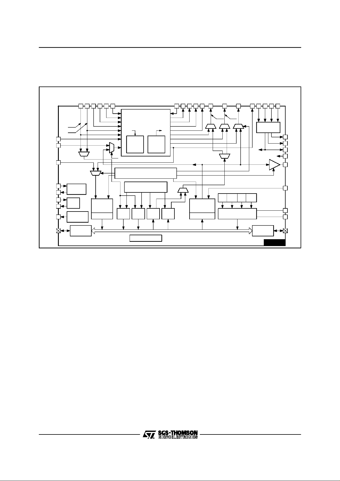
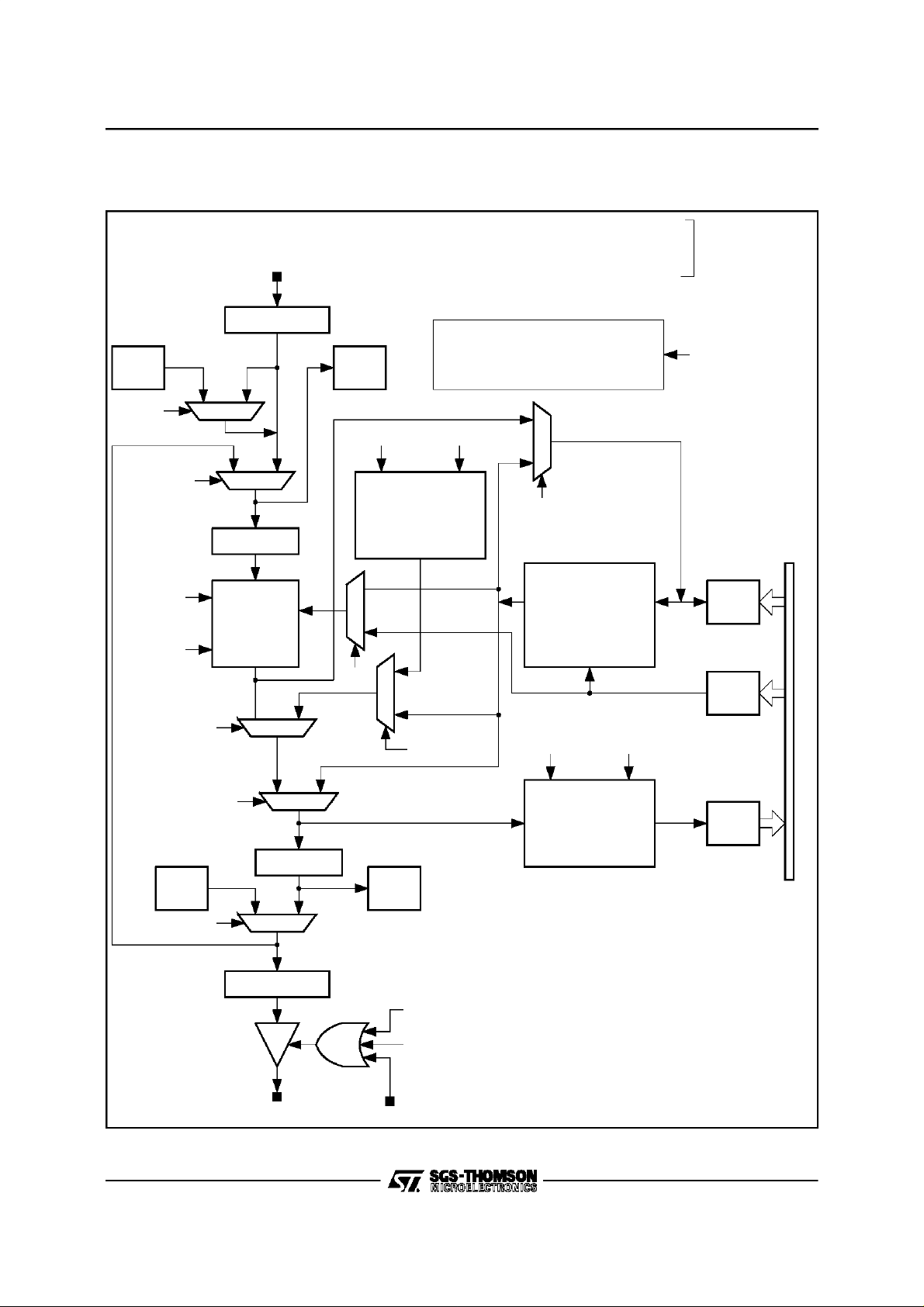
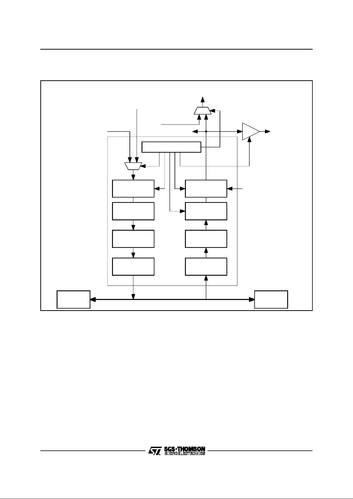
II - BLOCKDIAGRAM
Thetop levelfunctionalities of
Figure1 : GeneralBlock Diagram
DIN5
DIN4
DIN3
25 24 23 22 21 20
GCI1
GCI0
DIN6
26
DIN7
27
DIN8
28
VCX IN
7
8
2
3
4
COUNTER
XTAL
WATCHDOG
32 Rx HDLC
with Adress
Recognition
32 Rx DMAC
VCX OUT
XTAL1
XTAL2
WDO
Multi-HDLC
DIN2
DIN1
DIN0
D7
V10
TIME SLOT ASSIGNER FOR MULTIHDLC
16 Rx
appearon the general block diagram.
0
SWITCHING MATRIX
1
n x64 kb/s
2
3
4
5
6
Pseudo
Random
Sequence
7
Analyser
GCI CHANNELDEFINITION
C/I
16 Rx
MON
Sequence
Generator
16 Tx
Pseudo
Random
C/I
NDIS
39 31 32 33 34
0
1
2
3
4
5
6
7
16 Tx
MON
DOUT0
DOUT1
32 Tx HDLC
with CSMA CR
for Content.Bus
32 Tx DMAC
DOUT2
DOUT3
DOUT4
35
DOUT537DOUT6
36
GCI0
GCI1
Rx
C/IRxMONTxC/ITxMON
INTERRUPT
CONTROLLER
DOUT712FRAME A10CLOCK A13FRAME B11CLOCK B
38
V10
To
Internal
Circuit
CLOCK
SELECTION
18
FSCV*
17
FSCG
9
DCLK
16 FS
5CB
6EC
49 INT0
50 INT1
µP Bus
µP
INTERFACE
Internal Bus
BUS ARBITRATION
Thereare :
- The switching matrix,
- The time slot assigner,
- The 32 HDLC transmitters with associated DMA
controllers,
- The 32 HDLC receivers with associated DMA
controllers,
- The 16 Command/Indicateand MonitorChannel
transmitters belonging to two General Component Interfaces(GCI),
RAM
INTERFACE
RAM
Bus
STLC5464
- The 16 Command/Indicateand Monitor Channel
receivers belonging to two General Component
Interfaces(GCI),
- The memoryinterface,
- The microprocessor interface,
- The bus arbitration,
- The clock selection and time synchronization
function,
- The interruptcontroller,
- The watchdog,
5464-02.EPS
14/83

III - FUNCTIONAL DESCRIPTION
III.1- The SwitchingMatrix N x 64 KBits/S
III.1.1 - Function Description
The matrix performs a non-blockingswitch of 256
time slots from 8 Input Time Division Multiplex
(TDM) at 2 Mbit/sto 8 output Time Division Multiplex.A TDM is composedof 32 TimeSlots (TS)at
64 kbit/s. The matrix is designed to switch a 64
kbit/s channel (Variable delay mode) or an hyperchannel of data (Sequence integrity mode).So, it
will both provide minimum throughput switching
delayfor voiceapplicationsandtimeslotsequence
integrity for data applications on a per channel
basis.
The requirements of theSequence Integrity(n*64
kbit/s)mode are the following:
Allthe time slotsof agiveninputframemust beput
out during a same output frame.
The time slots of an hyperchannel(concatenation
of TS in the same TDM) are not crossed together
at output in different frames.
In variable delay mode, the time slot is put out as
soon as possible. (The delay is two or three time
slots minimum between input and output).
For test facilities, any time slot of an OutputTDM
(OTDM) can be internally looped back into the
sameInput TDM number(ITDM) at thesame time
slotnumber.
A Pseudo Random Sequence Generator and a
Pseudo Random Sequence Analyzer are implemented in thematrix. They allowthe generationa
sequence on a channel or on a hyperchannel,to
analyse it and verify its integrity after several
switching in the matrix or some passing of the
sequenceacross different boards.
The Frame Signal (FS) synchronises ITDM and
OTDMbut a programmabledelay or advancecan
beintroducedseparatelyoneachITDMand OTDM
(a half bit time, a bittime or two bit times).
An additionalpin (PSS) permitsthe generationof
a programmable signal composed of 256 bits per
frameat abit rate of 2048 kbit/s.
STLC5464
An externalpin (NDIS) asserts a high impedance
on all the TDM outputs of the matrix when active
(duringthe initialization of theboard for example).
III.1.2 - Architecture of the Matrix
The matrix is essentially composed of buffer data
memoriesand a connection memory.
Thereceivedserialdatais firstconvertedtoparallel
byaserialto parallelconverterandstoredconsecutively in a 256 position Buffer Data Memory (see
Figure 2 onPage 16).
To satisfy the Sequence Integrity (n*64 kbit/s) requirements,the data memoryis built with an even
memory, an odd memory and an output memory.
Twoconsecutiveframesare storedalternatively in
theoddandevenmemory.Duringthe timeaninput
frame is stored, the one previouslystoredis transferred into the output memory according to the
connectionmemoryswitchingorders.Aframelater,
the outputmemoryis readand datais convertedto
serial and transferred to the outputTDM.
III.1.3 - ConnectionFunction
Twotypes of connectionsare offered:
- unidirectionalconnection and
- bidirectionalconnection.
Anunidirectionalconnectionmakesonlytheswitch
ofaninputtimeslotthroughan outputonewhereas
abidirectionalconnectionestablishesthelinkin the
other direction too. So a doubleconnectioncan be
achieved by a single command (see Figure 3 on
Page 17).
III.1.4 - LoopBack Function
Any time slot of an Output TDM can be internally
looped back on the timeslot which has the same
TDM numberand the same TS number
(OTDMi,TSj) ----> (ITDMi, TSj).
In the case of a bidirectional connection, only the
one specified by the microprocessoris concerned
by the loop back (see Figure 4 onPage 17).
15/83
STLC5464
III - FUNCTIONAL DESCRIPTION(continued)
Figure2 :SwitchingMatrixData Path
D7 DIN’ 0/7 D4/5
Tx
HDLC
HDLCM 1
LOOP
IMTD
Sequence
Integrity
DIN 0/7
BIT SYNCHRO
1
S/P
DATA
MEMORIES
64kb/sand
n x 64kb/s
PRSG : Pseudo RandomSequence Generator
PRSA : PseudoRandom Sequence Analyzer
OTSV : OutputTime Slot Validated
From Connection
Memory
INS : Insert
CM : ConnectionMemory (from CMAR Register)
ME : Message Enable
Rx
GCI
PRSG
PSEUDORANDOM
SEQUENCE
GENERATOR
Rec. O.152
1
A
IMTD : Increased Min Throughtput Delay
SGV : SequenceGenerator Validated
SAV: SequenceAnalyzer Validated
SGV
1
CM
211-1
(whenRead)
CONNECTION
MEMORY
DD
From SMCR Register
Internal
Bus
CMDR
Sequence Integrity,
Data
Register
CMAR
CM
LOOP, PRSA,PRSG,
INS, OTSV
1
D0/7
16/83
Tx
GCI
INS
GCIR
ME
D4/5
1
BIT SYNCHRO
DOUT 0/7
1
P/S
Address
PRSG
1
Rx
HDLC
D7
PRSA
PSEUDORANDOM
SEQUENCE
ANALYZER
Rec. O.152
SAV
211-1
Register
SFDR
SequenceFault
CounterRegister
From Connection Memory
OTSV (per channel)
From OMCR Register
OMV (per multiplex)
From Disable Pin
(for all multiplexes)
5464-03.EPS
III - FUNCTIONAL DESCRIPTION(continued)
Figure3 :Unidirectionaland Bidirectional Connections
STLC5464
Figure4 : LoopBack
OTSy, OTDMq
DOWN STREAM
OTSy, OTDMq
DOWN STREAM
OTSy, OTDMq
DOWN STREAM
ITSy, ITDMq
UP STREAM
DATA
MEMORY
n x 64kb/s
Unidirectional Connection
DATA
MEMORY
n x 64kb/s
DATA
MEMORY
n x 64kb/s
Bidirectional Connection
OTSV
DATA
MEMORY
n x 64kb/s
ITSx,ITDMp
DOWN STREAM
ITSx,ITDMp
DOWN STREAM
OTSx, OTDMp
UP STREAM
DOWN STREAM
p, q = 0 to7
x, y = 0 to 31
ITSx,ITDMp
5464-04.EPS
ITSy, ITDMq
UP STREAM
Loopback per channel relevant if bidirectional connection has been done.
III.1.5 - Delay through the Matrix
III.1.5.1- VariableDelay Mode
In the variable delay mode, the delay through the
matrixdependsontherelativepositionsof theinput
and output time slots in the frame.
So,some limits are fixed:
- the maximumdelay is a frame+ 2time slots,
- the minimum delay is programmable.
Three time slotsifIMTD = 1, inthis case n = 2 in
the fo rmula he reafter or two time slots if
IMTD = 0, in this case n = 1 inthe sameformula
(see Paragraph ”Switching Matrix Configuration
Reg SMCR (0C)H” on Page60).
Allthe possibilitiescan be rankedin three cases :
a) If OTSy> ITSx+ n then the variable delay is :
OTSy- ITSxTime slots
DATA
MEMORY
n x 64kb/s
Loop
OTSx, OTDMp
UP STREAM
p, q = 0 to 7
x, y = 0 to 31
b) IfITSx<OTSy< ITSx+ n thenthevariabledelay
is :
OTSy - ITSx+ 32 Timeslots
c) OTSy < ITSxthenthe variable delay is :
32 - (ITSx- OTSy)Time slots.
N.B. Ruleb) andrule c) are identical.
For n = 1 and n =2, see Figure 5 on Page 18.
III.1.5.2- SequenceIntegrity Mode
In the sequenceintegrity mode (SI = 1, bit located
in theConnectionMemory),theinputtimeslotsare
put out 2 frames later (see Figure 6 on Page 19).
Inthiscase,thedelayis definedbya singleexpression :
ConstantDelay = (32 - ITSx)+ 32 + OTSy
So, the delay in sequence integrity mode varies
from 33 to 95 time slots.
5464-05.EPS
17/83

STLC5464
III - FUNCTIONAL DESCRIPTION(continued)
Figure5 :VariableDelay through the matrixwith ITDM = 1
1) Case : If OTSy > ITSx + 2, then Variable Dela y is : OTSy - ITSx TimeSlots
Frame n Frame n + 1
Inpu t
Frame
Output
Frame
2) Case : If ITSx≤OTSy≤ITSx + 2, then Variable Delay is : OTSy - ITSx + 32 TimeSlots
Inpu t
Frame
Output
Frame
ITS0 ITS31 ITS0 ITS31
OTS0 OTS31
ITS0 ITS31 ITS0 ITS31
OTS0 OTS31
ITSx ITSx+1 ITSx+2
y>x+2
Variable Delay
(OTSy - ITSx)
Frame n Frame n + 1
ITSx ITSx+1 ITSx+2
x≤y≤x+2
OTSy
Variable Delay : OTSy - ITSx + 32 TimeSlots
OTSy
ITSx
32 TimeS lots
OTSy
3) Case : If OTSy < ITSx, then Variable Delay is : 32 - (ITSx - OTSy) Tim eSlots
Frame n Frame n + 1
Inpu t
Frame
Output
Frame
ITS0 ITS31 ITS0 ITS31
OTS0 OTS31
OTSy
ITSx
y<x
Variable Delay : 32 - (ITSx - OTSy) Time Slots
32 TimeSlots
18/83
ITSx
OTSy
5464-06.EPS
III - FUNCTIONAL DESCRIPTION(continued)
Figure6 :VariableDelay through the matrixwith ITDM = 0
1) Case : If OTSy > ITSx + 1, then Variable Delay is : OTSy - ITSx TimeSlots
Frame n Frame n + 1
STLC5464
Input
Frame
Output
Frame
2) Case : If ITSx ≤ OTSy≤ ITSx+ 1, then Variable Delayis : OTSy - ITSx + 32 TimeSlots
Input
Frame
Output
Frame
ITS0 ITS31 ITS0 ITS31
OTS0 OTS31
ITS0 ITS31 ITS0 ITS31
OTS0 OTS31
ITSx ITSx+1 ITSx+2
y>x+1
Variable Delay
(OTSy - ITSx)
ITSx ITSx+1 ITSx+2
x
≤ y ≤ x+1
OTSy
Frame n Frame n + 1
OTSy
Variable Delay : OTSy - ITSx + 32 TimeSlots
32 TimeSlots
ITSx
OTSy
3) Case : If OTSy < ITSx, then Variable Delay is : 32 - (ITSx- OTSy) TimeSlots
Frame n Frame n + 1
Input
Frame
Output
Frame
ITS0 ITS31 ITS0 ITS31
OTS0 OTS31
OTSy
ITSx
y<x
Variable Delay : 32 - (ITSx- OTSy)TimeSlots
32 TimeSlots
ITSx
OTSy
5464-07.EPS
19/83
STLC5464
III - FUNCTIONAL DESCRIPTION(continued)
Figure7 :ConstantDelay through the matrix with SI = 1
Cons tant Delay = (32 -ITSx) + 32 + OTSy
ITS0
ITS :
OTS :
Framen Framen+1 Framen+2
ITS31 ITS0 ITS31 ITS0 ITS31
Min. Constant Delay = 33TS
1+
Input Time Slot
Output TimeSlot
32 TimeSlots + 0 = 33
0≤x≤31
0≤y≤31
OTS0 OTS 31
TimeSlots
20/83
Max. ConstantDelay = 95 TimeSlots
32 - 0 + 32 + 31 = 95
(32 - ITSx)
+32 +OTSy =Constant
OTS 31
TimeSlots
Delay
5464-08.EPS
III - FUNCTIONAL DESCRIPTION(continued)
III.1.6 - ConnectionMemory
III.1.6.1- Description
Theconnection memoryis composedof 256 locations addressed by the numberof OTDM and TS
(8x32).
Eachlocation permits :
- toconnecteachinputtimeslotto one outputtime
slot (If two or more output time slots are connected to the same input time slot number,there
is broadcasting).
- toselectthe variabledelaymodeorthesequence
integritymode for anytime slot.
- to loop back an outputtime slot.In thiscase the
contentsof aninputtimeslot(ITSx,ITDMp)is the
same as the output time slot (OTSx,OTDMp).
- to output the contents of the corresponding connection memory instead of the data which has
been stored in data memory.
- to output the sequence of the pseudo random
sequence generator on an output time slot: a
pseudo random sequencecan be insertedin one
or severaltime slots (hyperchannel)of thesame
Output TDM; this insertion must be enabled by
the microprocessor in the configuration register
of the matrix.
- todefinethe sourceof a sequenceby the pseudo
random sequence analyzer: a pseudo random
sequence can be extracted from one or several
time slots (hyperchannel)of thesame InputTDM
and routedto the analyzer;this extractioncanbe
enabled by the microprocessorin the configuration register of the matrix (SMCR).
- to assert a high impedance level on an output
time slot (disconnection).
- todelivera programmable256-bit sequenceduring 125microsecondsontheProgrammablesynchronizationSignal pin (PSS).
STLC5464
- ConnectionMemoryAddressRegister (CMAR).
III.2 - HDLC Controller
III.2.1 - FunctionDescription
The internal HDLC controller can run up to 32
channels in a conventional HDLC mode or in a
transparent (non-HDLC) mode (configurable per
channel).
Eachchannel bitrateis programmablefrom4kbit/s
to 64kbit/s.All the configurationsare alsopossible
from 32 channels (from 4 to 64 kbit/s) to one
channelat 2 Mbit/s.
Inreception,theHDLCtime slotscandirectlycome
from the input TDM DIN8 (direct HDLC Input) or
from any otherTDM inputafter switching towards
the output 7 of the matrix (configurable per time
slot).
In transmission,the HDLC frames are sent on the
output DOUT6 and on theoutput CB (with or without contention mechanism), or are switched towards the other TDM output via the input 7 of the
matrix (see Figure 8 on Page 22 and Paragraph
III.2.2on Page23).
III.2.1.1- Formatof the HDLC Frame
Theformatof anHDLCframeisthesameinreceive
and transmitdirectionand shownhere after.
III.2.1.2- Composition of an HDLC Frame
Opening Flag
Address Field (first byte)
Address Field (second byte)
Command Field (first byte)
Command Field (second byte)
Data (first byte)
III.1.6.2- Access to ConnectionMemory
Supposingthat theSwitchingMatrix Configuration
Register(SMCR) has been already written by the
microprocessor, it is possibleto accessto the connectionmemoryfrom microprocessor with the help
of two registers :
- ConnectionMemory Data Register(CMDR) and
- ConnectionMemory Address Register (CMAR).
III.1.6.3- Access to Data Memory
To extract the contents of the data memory it is
possibleto readthe data memory from microprocessorwith the help of the two registers :
- ConnectionMemory Data Register(CMDR) and
Data (optional)
Data (last byte)
FCS (first byte)
FCS (second byte)
Closing Flag
- OpeningFlag
- One or two bytes for address recognition(reception) and insertion(transmission)
- Data bytes with bit stuffing
- Frame Check Sequence: CRC with polynomial
G(x) = x16 +x12+x5+1
- ClosingFlag.
21/83
STLC5464
III - FUNCTIONAL DESCRIPTION(continued)
Figure8 :HDLC and DMAControllerBlock Diagram
From Output 7
of the Matrix
From Output 6
of the Matrix
Direct HDLC Input
DIN 8
To Input 7 ofthe Matrix
TIME SLOT AS SIGNER
DOUT 6
Direct HDLC Output
Contention
Bus
P
µ
INTERFACE
32 Rx HDLC
32 ADDRES S
RECOGNITION
32 Rx FIFO’s
32 Rx DMAC 32 Rx DMAC
32 CSMA-CR
32 Tx HDLC
32 Tx FIFO’s
Echo
RAM
INTERFACE
5464-09.EPS
22/83

III - FUNCTIONAL DESCRIPTION(continued)
III.2.1.3- Descriptionand Functions of the
HDLCBytes
- FLAG
The binarysequence01111110marks thebeginning and the end of the HDLCFrame.
Note : In reception,three possibleflag configurations are allowed and correctlydetected :
- two normal consecutiveflags :
...0111111001111110...
- two consecutiveflags with a ”0” common :
...011111101111110...
- a global common flag : ...01111110...
this flag is the closing flag for the current frame
and theopening flagfor the nextframe
- ABORT
The binary sequence 1111111 marks an Abort
command.
Inreception,sevenconsecutive1’s,insidea message, are detected as an abort command and
generatesan interrupt to the host.
In transmit direction, an abort is sent upon command of the micro-processor. No ending flag is
expected after the abort command.
- BITSTUFFING AND UNSTUFFING
This operation is done to avoid the confusion of
a databyte with a flag.
In transmission, if fiveconsecutive1’s appear in
theserialstreambeingtransmitted,azero isautomaticallyinserted(bit stuffing)after hefifth ”1”.
In reception, if fiveconsecutive”1” followed by a
zero are received, the ”0” is assumed to have
been inserted and is automatically deleted (bit
unstuffing).
- FRAMECHECK SEQUENCE
TheFrameCheckSequenceiscalculatedaccordi ng
totherecommendationQ921oftheCCITT.
- ADDRESS RECOGNITION
In the frame, one or two bytes are transmittedto
indicate the destinationof the message.
Two types of addressesare possible :
- a specific destinationaddress
- a broadcast address.
In reception, the controller compares the receive
addressesto internalregisters,whichcontainthe
addressmessage.4bitsinthe receivecommand
register (HRCR) inform the receiver of which
registers,it hasto takeinto accountfor the comparison.The receiver compares thetwo address
bytes of the message to the specific board address and the broadcast address. Upon an address match, the address and the datafollowing
are writtento the data buffers;upon an address
mismatch,the frame is ignored.So, it authorizes
the filteringof the messages.Ifno comparisonis
STLC5464
specified, each frame is received whatever its
addressfield.
In Transmission, the controller sends the frame including the destinati on or broadcastaddresses .
III.2.2 - CSMA/CRCapability
An HDLC channel can come in and goout by any
TDM input on the matrix. For time constraints,
direct HDLC Accessis achievedby the input TDM
(DIN 8) and theoutputTDM (DOUT6).
Intransmission,a timeslotofaTDMcanbe shared
between different sources in Multi-point to point
configuration(differentsubscriber’s boards for example). The arbitration system is the CSMA/CR
(Carrier Sense Multiple access with Contention
Resolution).
The contention is resolved by a bus connectedto
the CB pin (ContentionBus).This bus is a 2Mbit/s
wire line commonto allthe potentialsources.
Multi-HDLC
If a
thedatato transmitis sentsimultaneouslyontheCB
lineandtheoutputTDM. Theresultofthe contention
isreadbackontheEcholine.Ifacollisionisdetected,
the transmission is stoppedimmediately. Acontentionona bitbasisisso achieved. Each message to
be sentwithCSMA/CRhas a priorityclass(PRI= 8,
10) indicatedby theTransmit Descriptor and some
rulesare implementedto arbitratethe accessto the
line. The CSMA/CR Algorithm is given. When a
requestto send a message occurs, the transmitterdetermines if thesharedchannelisfree.The
Multi-HDLC
consecutive ”1” are detected (C dependingon the
message’spriority), the
its message. Each bit sent is sampled back and
compared with the original value to send. If a bit is
different, the transmission is instantaneously
stopped (before the end of this bit time) and will
restartas soonasthe
channel is freewithout interruptingthe microprocessor.
After a successful transmission of a message, a
programmablepenaltyPEN(1or2) isappliedtothe
transmitter (see ParagraphHDLC Transmit CommandRegisteron Page65).It guaranteesthat the
same transmitterwill nottakethe busanothertime
before a transmitterwhich has to send a message
of same priority.
In case of a collision, the frame which has been
abortedis automaticallyretransmittedby theDMA
controller without warning the microprocessor of
this collision. The frame can be located in several
buffers in external memory. The collision can be
detectedfrom the second bit of theopeningframe
to thelast but one bitof the closingframe.
hasobtained the accessto the bus,
listens to the Echo line. If C or more
Multi-HDLC
Multi-HDLC
beginsto send
willdetectthatthe
23/83

STLC5464
III - FUNCTIONAL DESCRIPTION(continued)
III.2.3 - TimeSlot AssignerMemory
Each HDLC channel is bidirectional and configurateby the Time Slot Assigner(TSA).
TheTSAis amemoryof 32 words(oneper physical
TimeSlot)whereall ofthe 32inputand outputtime
slots of the HDLC controllerscan be associated
to logical HDLC channels. Super channels are
created by assigning the same logical channel
numberto severalphysicaltime slots.
The following features are configurate for each
HDLC time slot :
- Time slot used or not
- Onelogicalchannel number
- Itssource : (DIN 8 or theoutput 7 of thematrix)
- Its bit rate and concerned bits (4kbit/s to
64kbit/s). 4kbit/s correspondto one bit transmitted each two frames. This bit mustbe present in
two consecutive frames in reception, and repeated twice in transmission.
- Itsdestination :
- direct output on DOUT6
- direct output on DOUT6and on the Contention
Bus(CB)
- on another OTDM via input7 of the matrix and
on theContentionBus (CB)
III.2.4 - Data Storage Structure
Dataassociatedwitheach Rx andTx HDLCchannelisstoredinexternalmemory;Thedatatransfers
between the HDLC controllers and memory are
ensuredby32 DMAC(DirectMemoryAccessController)in receptionand 32 DMAC in transmission.
The storage structure chosen in both directionsis
composed of one circular queue of buffers per
channel. In such a queue, each data buffer is
pointedto by a Descriptorlocatedinexternalmemory too. The main information contained in the
Descriptor is the address of the Data Buffer, its
length and the address of the next Descriptor; so
the descriptors can belinked together.
This structure allows to :
- Store receive frames of variable and unknown
length
- Readtransmitframes stored in external memory
by thehost
- Easilyperform the frame relay function.
III.2.4.1- Reception
At the initialization of the application, the host has
to prepare an Initialization Block memory, which
containsthe firstreceive buffer descriptoraddress
for eachchannel, and the receivecircularqueues.
At the opening of a receive channel, the DMA
controller reads the address of the first buffer descriptorcorrespondingtothischannelin the initialization Block. Then, the data transfer can occur
withoutinterventionof the processor(see Figure 9
on Page 25).
Anew HDLCframe always begins in a new buffer.
A long frame can be splitbetween severalbuffers
if thebuffersize is not sufficient.All the information
concerning the frame and its location in the
circular queue is included in the Receive Buffer
Descriptor:
- The ReceiveBufferAddress(RBA),
- The size of thereceive buffer (SOB),
- Thenumberof byteswrittenintothebuffer(NBR),
- The NextReceive DescriptorAddress (NRDA),
- The status concerningthe receive frame,
- The controlof the queue.
III.2.4.2- Transmission
In transmission, the data is managed by a similar
structure as in reception (see Figure 10 on
Page 25).
By thesame way, a frame can be split up between
consecutivetransmit buffers.
The main information contained in the Transmit
Descriptorare :
- transmitbufferaddress (TBA),
- numberof bytesto transmit(NBT)concerningthe
buffer,
- next transmit descriptoraddress (NTDA),
- statusof theframe after transmission,
- control bit of the queue,
- CSMA/CRpriority(8 or10).
III.2.4.3- FrameRelay
The principle of the frame relay is to transmit a
frame which has been received without treatment.
A new heading is just added. This will be easily
achieved,takingintoaccountthat the queue structure allows the transmission of a frame split between several buffers.
24/83

III - FUNCTIONAL DESCRIPTION(continued)
Figure9 :Structureof the Receive Circular Queue
Initialization Block
up to 32 channels
RDA0
RDA1
RDA31
Initial Receive
Descriptor
NRDA
RBA
RECEIVE
DMA
CONTROLLER
Receive
Descriptor 2
NRDA
RBA
STLC5464
Receive
Buffer 1
Receive
Descriptorn
NRDA
RBA
Receive
Buffer n
One receive circular queue by channel
Figure10 : Structureof the TransmitCircular Queue
Initialization Block
up to 32 channels
TDA0
TDA1
TDA31
Initial Transmit
Descriptor
NTDA
TBA
Receive
Buffer 3
TRANSMIT
DMA
CONTROLLER
Receive
Buffer 2
Receive
Descriptor3
NRDA
RBA
Transmit
Descriptor 2
NTDA
TBA
5464-10.EPS
NTDA
TBA
Transmit
Descriptor n
Transmit
Buffer n
Transmit
Buffer 1
Transmit
Buffer 3
One transmit circular queue by channel
Transmit
Buffer 2
Transmit
Descriptor3
NTDA
TBA
5464-11.EPS
25/83
 Loading...