

QUAD LINE FEED CONTROLLER
■ BATTERY VOLTAGE UP TO 120V
■ SUPPLIES POWE R FOR UP TO FOUR
DIGITAL TELEPHONE LINES
■ PROGRAMMABLE CURRENT LIMITING
■ LONGITUDINAL CURRENT CANCELLATION
■ ETSI ETR80 COMPL IAN T
■ OUTPUT CURRENT UP TO 140 mA
■ STATUS CONDITION DETECTION FOR
EACH LINE
■ AUTOMATIC THERMAL PROTECTION
■ AUTO POWER ON SEQUENCE
■ OUTPUT STAGE OPTIMIZED FOR MINIMAL
OUTPUT OVERVOLTAGE PROTECTION
■ TWO EXTERNAL RELAY DRIVERS PER LINE
■ PARALLEL OR MPI CONTROL INTERFACE
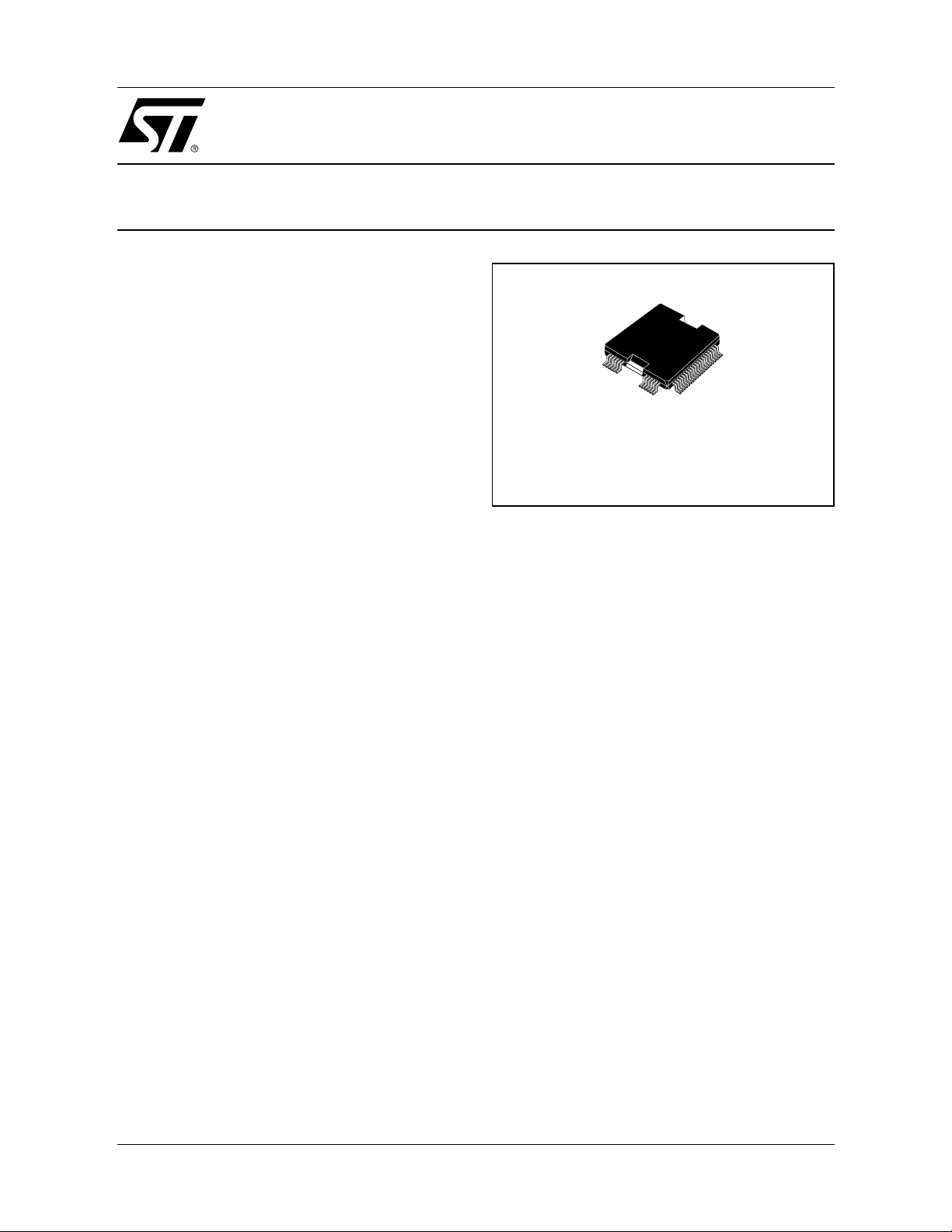
■ HI-QUAD PACKAGE 64 PIN
DESCRIPTION
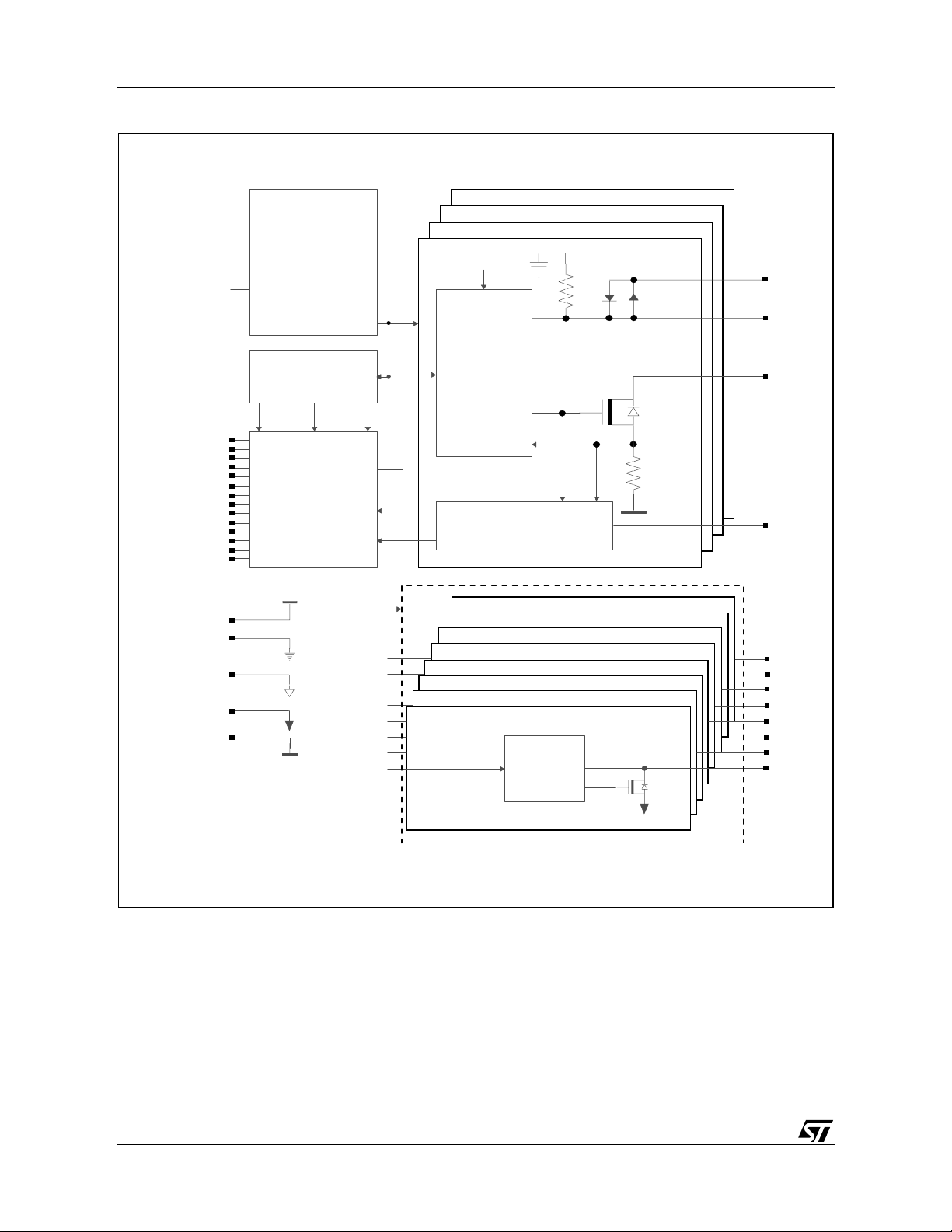
The QUAD LINE FEED CONTROLLER provides a
power source for up to four U line interfaces. The
power source to the device is a local battery or a centralized regulated power supply. Each powered line is
individually controll ed and monitored by the device
interface.
A MPI or a simple parallel interface can be selected
STLC5445
HiQUAD-64
ORDERING NUM BER: STLC 5445
by a pin strap.
Each line can be individually powered and monitored:
therefore overload and faults can easi ly be detected
and localized even in a large system. The status conditions detected by the device are: Current Overload,
Thermal Overload, Open Loop. If activated (by
means of a dedicated pin strap), a self generated
power on sequence avoids the thermal over stress
when a simultaneous power on has been r equested
for more than one channel. The current limiting value
can globally be programmed for the four channels by
means of an external resistor. The device has two integrated relay drivers per line to drive the test relays
of the ISDN system.
October 2002
1/23
STLC5445
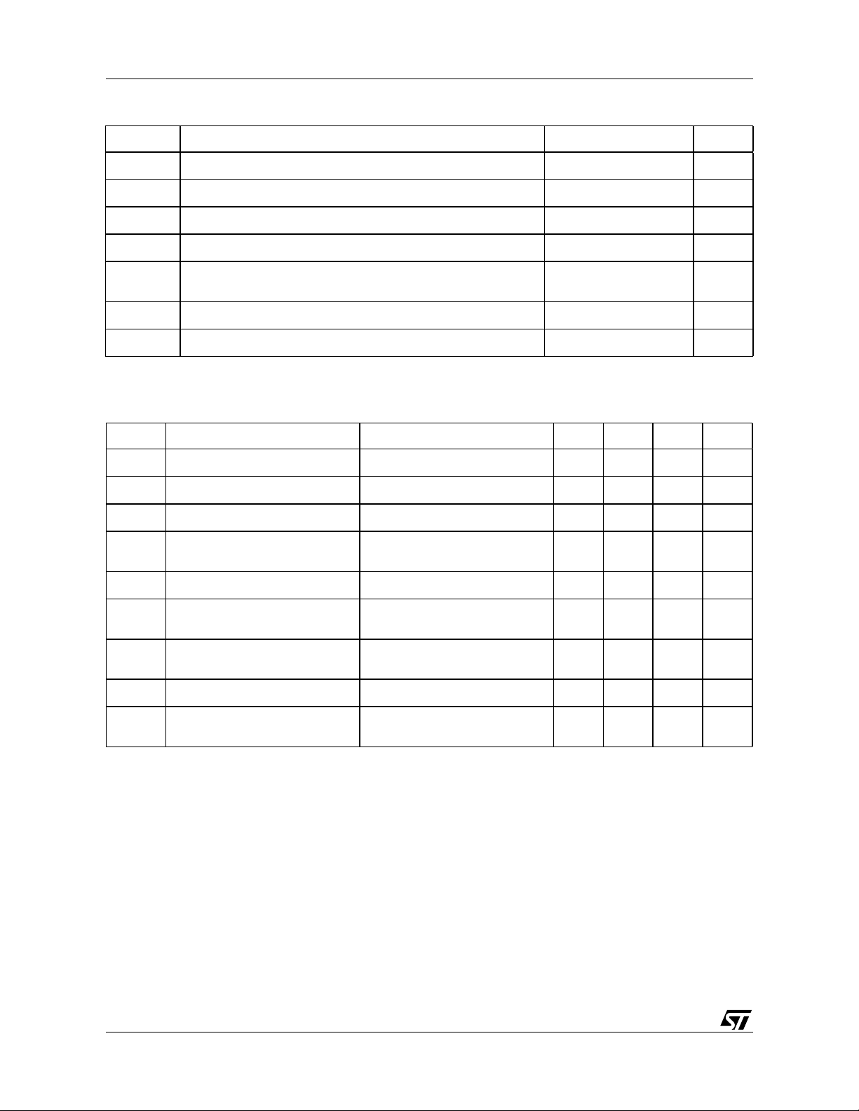
BLOCK DIAGRAM
ILIM
110°C
PSC
PBIT
CKILC
RESETN
INTN
ALE
ES0 (A0)
ES1 (CSN)
ES2 (RDN)
ES3 (WRN)
NACK0 (D0)
NACK1 (D1)
NACK2 (D2)
NACK3 (D3)
Reference & biasing
generation
Thermal
monitoring
130°C
160°C
Logic
interface
Limiting
current
reference
Voltage
and
current
biasing
COD
OLD
Channel 3
Channel 2
Channe l 1
Channel 0
On / Off
&
line current
control
COD & OLD
generation
WBP0
WB0
WA0
V
BAT
CODC0
V
CC
VCC
BGND
EREL3B
DGND
EREL3A
EREL2B
RGND
VBAT
V
BAT
EREL2A
EREL1B
EREL1A
EREL0B
EREL0A
I / O conne ctions on channels 1, 2 and
3 are similar to those
shown for channel 0 but have been omitted for clarity
reasons.
Relay driver 3B
Relay driver 3A
Relay driver 2B
Relay driver 2A
Relay driver 1B
Relay driver 1A
Relay driver 0B
Relay driver 0A
Driving
&
output
clamping
REL3B
REL3A
REL2B
REL2A
REL1B
REL1A
REL0B
REL0A
2/23
STLC5445
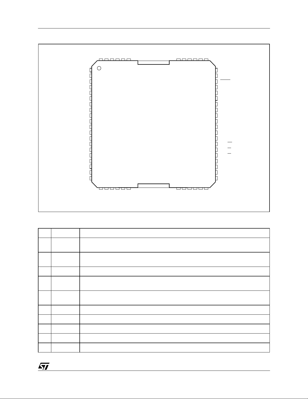
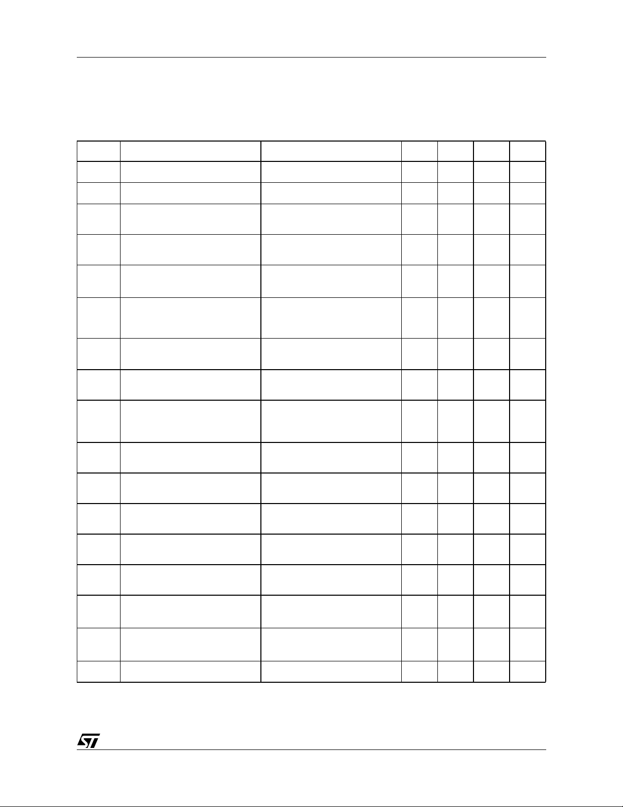
PIN CONNECTION
NACK0(D0)
NACK1(D1)
*EREL0A
*EREL0B
*EREL1A
*EREL1B
(Top view)
CODC0
CODC1
RGND
CK_ILC
REL0A
REL0B
REL1A
REL1B
ALE
PBIT
PSC
INTN
BGND
N.C.
WA0
BGND
63
64
1
2
3
4
5
6
7
8
9
10
12
13
14
15
16
17
18
19
20
21 22 23 24 25
62
VBAT
WB0
WBP0
RGND
60
61
59 58 57 56 55 54 53
26
VBAT
WB3
WBP3
ILIM
N.C.
271128 29 30 31 32
WA3
52
51
50
49
48
47
46
45
44
43
42
41
40
39
38
37
36
35
34
33
N.C.
BGND
*RESET
NACK3(D3)
NACK2(D2)
REL3B
*EREL3B
*EREL3A
REL3A
REL2B
*EREL2B
*EREL2A
REL2A
*ES3(WR)
*ES2(RD)
*ES1(CS)
*ES0(A0)
RGND
CODC3
CODC2
CC
V
N.C.
WA1
*INTERNAL PULL DOWN TO GROUND
WBP1
WB1
VBAT
VBAT
WB2
WBP2
DGND
WA2
BGND
D99TL437
PIN FUNCTION
N° Pin Name Description
1 CODC0 Pin for connection of the external capacitor (100nF/6.3V) to GND for COD signal filtering on
channel 0.
2 CODC1 Pin for connection of the external capacitor (100nF/6.3V) to GND for COD signal filtering on
channel 1
4 CKILC External clock input pin for the internal power on sequencer
5 NACK0(D0) Logic pin: with PSC = 0, Line 0 status information output
6 NACK1(D1) Logic pin: with PSC = 0, Line 1 status information output
7 REL0A Output of the 0A relay driver
8 *EREL0A Logic input pin: relay 0A output driver’s ON/OFF (high = ON)
9 *EREL0B Logic input pin: relay 0B output driver’s ON/OFF (high = ON)
10 REL0B Output of the 0B relay driver
with PSC = 1, Line 0 I/O tristate data bus
with PSC = 1, Line 1 I/O tristate data bus
11 REL1A Output of the 1A relay driver
3/23
STLC5445
PIN FUNCTION
N° Pin Name Description
12 *EREL1A Logic input pin: relay 1A output driver’s ON/OFF (high = ON)
13 *EREL1B Logic input pin: relay 1B output driver’s ON/OFF (high = ON)
14 REL1B Output of the 1B relay driver
15 ALE Logic input pin: with PSC = 0, Don’t care
16 PBIT Power on sequencer enable: PBIT = 0: power on sequencer ON
17 PSC Parallel or MPI mode input selection pin:
18 INTN Logic output pin; open drain: with PSC = 0 high impedance
21 WA1 Output feeder’s switch side of line 1; negative respect to WB1
23 VCC Positive supply voltage. It is referred to DGND
24 WBP1 Internal protection diodes for line 1
25 WB1 Output feeder’s resistive side of line 1; positive respect to WA1
28 WB2 Output feeder’s resistive side of line 2; positive respect to WA2
(continued)
with PSC = 1, Address Latch Enable (active high)
PBIT = 1: power on sequencer OFF
0 = parallel interface; 1 = MPI interface
with PSC = 1 interrupt (active low)
29 WBP2 Internal protection diodes for line 2
30 DGND Digital ground
31 WA2 Output feeder’s switch side of line 2; negative respect to WB2
33 CODC2 Pin for connection of the external capacitor (100nF/6.3V) to GND for COD signal filtering on
channel 2
34 CODC3 Pin for connection of the external capacitor (100nF/6.3V) to GND for COD signal filtering on
channel 3
36 *ES0(A0) Logic input pin: with PSC = 0, Line 0 ON/OFF request (high=ON)
37 *ES1(CSN) Logic input pin: with PSC = 0, Line 1 ON/OFF request (high=ON)
38 *ES2(RDN) Logic input pin: with PSC = 0, Line 2 ON/OFF request (high=ON)
39 *ES3(WRN) Logic input pin: with PSC = 0, Line 3 ON/OFF request (high=ON)
40 REL2A Output of the 2A relay driver
41 *EREL2A Logic input pin: relay 2A output driver’s ON/OFF (high = ON)
42 *ERL2B Logic input pin: relay 2B output driver’s ON/OFF (high = ON)
43 REL2B Output of the 2B relay driver
with PSC = 1, Address bit for R/W operations
with PSC = 1, chip select (active low)
with PSC = 1, Read command (active low)
with PSC = 1, Write command (active low)
44 REL3A Output of the 3A relay driver
4/23
STLC5445
PIN FUNCTION
N° Pin Name Description
45 *EREL3A Logic input pin: relay 3A output driver’s ON/OFF (high = ON)
46 *ERL3B Logic input pin: relay 3B output driver’s ON/OFF (high = ON)
47 REL3B Output of the 3B relay driver
48 NACK2 (D2) Logic pin: with PSC = 0, Line 2 status information output
49 NACK3 (D3) Logic pin: with PSC = 0 line 3 status information output
50 *RESETN Logic input pin: reset (active low)
53 WA3 Output feeder’s switch side of line 3; negative respect toWB3
55 ILIM Current limit programming input
56 WBP3 Internal protection diodes for line 3
57 WB3 Output feeder’s resistive side of line 3; positive respect to WA3
60 WB0 Output feeder’s resistive side of line 0; positive respect to WA0
61 WBP0 Internal protection diodes for line 0
0 WA0 Output feeder’s switch side of line 0; negative respect to WB0
(continued)
with PSC = 1, Line 2 I/O tristate data bus
with PSC = 1 line 3 I/O tristate data bus
26
27
58
59
19
32
51
64
3
35
62
* Internal pull down to ground
VBAT Negative battery supply voltage. It is referred to BGND
BGND Battery ground
RGND Relay ground
5/23
STLC5445
ABSOLUTE MAXIMUM RATINGS
Symbol Parameter Value Unit
V
V
V
V
I
WBn
I
NEG
T
DD
CD
BB
BD
stg
Voltage from digital input to DGND – 0.5 to VCC + 0.5 V
Voltage from VCC to DGND – 0.4 to +7 V
Voltage from VBAT to BGND – 143 to + 0.4 V
Voltage from BGND to DGND – 3 to +0.5 V
AC Current into the WBn outputs
(WBPn not connected to GND
250 mA
peak
Negative current injected in the WAn outputs (-40 to +85°C) 50 mA
Storage temperature – 60 to 150 °C
RECOMMENDED OPERATING CONDITION
Symbol Parameter Test Condition Min. Typ. Max. Unit
VCC supply voltage 4.75 5.25 V
CC
V
BAT
supply voltage – 120 – 38 V
BAT
BGND/DGND voltage – 3 0.5 V
(1)
Programmable range of the
current limiting function
20 140 mA
V
V
I
LIMT
V
BGND
I
Relay
T
a normal
Relay driver current 70 mA
Ambient temperature normal
range
T
a extend ed
Ambient temperature extended
range
Max operating loop current 140 mA
External, short circuit resistive
MIN
R
I
loop
load from WAn to WBn
070°C
– 40 85 °C
55 W
6/23
STLC5445
ELECTRICAL CHARACTERISTCS
Unless otherwise specified the below listed parameters' values are referred to the following conditions:
V
= –115V, VCC = 5V, R
BAT
range [0°C to 70°C]. The presence of an asterisk mark (*) indicates that the marked parameter must remain
within the specified tolerance in the extended temperature range [-40°C to 85°C].
Symbol Parameter Test Condition Min. Typ. Max. Unit
= 53.6 kW, CODCn RC series = 100nF ±10% and 510Ω ±1%, normal temperature
lim
I
I
VBAT
I
LIMT
I
LIMTL
I
LIM%
R
R
∆R
T
Vcc
I
HZ
WA
WB
j110
VCC supply current All the switches on Νo load 2.5 mA
V
supply current All the switches on Νo load 1.5 1.8 mA
BAT
Current limiting value with
I
= 0 42.5 50 57.5 mA
long
transversal line current only
Current limiting value with added
See Fig.1 37.5 50 62.5 mA
longitudinal line current
Current limiting accuracy in the
range 20 to 140 mA
(1)
I
= 0 ±15 %
long
Leakage current of each WAn
output to ground with output
driver disabled
Resistance from WAn to
V
BAT
Resistance from WBn to
IWA = 30mA 3.15 5.5 7.85 Ω
IWB = 30mA 3.5 5.5 7.5 Ω
BGND
Absolute value of the difference
OUT
between R
R
WBn
and its related
WAn
110°C thermal monitoring
IWA = IWB = =30mA 0.7
110 °C
threshold
50* µA
Ω
1(*)
LV
V
V
I
T
j130
T
j160
T
hyst
out
Rel33
Rel70
Rleak
130°C thermal monitoring
130 °C
threshold
160°C thermal monitoring
160 °C
threshold
Thermal monitoring
10 °C
hysteresis
(2)
Longitudinal output component of
See Fig. 2 – 60 dBV
the fCKILC clock signal
Relay drivers’ output voltage All the relay drivers activated at a
load current of 33mA.
(3)
Relay drivers output voltage All the relay drivers activated at a
load current of 70mA.
(3)
Relay driver leakage current ERLn = Low 100 µA
0.5 V
1.2 V
7/23
 Loading...