

QUAD FEEDER POWERSUPPLY
SUPPLIES POWER FOR UP TO FOUR DIGITAL TELEPHONELINES
CONFORMS TO THE CCITT RECOMMENDATIONS FOR POWER FEED AT THE S OR
T REFERENCE POINTS
SUPPORTS POINT-TO-POINT AND POINT
TO MULTIPOINTCONFIGURATIONS
EACH OF THE FOUR LINES IS INDIVIDUALLY CONTROLLED
HIGH-VOLTAGE BCD TECHNOLOGY SUPPORTING UPTO -130V
AUTOMATIC THERMALSHUTDOWN
STATUS CONDITION DETECTION (BY MI-
CROPROCESSOR) FOR EACHLINE:
– Lowoutput voltage
– Openloop
– Currentoverload
– Thermaloverload
– Normalline condition
PROGRAMMABLECURRENT LIMITING
OUTPUTCURRENT UP TO 120mA
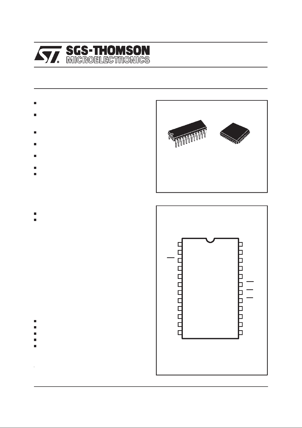
STLC5444
DIP24 PLCC44
ORDERING NUMBERS: STLC5444B1 (DIP24)
STLC5444FN (PLCC44)
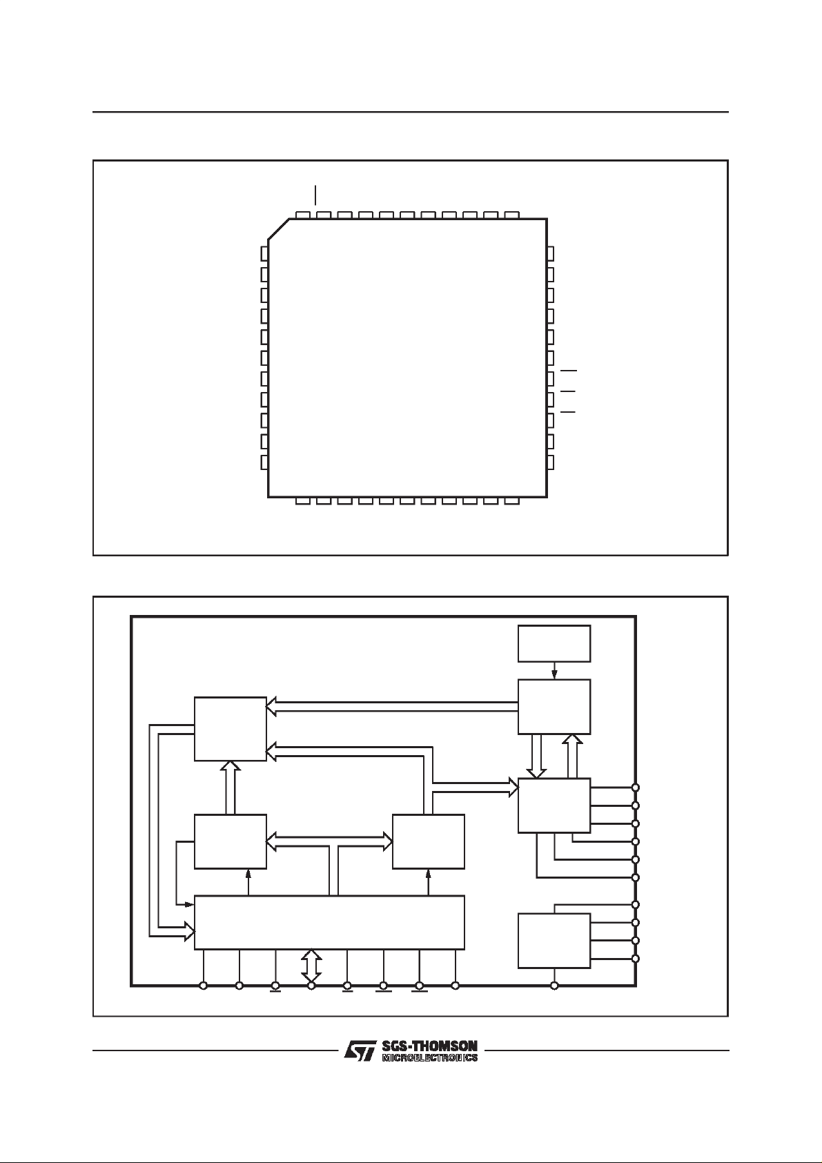
DIP24 PINCONNECTION (Top view)
DESCRIPTION
The ISDN Quad Feeder Power Supply (IQFPS)
provides a power source for up to four line interfaces. The power source to the device is a local
battery or a centralizedregulatedpower supply.
It can operate in point-to-point and point-to-multipoint configurations as far as S interface is concerned.
By the device microprocessor interface, each
powered line is individually controlled and monitored.
Therefore,overloads and faultsare easy to detect
and localizeeven in a large system.
The status conditions detected by the device on
each line that may be read by the microprocessor
are :
low output voltage
openloop
currentoverload
thermaloverload
normalline conditions
A hardware currentlimiting programmable feature
is available.
D1
D0
INT
BGND
VCC ALE
ILIM
N.C.
VBB
N.C.
S0
S1
VBB
1
2
3
4
5
6
7
8
9
10
11
12
D94TL102
24
23
22
21
20
18
17
16
15
14
13
D2
D3
A0
DGND
WR19
CS
RD
RESET
S3
RSRVD
S2
December 1997
1/17
STLC5444
PLCC44 PIN CONNECTION (Top view)
VBB
INT
N.C.
D0
N.C.
D1
N.C.
D2
D3
A0
VBB
BLOCK DIAGRAM
VBB
N.C.
BGND
N.C.
VCC
ILIM
N.C.
N.C.
VBB
N.C.
VBB
7
8
9
10
11
12
13
14
15
16
17
N.C.
S0
N.C.
S1
123564
2322211918 20 28272624 25
N.C.
VBB
S2
N.C.
N.C.
S3
40414244 43
39
38
37
36
35
34
33
32
31
30
29
N.C.
VBB
N.C.
N.C.
DGND
ALE
N.C.
WR
CS
RD
RESET
VBB
D94TL103
2/17
BIT 3
OUTPUT
BUS D3/D0
THERMAL
OVERLOAD
STATUS GROUP BUS
MUX
ADDRESS
INDIRECT
ADDRESS
REGISTER
INT EN
ALE A0 CS D3/D0 RD WR INT RESET ILIM
LINE ENABLE REGISTER BUS
BUS 0/2
INPUT BUS D3/D0
IAR EN
µP
INTERFACE
S DRIVERS
DISABLE
O/3
LINE
ENABLE
REGISTER
LER EN
STATUS
DETECTOR
S
DRIVERS
VOLTAGE
REFERENCE
LINE
STATUS
BUS
S0
S1
S2
S3
VBB(12)
BGND
DGND
VCC
VBB(8)
D94TL104B
PIN DESCRIPTION
o
Name
D1 1 1 Bit 1 of the tri state I/O data bus
NC 2,4,8,10,
D0 3 2 Bit 0 of the tri state I/O data bus
INT 5 3 Active low interrupt output for the µP (open drain)
VBB 6,7
BGND 9 4 Battery ground line
VCC 11 5 +5V supply line
ILIM 12 6 Current limit programming
S0 19 10 Output of the power switch controller 0
S1 21 11 Output of the power switch controller 1
S2 24 13 Output of the power switch controller 2
RSRVD – 14 Reserved pin:it must be left floating
S3 27 15 Output of the power switch controller 3
RESET 30 16 Active high reset input
RD 31 17 Active low read input
CS 32 18 Active low chip select input
WR 33 19 Active low write input
ALE 35 20 Active high address latch enable
DGND 36 21 Digital ground
A0 41 22 Address bit for R/W operations on the data bus
D3 42 23 Bit 3of the I/O tristate data bus
D2 43 24 Bit 2of the I/O tristate data bus
N
PLCC
13,14,
16,18,
20,23,
25,26,
28,34,
37,38,44
15,17
22,29,
39,40
o
N
DIP
7,9 No connection
8,12 Battery supply line (negative battery‘s terminal)
STLC5444
Function
FUNCTIONAL DESCRIPTION
ADDRESS LINE(Input)
A0 selects source and destination locations for
read and write operations on the data bus. A0
must be valid on the falling edge of ALE or during
RD and WR if ALE istied High.
ALE - Address Latch Enable (Input; Active
High)
ALE is an input control pulse used to strobe the
address on the A0 line into the address latch.
This signal is active High to admit the input address. The address is latched on the High-Low
transition of ALE. While ALE is High, the address
latch is transparent. For an unmultiplexed microprocessorbus, ALEmust be tiedHigh.
BGND - GroundBattery
CS - Chip Select(Input; Active Low)
CS must be Low to enable the read or write operations of the device. Data transfer occurs over
the D3-D0 lines.
D3-D0 - DATA BUS (Input/Output; Three-State)
The four bidirectional data bus lines are to exchange information with a microprocessor. D0 is
the least significant bit and D3 is the most significant bit. A High on the data bus corresponds to a
logical 1. These lines act as input when WR and
CS are active and as output when RD and CS are
active. When CS is inactive, the D3-D0 pins are
placed in a high-impedancestate.
3/17

STLC5444
FUNCTIONAL DESCRIPTION (continued)
DGND - Ground Digital
ILIM - Current Limit Programming (Input)
ILIM programs the current limit of the Output drivers using an external resistor connectedbetween
ILIM and VBB. The ILIM pin is 1.25V more positive than VBB. The current limit is 5mA plus 1000
times the current in the external resistor.The programmed currentlimit applies to each driver.
INT - Interrupt (Output; Open-Collector, Active
Low)
INT augments the Microprocessor Interface by
generating an interrupt when a Current Overload
Detector (COD) occurs. INT is active whenever
any bits in the COD register are active. INT is not
latched; when the COD register is zero, INT goes
inactive (High). INT will also go inactive if the
IQFPS automatically disables the S-output driver
that caused the interrupt (due to Thermal Overload), or if the microprocessor disables that line
via the Line Enable Register (LER). COD interrupts can be masked via the Indirect Address
Register (IAR); RESET always disables the INT
pin.
transferredto D3-D0.
RESET- Reset (Input;Active High)
RESET initialize the registers in the device, leaving the driversswitchedoff.
S3-S0 - Drivers(Output)
S3-S0 each supplypower to one line. The outputs
can sink up to 120 mA each. The voltage at the
line is connected to VBBthrough a DMOSswitch.
VBB - BatteryVoltage (input)
VBB is the internal negative supply voltage. VBB
must always be connected to the most negative
supply voltage. The MPI Registers will not function properly when the battery power is disconnected, that is, when VBB is floating or grounded.
The IQFPS should also be reset if a drastic transientis applied to VBB.
VCC - +5VPower Supply(Input)
RD - Read (Input; Active Low)
The active Low read signal is conditioned by CS
and transfers internal information to the data bus.
If A0 is a logical 0, logic levels of the Indirect Address Register (IAR) and Thermal Shutdown
Status bit will be transferred to D3-D0. If A0 is a
logical 1, the data addressed by the IAR will be
WR - Write (Input; Active Low)
The active Low write signal is conditioned by CS
and transfers information from the data bus to an
internal register selected by A0. If A0 is a logical
1, D3-D0 is written into the Line Enable Register
(LER). If A0 is a logical 0, D3-D0 is written into
the IAR. LER and IAR are the only two writable
registersin thedevice.
4/17
STLC5444
DC CHARACTERISTICS (VBB= -54V; VCC= 5V;unlessotherwise specified)
Symbol Parameter Test Conditions Min. Typ. Max. Unit
Input Voltage High Level 2 V
IH
Input Voltage Low Level 0.8 V
IL
High Level Output Current VOH= 2.4V 400 µA
Low Level Output Current VOL= 0.4V 2 mA
High Level Input Current VIH=2V 10 µA
IH
Low Level Input Current VIL= 0.8V 60 µA
IL
Output Hi-Z Current High 2.4V < VOZ<V
CC
Output Hi-Z Current Low 0V < VOZ< 0.4V 10 µA
VCCsupply Current 1.4 5 mA
Logic I/OCapacitance 10 pF
L
Saturation Voltage IS= 80mA 2 V
Output DMOS Saturation Resistivity IS= 80mA 25
on
VBBSupply Current VBB= -54V, R
= 26.6KΩ,
LIM
3.2 6 mA
10 µA
Ω
V
V
V
I
I
I
I
I
OZH
I
OZL
I
C
R
I
OH
OL
CC
SAT
BB
Output Disabled
I
∆
SLIM
Delta Limit Current vs.
Theoretical Programmed Value
I
SLIM
R
= 26.6KΩ,VBB= -96V
LIM
R
= 10.9KΩ,VBB= -54V
LIM
10%
±
V
I
SOL
LVD
Low Voltage Detector Threshold
(relative to V
BB
)
Current Overload Detector
Threshold (as % of I
I
SOC
I
Open Loop Detector Threshold 1.5 3 4 mA
Si Leakage Current to ground @
SZ
Si disabled
H
H
H
LVD
OLD
COD
Low Voltage Detector Hysteresis 18 200 mV
Open Loop Detector Hysteresis 0.6 1.6 mA
Current Overload Detector
Hysteresis
H1 130°C Thermal Detector
Hysteresis
H2 160°C Thermal Detector
Hysteresis
T
Thermal Overload Recovery
H1
Time H1
SLIM
S3 - S0 output active 2.7 3 3.3 V
75 90 %
)
VBB= -110V 100
A
µ
2.4 4.0 mA
10
C
°
10 °C
80 µs
5/17
STLC5444
SWITCHINGCHARACTERISTICS (VBB= -54V;VCC=5V; unlessotherwisespecified)
MICROPROCESSOR READ/WRITE TIMING NON MULTIPLEXEDMODE (for references see figure 1a
and 2b).
Symbol Parameter Min. Max. Unit
t
RLRH
t
RHRL
t
RLDA
t
RHDZ
t
ASRL
t
AHRH
t
ASWL
t
AHWH
t
ADDA
t
WLWH
t
WHWL
t
DAWH
t
WHDZ
t
RES
Note: AC timingsare tested at 0.8V and 2V with input levelsof 0.4V and 2.4V.
RD, CS pulse width 260 ns
RD, recovery time T
T
: -40 to 0°C and +70°C to +85°C
amb
: 0 to 70°C
amb
200
220
ns
ns
RD, CS low to data available 260 ns
RD or CS high to data Z T
T
: -40 to 0°C and +70°C to +85°C
amb
: 0 to 70°C
amb
130
160
ns
ns
Address setup time to READ active 0 ns
Address hold time to READ inactive 0 ns
Address setup time to WRITE active 30 ns
Addess hold time to WRITE inactive 50 ns
Address stable to data available T
T
: -40 to 0°C and +70°C to +85°C
amb
: 0 to 70°C
amb
360
390
ns
ns
WR or CS pulse width 200 ns
Write recovery time 200 ns
Data setup time 100 ns
Data hold time T
T
: -40 to 0°C and +70°C to +85°C
amb
: 0 to 70°C
amb
20
40
ns
ns
Reset Pulse with 200 ns
SWITCHINGCHARACTERISTICS (V
= -54V;VCC=5V; unlessotherwisespecified)
BB
MICROPROCESSORREAD/WRITE TIMINGMULTIPLEXEDMODE (for references see figure1 and 2).
Symbol Parameter Min. Max. Unit
t
RLRH
t
RHRL
t
RLDA
t
RHDZ
t
AHAL
t
ADAL
t
ADAZ
t
AZRL
t
AZWL
t
ADDA
t
WLWH
t
WHWL
t
DAWH
t
WHDZ
t
RES
RD, CS pulse width 260 ns
RD, recovery time T
T
: -40 to 0°C and +70°C to +85°C
amb
: 0 to 70°C
amb
200
220
ns
ns
RD, CS low to data available 260 ns
RD or CS high to data Z T
T
: -40 to 0°C and +70°C to +85°C
amb
: 0 to 70°C
amb
130
160
ns
ns
ALE pulse width 100 ns
Address setup time 60 ns
Address hold time 50 ns
Address Z to RD low 0 ns
Address Z to WR Low 0 ns
Address stable to data available T
T
: -40 to 0°C and +70°C to +85°C
amb
: 0 to 70°C
amb
360
390
ns
ns
WR or CS pulse width 200 ns
Write recovery time 200 ns
Data setup time 100 ns
Data hold time T
T
: -40 to 0°C and +70°C to +85°C
amb
: 0 to 70°C
amb
20
40
ns
ns
Reset Pulse with 200 ns
Note: AC timingsare tested at 0.8V and 2V with input levelsof 0.4V and 2.4V.
Si Timing (at10% offinalvalue)
Symbol Parameter Test condition Typ. Max. Unit
t
EN
t
DIS
Si output enable time (from LER) R
Si output disable time (from LER or RESET) 3 6 µs
=3kΩ 25µs
LOAD
6/17
 Loading...