

SGS Thomson Microelectronics STLC5432 Datasheet
2Mbit CEPT & PRIMARY RATE CONTROLLER DEVICE
ONE CHIP SOLUTION FROM PCM BUS TO
TRANSFORMER (CEPTSTANDARD)
ISDN PRIMARY ACCESS CONTROLLER
(COMPATIBLEWITHETSI,OPTION1 AND 2)
HDB3/BIN ENCODER AND DECODER ON
CHIP
MULTIFRAME STRUCTURE HANDLING
BUILTIN CRC4
EASY LINK TO ST5451/MK50H25/MK5027
LINK CONTROLLERS.
DATA RATE: 2048, 4096 AND 8192 Kb/s FOR
MULTIPLEXEDAPPLICATIONS
FOURLOOPBACKMODES FORTESTING
PSEUDO RANDOM SEQUENCE GENER-
ATOR AND ANALYZER FOR ON-LINE, OFFLINE AND AUTOTEST
CLOCKRECOVERY CIRCUITRYON CHIP
64 BYTE ELASTIC MEMORY FOR TIME
COMPENSATION AND AUTOMATIC FRAME
AND SUPERFRAMEALIGNMENT
32 ON CHIP REGISTERS FOR CONFIGURATIONS, TESTING, ALARMS, FAULT AND ERROR RATE CONTROL.
AUTO ADAPTATIVE DETECTION THRESHOLD
AUTOMATIC EQUALIZEROPTION
5V POWERSUPPLY
AMI OR HDB3 CODESELECTION
PARALLEL OR SERIAL MICROPROCESSOR
INTERFACEOPTION
BOTH µp AND STAND ALONE MODE AVAIL-
ABLE
DESCRIPTION
STLC5432, CMOS device, interfaces the multiplex system to the physical CEPT Transmission
link at 2048Kb/s. Furthermore, thanks to its flexibility, it is the optimum solution also for the ISDN
application as PRIMARY RATE CONTROLLER.
The receive circuit performances exceed CCITT
recommendation and the line driver outputs meet
the G.703 specifications.
STLC5432 is the real single chip solution that allows the best system flexibility and easy design.
STLC5432 can work either in 2048 or 4096 or
8192 Kbit/s systemsprogramming the CR4 register (when parallel microinterfaceselected).
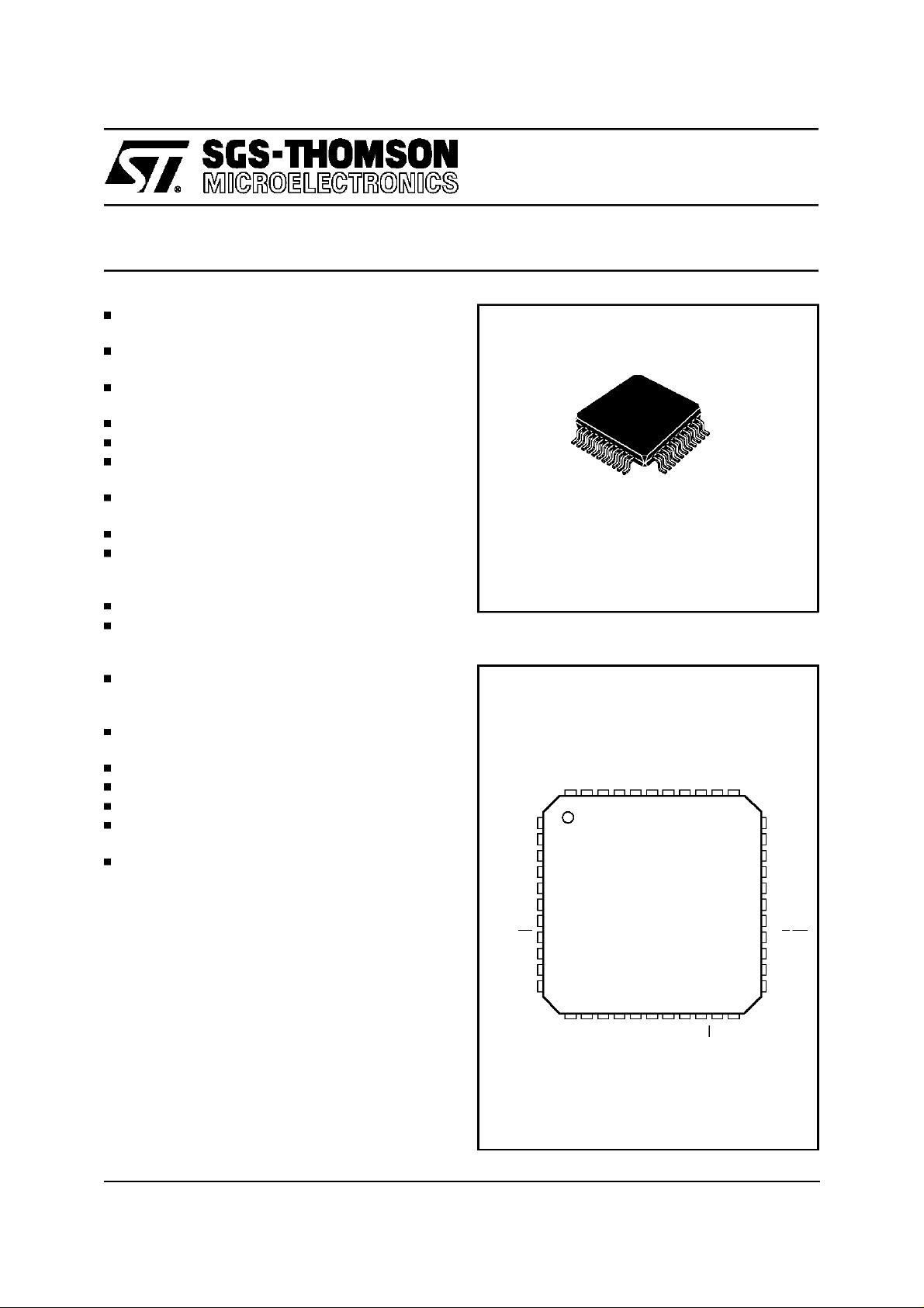
STLC5432
TQFP44 (10 x 10)
ORDERING NUMBER: STLC5432Q
PIN CONNECTION (Topview)
P0
LI1
VT
P1
GNDA
GNDD
SA/RESET
DIN
A/D0
A/D1
A/D2
A/D3
INT
RCLI
BRDI
DOUT
LI2
1
2
3
4
5
6
7
8
9
10
11
RCLO
BRDO
AS/ALE
XTAL1
3940414344 42
1716151312 14 22212018 19
XTAL2
VCCD2
DPI
VCCD1
PRELIMINARY DATA
VCCA
CS
LO1
LO2
34353638 37
33
BXDI
32
AL0
31
AL1
30
A/D7
29
A/D6
28
A/D5
27
A/D4
26
R/W/WR
25
LFSX
24
LFSR
23
LCLK
HCR
LCR
DS/RD
D93TL043D
BXDO
July 1996
1/46

STLC5432
PIN DESCRIPTION
Name Pin Type Function
Positive power supply inputs for the digital (V
VCCD1
VCCD2
VCCA
GNDD
GNDA
LI1
LI2
18
17
34
1
44
40
42
VT 41 O Positive power supply output for fixing reference voltage to the receive transformer.
L01
L02
36
37
XTAL1 15 I The master clock input which requires either a parallel resonance crystal to be tied
XTAL2 16 O The output of the crystal oscillator, which should be connected to one end of the
HCR 19 O High clock received, bit clock. When the device has recovered the clock from the
LCR 20 O Low clock received, frame clock. When the device has recovered the clock from the
BRDO
RCLO
BRDI
RCLI
12
14
10
9
BXDO 22 O Binary TransmitData Output, 2048kbit/s oroutput clock at 64kHz.
BXDI 33 I This binary signal can replace BXD internal signal to be encoded if SELEX bit (CR1
DOUT 11 O Data Output. 30 B+D primary access data received from the line.Data can be shifted
DIN 3 I Data Input : 30B+D primary access data to transmit tothe line.Data can be shifted in
I
I
microprocessor interface signals (V
I
connected together.
). They must be +5 Volts and must be directly
CCD2
) and analog (V
CCD1
) sections and for
CCA
IINegative power supply pins which must be connected together close to the device. All
digital and analog signals are referred to thesepins, which are normally at the system
ground.
I
Receive HDB3 signal differential inputs from the line transformer.
I
Typical value is 2.375V
OOTransmit HDB3 signal differential outputs to the line transformer.When used with an
appropriate transformer, the linesignal conforms to the outputspecifications in CCITT
with a nominal pulse amplitude of 3 volts for a 120Ω load on line side.
between this pin and XTAL2, or a clock input from a stable source. This clock does
not need to be synchronized to the system clock.
Crystal specifications = 32764 kHz ± 50 ppm parallel resonant; RS ≤ 20Ω loaded with
33pF to GND each side.
crystal if used.
HDB3 signal, HCR signal is synchronized to the remote circuit. The HCR frequency is
either 8192kHz if 8MCR bit of CR1 Register is put to 1 or 4096 kHz if 8MCR is set to
0.
HDB3 signal, LCR signal is synchronized to the remote entity.
The LCR frequency is 8 kHz if 8KCR bit is set to 1, or 4 kHz if 8KCR bit is set to 0.
When the remote clock is not recovered, HCR and LCR frequency are synchronized
to master clock (16384 kHz).
HCR and LCR can be used by the system inTerminal Mode.These two clocks can be
used by the transmit function of the device.
OOBinary Receive Data Output, 2048 kbit/s or 64kbit/s.
Receive Clock output, 2048 kHz or 64kHz.
After decoding, Binary Data and clock associated are provided for different
applications.
IIBinary Receive Data Input. 2048 kbit/s.
Receive Clock Input 2048 kHz.
Before encoding Binary Data is provided to different applications (Optical Interface for
instance). Local clock is associated to thisdata.
Register) is set to 1.
out from the tristate outputDOUT at the LCLK frequency on the rising edges during
all the time slots,except Time Slot Zero inaccordance withTSOE bit (CR1Register).
NB : If parallel micro-interface is selected, DOUT is at high impedance after Reset.
DOUT is at low impedance after writing CR4 register.
at the LCLK frequency on the falling edges during all the time slots,except Time Slot
Zero, in accordance with TSOE bit (CR1 Register).
2/46

STLC5432
PIN DESCRIPTION(continued)
Name Pin Type Function
LCLK 23 I Local Clock : this clock input determines the data shift rate on the two digital
LFSR 24 I Local Frame Synchronization for the Receiver. This clock input defines the start of the
LFSX 25 I Local Frame Synchronizationfor the Transmitter. This clock input defines the start of
AL0,
AL1
32
31
multiplexes. Thisclock frequencycan be indifferently2048, 4096, 8192or 16384kHz.
Data Out and Data In rate is always 2048 kbit/s when Serial Interface microprocessor:
an internal automatic mechanism divides by two the frequency if 4096 kHz.
frame on the digital multiplex Data (pin DOUT). This clock frequency can be
indifferently 8 kHz or a submultiple of 8 kHz.
the frame on the digital multiplex Data (pin DIN). This clock frequency can be
indifferently 8 kHz or a submultiple of 8 kHz.
If submultiple of 8 kHz, LFSX defines the start of even frame on DIN.The TSO of this
even frame will contain the Frame Alignment Signal(FAS) on the line.
OOAlarm 0 Output, alarm 1 Output. These pins are opendrain outputs which are
normally in high impedance state.
AL1 AL0 Alarm definitions
Z Z Frame or Multiframerecovered,
0Volt Z Frame or Multiframe recovered,
Z 0Volt Frame and Multiframe lost, AIS
0Volt 0Volt Frame and Multiframe lost, AIS
DPI 38 I DPI input: The internal DPLL is synchronizedeither by the signalapplied on DPI input
SA/RESET 2 I Stand Alone : When this pin is connected to 5 Volts, the device works without
P0, P1 39, 43 I Processorinterface. These two input pins define the microprocessor interface
AS/ALE 13 I Address Strobe/Address Latch Enable. Input
CS 35 I Chip Select.A high level on this input selects the PRCD for a read write operation.
R/W/WR 26 I Read/Write/Write Data. Input.
DS/RD 21 I Data Strobe/Read Data. Input.
A/D0toA/D7 4 to 7;
27 to 30
INT 8 O Interrupt Request. Thesignal is activated low when the PRCD requestsan interrupt. It
(if DPIS bit of CR5 register is =0) orby the 2MHz clock recovered from the line.
microprocessor. The configuration is given by the values per default of programmable
registers. BRDI and BXDI must not be used.
RESET: When this pin is put to 5 Volts during 100 ns at least every programmable
register is reset (value per default). When this pin is set at zero Volt, the type of
microprocessor is selected by P0, P1 pins.
chosen.
I/O
Address/Data 0 to 7. Input-Output.
is an open drain output.
P1 P0 Microprocessor Interface
----------------------------------------------------------------------------------0 0 Serial MicroprocessorInterface
0 1 ST9 MicroprocessorInterface
1 0 Multiplexed Motorola processor interface
1 1 Multiplexed Intel processorinterface
A bit received is 0.
A bit received is 1
Alarm Indication Signal is detected.
Alarm Indication Signal is not detected.
3/46
STLC5432
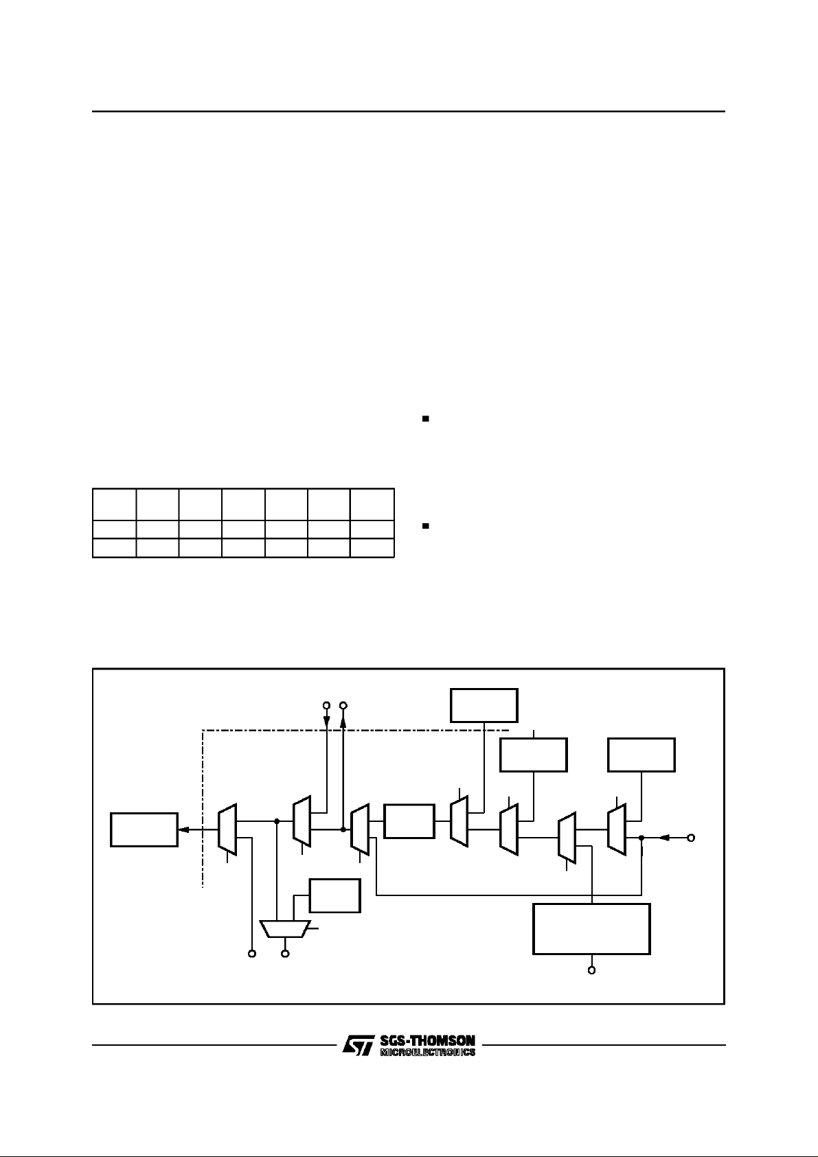
BLOCK DIAGRAM
BRDO BRDI
µP
ELASTIC
MEMORY
BRD
LCLK
PROGRAMMABLE
INTERFACE
REGISTERS
4
LOOPBACK
2
LOOPBACK
3
LOOPBACK
BXD
LFSR
DOUT
64 BYTES
SYNCHRONIZATION
AB
DIN
LFSX
D
MULTIFRAME
GENERATION
64KHz
CLOCK
D93TL044F
BXDI BXDO
4/46
RCLO
Q=32764KHz
LCRHCR
DPLL
HDB3/BIN
DECODER
RD-
RD+
DATA
CLOCK
RECOVERY
A
From A, B or DIN
PSEUDO
RANDOM
SEQUENCE
PSEUDO
RANDOM
SEQUENCE
1
LOOPBACK
2Mb/s
S2/T2
INTERFACE
To D or DOUT
GENERATOR
ANALYZER
BIN/HDB3
ENCODER
ALARM
SIGNALS
LINE
DRIVER

STLC5432
ABSOLUTE MAXIMUM RATINGS
Symbol Parameter Value Unit
V
to GND Supply Voltage to Ground 7 V
CC
V
I
I
LO1,IOL2
I
C
T
stg
T
L
THERMAL DATA
Symbol Parameter Value Unit
R
thj-amb
Voltage at any digital or analog input VCC+1 to GND-1 V
Current at LO1 and LO2
100 mA
±
Current at any digital or analog input ±30 mA
Storage temperature range -65 to +150 °C
Lead Temperature (soldering, 10s) +300 °C
Thermal Resistance Junction to ambient Max. 50 °C/W
ELECTRICALCHARACTERISTICS (VCC=5V±5%, T
fied at V
CC
= 5V,T
=25°C; all signalare referencedto GND,unlessotherwise specified.)
amb
= 0 to 70°C; Typical characteristicsare speci-
amb
Symbol Parameter Test Condition Min. Typ. Max. Unit
DIGITAL INTERFACE
Vil Input Low Voltage All digital inputs 0.8 V
Vih Input High Voltage All digital inputs 2.2 V
Vilx Input Low Voltage XTAL1 input 0.5 V
Vihx Input High Voltage XTAL1 input V
Vol Output Low Voltage I
= 7mA for pins AL0, AL1,
L
-0.5 V
CC
0.4
INT, DOUT, HCR, LCR.
0.4
Voh Output High Voltage I
All other digital outputs:
I
= 1mA
L
= 7mA for pins AL0, AL1,
L
2.4
INT, DOUT, HCR, LCR.
All other digital outputs:
I
= 1mA
L
2.4
Iil Input Low Current Any digital input, Gnd < Vin < Vil 10
Iih Input High Current Any digital input, Gnd < Vin <
V
CC
Ioz Output Currentin High
Impedance (tri-state)
All digital tri-state I/Os without
internal pull-up or pull-down
10 µA
10
resistor.
LINE INTERFACE FEATURES
Zin Differential Input Resistance DC measurement between LI1
200 K
and LI2 with the equalizer not
connected
Vin Rx sensitivity Relative to LI1/LI2 pins with
0.6 Vpk
fixed detection threshold
Vpk75 Transmit amplitude 75Ω at transformer secondary 2.14 2.37 2.60 Vpk
Vpk120 Transmit Amplitude 120Ω at transformer secondary 2.7 3 3.30 Vpk
Sym Pulses Symetry 75Ω or 120Ω at transformer
5%
secondary
Zero Zero level % nominal amplitude 10 %
Pwdth Tx pulses width at 50% of peak amplitude 219 244 269 ns
Zout Differential Output Resistance 1 Ω
MASTERCLOCK
MCLK MCLK Frequency 32.764 MHz
MCLK Frequency tolerance –50 50 ppm
JITTER PERFORMANCES(for jitter transfer function and admissible jitter please report to the corresponding
characteristics plotted in following page).
Intrinsic jitter Filter 20Hz - 100KHz 0.125 UI
Intrinsic jitter Filter 700Hz - 100KHz 0.12 UI
V
V
V
V
A
µ
A
µ
Ω
5/46
STLC5432
ELECTRICALCHARACTERISTICS (continued)
Symbol Parameter Test Condition Min. Typ. Max. Unit
POWER CONSUMPTION
Icc75 Active Current(including line
current)
Icc120 Active Current(including line
current)
TRANSFORMER SPECIFICATION FOR75Ω
L:M:N: Turns ratioes 1.57:1:1
RL L Windings Resistance 0.23
RMN M and N winding resistances 0.11 Ω
LL Inductance of winding L F = 100KHz, Vrms = 100mV 2 mH
Ls Leakage inductange of a
winding, the other being short
circuited
Ck Inter winding capacitance F = 100KHz, Vrms = 100mV 15 pF
TRANSFORMER SPECIFICATION FOR120Ω
L:M:N: Turns ratioes 2:1:1
RL L Windings Resistance 0.2
RMN M and N winding resistances 0.1
LL Inductance of winding L F = 100KHz, Vrms = 100mV 2 mH
Ls Leakageinductange ofawinding,
theother beingshortcircuited
Ck Inter winding capacitance F = 100KHz, Vrms = 100mV 15 pF
XTALL SPECIFICATIONS
Co Motional capacitance 0.2 pF
Cc Shunt capacitance 6 pF
Lo Inductance 4.718 mH
Rs Serial resistance 15
CL Load (corresponding to two
33pF capacitors connected to
XTAL1 and XTAL2 pins on the
application schematic)
DYNAMIC CHARACTERISTICS
tpd LCLK high to DOUT valid
LCLK high to BXDO valid
XTAL1 high to HCR high or low
tpdz LCLK high to DOUT HZ 150pF; 7mA 50 ns
td HCR high to LCR high or low
RCLOhighto BDROhighorlow
ts All data inputs to clock low 10 ns
th Clock low to alldata inputs 10 ns
random output (50% of ones) 40 mA
random output (50% of ones) 40 mA
F = 100KHz, Vrms = 100V 0.3 µH
F = 100KHz, Vrms = 100mV 0.2 µH
20 pF
150pF; 7mA
50pF; 1mA
150pF; 7mA
150pF; 7mA
50pF; 1mA
–20 20 ns
50 ns
Ω
Ω
Ω
Ω
6/46
Figure 1: ReceiverDiagram
STLC5432
RCLODPILCRHCR
BRDO BRDI
1
DATA
64Kb/s
LP3
SIG
A
1
1
HDB3/BIN
DECODER
64 x 8
SELER
DOUT
1
B
MEMORY
RDS
-1
n
2
GENERATOR
A
B
-1
n
SAV
2
SGV
RXRD
ANALYZER
BIN/HDB3
DIAGRAM
TRANSMITTER
ENCODER
DIN
PULSE
SINGLE
D93TL046C
DATA
CLOCK
RECOVERY
1
DPLL
DPIS
1
ASP
1
LP1
A
S2/T2
2Mb/s
INTERFACE
ALARM
1
AIS
A
7/46
STLC5432
INTRODUCTION
This single chip CMOS Device interfaces the
physical multiplex of the application to the physical CEPT transmissionlink at 2048kb/s.
STLC5432 contains analog and digital functions
to implement line interface function and frame
synchronization. It meets pulse shape and jitter
specifications in accordance with CCITT Recommendations and CEPTstandards.
FUNCTIONAL DESCRIPTION
1. LINEINTERFACE
1.1 Receiver
The receive input signal should be derived via a
transformer of the same type used for the transmit direction. The suggested transformer is the
VAC L4097-X004 or equivalent for the 75 ohms
case and the VAC 4097-X012 or equivalent for
the 120 ohms case. The electrical models of the
transformers are summarized in the following table :
Loads
(Ω)
75 1.57 :1:1 ≤0.3 ≤15 ≥2 0.11 0.23
120 2:1:1 ≤0.2 ≤15 ≥2 0.10 0.20
Ls
n
(µH)Ck(pF)Lh(mH)
Rcul
(Ω)
Rculll
(Ω)
with:
n: Windingratioes
Ls: Leakageinductance
Figure 2: TransmitterDiagram
Ck: Interwinding capacitance
Lh: Principalinductanceof
windings
RcuI and RcuIII : DC resistancesof
windingI and III.
Wiring between the transformer and the circuit
should respect the application schematic given in
annex.(see fig4).
The internalfixed thresholdis set to 200 mV over
the common mode voltage VCM (VCM = 2.375 V
nominal) to insure the specified transmission
range with a good noise immunity.
Two options are provided for special applications
requiringimproved transmissionranges:
AUTO-ADAPTATIVETHRESHOLD:
Using the configuration register CR4 (AVT), a
peak amplitude detectorcircuit is connected to
the received signaland after digital processing,
an adaptative threshold value equal to 3/8 of
the peak value is obtainedat the output of a D
to A converterand used for data detection.
AUTOMATIC EQUALIZER: connecting two externalcapacitorsof100pFin seriesbetweenthe
transformerandthe circuitsinputs,and usingthe
configuration register CR4 (EQV), the circuit will
selectautomatically a pre-compensationfilter for
long line configuration (see application schematicon figure3 and4 givenin annex).
8/46
BIN/HDB3
ENCODER
1
SELEX
BXDI BXDO
RD RX
1
LP2
64KHz
CLOCK
1 SIG
TM
DOUT
SGV
n
-1
2
GENERATOR
LP4
CRC4
1
1
RDS
1
D
1
SIG
ADAPTOR: WHEN
DATA IN CLOCK IS
64KHz, DATA
CLOCK AT 2048KHz
BXDI
TS
GENERATOR
TSO
1
AT
OUT
DIN
D93TL045B

STLC5432
Using bothoptions allow the reception of a signal
attenuatedup to 12dBat 1024kHz.
The Clock recovery is performed by a first PLL
that guaranties the CCITT I431 requirements for
the allowedJitter, see Figure 23, this clock, RCL,
is usedinternallyandas local clock.
A second DPLL starting from this RCL clock attenuate the Jitter,to fulfil the CCITT I431, see figure 8, this DPLL generate HCR, bit clock, and
LCR frame clock, practically without Jitter.
1.2 Transmitter
The line driver outputs are designed to drive the
suitable transformer mentioned in the previous
section. The transformerresults in a signal amplitude of 3 voltson the linewhich meet G.703 pulse
shape for a 120 ohm load (2.37 volt for a 75
ohms load).
A special test mode is provided to check the
pulse template according to the CCITT mask by
using the configurationregister CR3 (ASP).
When the ALS command is valid, consecutive
logical ”ones” are transmittedon theline.
When APS command is valid, consecutive 1, 0,
1... 1, 0,1, 0... are transmitted on the line.
2 CODING
2.1 HDB3/BINDECODING
The two constituents of the data signal are de-
coded and the binary Receive Data Signal (BRD)
is processedbythe next functions.
2.2 BIN/HDB3ENCODING
The binary transmit data signal (BXD) is encoded.
The entire data stream, including all the time
slots, is scanned for an occurence of four consecutive zeros.
Such occurence is replaced by the appropriate
HDB3 code.
3. BINARYINPUT-OUTPUT
STLC5432 can directly interface binary data
stream by means of the 6 dedicatedpins:
BRDO, RCLO,BRDI, RCLI,BXDOand BXDI.
This allows the use of STLC5432also for particular cases as for optical fiber or for different purposes. The functions of these 6 pins are defined
by the SIGbit (SIGR register).
3.1 SIG = 0
When the bit SIG = 0 the binary data are ex-
changed at 2048KHzand the 6 extrapins are defined hereafter.
3.1.1 Extrapinsfor receive data
The BRDOand RCLO output pins deliver respec-
tively BRD binary receive data at 2048kb/s and
the remoteclock recovered at 2048kHz.
Two BRDI and RCLI input pinscan receive external binary receive data at 2048kb/s and the receiveclockassociated at 2048kHz.
The SELERcommand replaces BRD internal signal with BRDI signal.
3.1.2 Extrapins for transmitdata
The transmit binary data output pin BXDO deliv-
ers transmitbinary data BXD.
Input pin BXDI can receive external binary trans-
mit data.
The SELEXcommand replaces BXD internal sig-
nal with BXDIsignal.
3.2 SIG = 1
When SIG = 1, a signaling channel at 64 kb/s is
implemented.
3.2.1 Extrapins for Receivedata
BRDO and RCLO output pins deliver respectively
receive data at 64kb/s selected by an internal
Time Slot Assigner and the receive clock associated at 64kHz. In this case, BRDI and RCLI are
not used.
3.2.2 Extrapins for TransmitData
Output BXDO delivers the 64kHz clock for an ex-
ternal application. This external entity delivers
data at 64kb/son the rise edge of the clock.
Input BXDIshifts data at 64 kb/s on the fall edge
of the 64kHzclock.
The same Time Slot Assigner is used by transmitter and receiver(See SIGR Register).
4 LOOPBACK
4.1 LOOPBACK1
When LP1 Command is valid (LP1 bit high, see
CRC3 register), output data signal replaces input
data signal. Then, the recoveryclock functionprovides the local clock. The loopbackis transparent
if AIS is at 0. If AISX is at 1, consecutive logical
”ones”are transmittedon theline.
4.2 LOOPBACK2
LP2 Command (LP2 bit high, CR3 register) re-
places BXD and XCLK signals (respectively Binary Transmit Data and transmit clock) with BRD
and RCLK (respectively Binary Receive data and
its clock recovered).
4.3 LOOPBACK3
LP3 Command (LP3 bit high, CR3 register) re-
places BRD and RCLK (respectively Binary Receive Data and its clock recovered) with BXD and
9/46
STLC5432
XCLK (respectively Transmit Data and its clock
associated). Frame and multiframe generated by
the transmitter of the circuitare processed by the
receiver of the circuit, without encoding and decoding.
4.4 LOOPBACK4
LP4 Command replaces Data in with Data out
near of DIN and DOUT pins (See LP4R register).
5 FRAME ALIGNMENT
Time slot 0 is used for the synchronization
(G.706). At softwareReset Frame and Multiframe
are lost and a new research of FASand MFAS is
launched.
5.1 LOSS OF FRAMEALIGNMENT
Frame alignment will be assumed to have been
lost :
– eitherwhen three consecutiveincorrect frame
alignmentsignals have been received,
– or when bit 2 in time slot 0 in odd frames has
been received with an error, i.e. at0, on three
consecutiveoccasions,
– or when 915 errored CRC blocks out of 1000
have been detected.
5.2 FRAME ALIGNMENT RECOVERY
Frame alignment will be assumed recovered
when the followingsequence is detected:
– Detection of the correct Frame AlignmentSig-
nal, FAS
– detectionof bit 2 of 32nd byte after FAS,at 1.
– detectionof the correct Frame Alignment sig-
nal in the 64th byte after the first FAS de-
tected.
5.3 MULTIFRAME ALIGNMENTRECOVERY
Multiframe Alignment will be assumed recovered
when at least two valid multiframe alignment signals MFAShave been detectedwithin 8 ms.
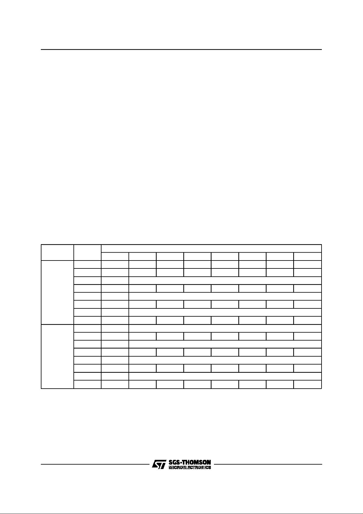
Table 1: CRC4 Multiframe StructureG.704
Sub
Multiframe
I
II
FAS: Frame AlignmentSignal in each even Time Slot.
MFAS: Multi Frame Alignment Signal 0 0 1 0 1 1
E1–E2: CRC4 error Indication bits
C1 to C4: Cyclic Redundancy Check 4 (CRC4) bits
A: Remote Alarm Indication
Sa4 to Sa8: Five bits in each odd Time Slot
Sa61 to Sa64: ETSI bits
Frame
0C10011011
1 0 1 A Sa4 Sa5 Sa61 Sa7 Sa8
2C2 F A S
3 0 1 A Sa4 Sa5 Sa62 Sa7 Sa8
4C3 F A S
5 1 1 A Sa4 Sa5 Sa63 Sa7 Sa8
6C4 F A S
7 0 1 A Sa4 Sa5 Sa64 Sa7 Sa8
8C1 F A S
9 1 1 A Sa4 Sa5 Sa61 Sa7 Sa8
10 C2 F A S
11 1 1 A Sa4 Sa5 Sa62 Sa7 Sa8
12 C3 F A S
13 E1 1 A Sa4 Sa5 Sa63 Sa7 Sa8
14 C4 F A S
15 E2 1 A Sa4 Sa5 Sa64 Sa7 Sa8
12345678
TIME SLOT ZERO BIT NUMBERS
10/46

STLC5432
5.3.1 Typical case
Remote entity transmits Frame Alignment Signal
(FAS) and MultiframeAlignment Signal(MFAS).
As soon as lost of Frame Alignment is occured
(LOF = 1), the local receiver recovers FAS from
254 up to 500µs after. As soon as FAS is recov-
ered (LOF= 0), thelocal receiver recoversMFAS
from 4 up to6ms after.
5.3.2 Old ExistingEquipmentCase
Remote entity transm its Frame Alignment Signal
(FAS)withoutMultiframe AlignmentSignal(MFAS ) .
As soon as lost of Frame Alignment is occured
(LOF=1), the local receiver recovers FAS from 254
up to 500µs after. Then LOF = 0, and 400msafter
thelocalreceiverindicatesthattheMultiframeAlignementSignalhasnotbeenrecovered(MFNR =1).
5.3.3 ParticularCase:SpuriousFrameAlignment
Signal
Local receiver receives true FAS and true MFAS
among several spuriousFAS.
Multiframe Alignment signal (MFR=1) is recovered
from 8 to 400ms after the Frame Alignmentsignal
is recovered (LOF=0). Then, this FAS is either a
spurious one (the ”Spurious Timeslot Zero” is carryingFASwithoutMFAS), ortrue FAS.
Anyway, when the Multiframe Alignmenthas been
recovered (MFR=1), the good Frame Alignment
Signal is taken into account and data are loaded
intothe Frame Memoryat thegood location.
SeeFig. 13synchronizationalgorithm.
5.3.4 WorstCase
Local receiver receives true FAS and true MFAS
among several spurious FAS and several spurious MFAS.
In this case, if the circuit has recovered a spurious FAS and MFAS, the CRC blocks will be detected with an high error rate. As soon as 915 errored CRC block within 1000 will be detcted, the
MFAS will be assumedas spuriousanda new research starts at the point just after the location of
the assumed spuriousFrame Alignement Signal.
5.4 TransmitterSIDE
The Frame Alignement Signal is transmitted continuously on the transmitterside, with bit 1 of TS0
at logical1.The MFASsignal is transmittedin accordance with NMF bit register (CR5 Register):if
NMF is programmed to ”1” Logic, no MFAS is
transmitted; if NMF is programmed to ”0” Logic
the MFAS signal is transmittedcontinuously.
Table 2.
LOF MFR MFNR RECEIVER STATE
1 0 0 FAS or MFAShas been lost.
State: Research of FAS
0 0 0 FAS has beenrecovered.
State: Research of MFAS
0 1 0 FrameandMultiframerecovered
State: Good working.
0 0 1 Frame recovered.
State: Good working without
multiframe received from
transmitting side.
6 Interfacingwith themicroprocessor
The device can work in one of the 3 following
modes:
– Parallel microprocessor InterfaceMode
– Serial microprocessorInterfaceMode
– Withoutmicroprocessor : StandAlone Mode.
The choiceis done by means of the SA/Reset,P0
and P1 pins.
6.1 ParallelMicroprocessorInterfaceMode
The microprocessor can read (or write) the regis-
ters of the STLC5432 using the fifteen parallel Interfacepins.
The use of TSO (Time Slot Zero) of DIN and
DOUT digital multiplex is defined by TSOE bit of
CR5 Register.
– If TSOE = 1, TSO on DIN multiplex Input is
used to transfer Sa4 to Sa8 bits to the line
and TSO on DOUT multiplexoutput isused to
transferSa4to Sa8bits fromthe line.
– If TSOE = 0, DOUT output is high impedance
during TSO, and DIN Input ignores data during TSO.
6.2 SerialMicroprocessor InterfaceMode
Fifteen parallel Interface pins are ignored, they
are tied to ground. In this mode, the time slots 0
of internal multiplexesare considered like a channel used by the devices and the control entity located in the system to communicate. This channel can be switched across a switching network
-or not- beforeits final destination.
The message is constituted by two bytes which
are transmitted on two consecutive Time Slots
Zero.
The bits of word are numbered 0 to 7, bit 0 is
transmittedfirst. Whenthe bit 7 ofa byte is 0,this
byte is the first word of the message.
The bit 6, of the first word, is R/W bit:
R/W = 1. Message to read a register whose address is designated by the following bits of the
word ( A 0/5).
11/46

STLC5432
R/W = 0. Message to write a register, addressed
by the bitsA0/5.
The bit 7 of following byte is 1 and the seven
D 0/6 bits are datato load into register.
To transfer one message,250µs are necessary.
Between two messages, the bits are 1 during
TS0. See fig.7 for details.
6.2.1 Reading of a register
The remote entity connected to the DIN and
DOUT multiplexes can request reading of a register if it transmits, during TSO, on DINthe address
bit A0/5,the R/Wbit at 1 and the last bit at0. The
following word, ending with 1, isnot takeninto account by the device. The device returns two
words during TSOof DOUT:
–The first word begins with 0, R/W bit is put to
1, the address bits of the register are transmitted.
–The second word begins with 1, then seven
databits of the registerare transmitted.
6.2.2 Writing of a register
The remote entity connected to the DIN and
DOUT multiplexes can request writing, then it
transmits the first bit at 0, thesecond bit at 0 and
the register address A 0/5 during TSO of DIN.
The following word begins with 1 and seven next
bits are Data to load into register. There is no acknowledge after writing. The writing messages
can be transmittedconsecutively.
6.3 Stand Alone Mode
Whatever the received frequency on LCLK pin
(2.048kHz or 4.096kHz), the device automatically
fits and always works at 2.048kHz.When SA pin
is at 1, the multiframe research is automatically
launched after each lost of frame and the device
provides the following alarmson DOUTduring the
Time Slot 0:
7
F/S SKIP AR MFNR LOF B AIS LOS
LOS Lossof signal
AIS Alarm IndicationSignal
B If LOF = 1, thenB = 915
If LOF = 0, thenB = WER
LOF Loss of Frame
MFNR MultiFrame Not Recovered
AR ABit Received
SKIP Jump
F/S Fast/Slow.
Bits definitions are the same than bits definitions of
ALR, CAR1 and CAR2 Registers. These bitsrepresent the curre nt stateof the line; DI Nis ignoredduringTime SlotZero.
7 RESET
During HardwareReset (Pin : SA/RESET):
– Alltheprogrammableregistersareconfigurated
withthe defaultvalue.
– Interrupts are not generated (INT PIN is high
impedance).
– The researchof Multiframeis alwaysactive.
AtSoftwareReset(addressing theResetregister):
– The registers are configuratedwith the default
value only.
AfterReset:
– The registers may be configurated with any
value.
8 INTERRUPT
All the bits of Alarm Registers generate an interrupt if they are not masked, exceptSLC (CAR2).
An alarm generates an interrupt if the mask bit
associated is 0. If a temporary event is detected
from the line. ALR Alarm Register, CAR1 and
CAR2 Complementary Alarm Registers can be
read after interruptor bypolling.
In this last case, these Alarm Registers can be
consideredlike particular statusregisters.
If a temporary event is detected from the line,
then the appropriate bit is put to one. After reading by the microprocessor, this bit is put to zero
until new event.
If a permanent state occurs, then the appropriate
bit is put to one. Afterreading by the microprocessor, this bit remains at one until disappearance of
the cause.
8.1 ParallelInterfaceMode
ALR Alarm Register, CAR1 and CAR2 Comple-
mentary Alarm Registers can be read after interrupt or by polling.
In this last case, these Alarm Registers can be
consideredlike particular statusregisters.
INT pin is put to 0 volt. The microprocessorreads
AlarmRegister.
For example, after reading the ALR and CAR1
registersthemicroprocessorcould act as follows:
– If SCbit (clock1 second)is 1, then the micro-
processorreads fault counter registers.
– If EXT1 bit (EXTENSION1) is 1, then the mi-
croprocessor reads Complementary Alarm
Register1.
– If TSOR (or Sa6R) bit of CAR1 is 1, the mi-
croprocessorreads TSORR (or Sa6RR) Register
12/46

STLC5432
8.2 Serial InterfaceMode
When an Alarm bit isput to 1 in ALR (Alarm Reg-
ister), this bit generates automatically the transmission of two bytesmessage onto DOUTduring
Time slot 0 with :
– The first bit of the first byte at 0; the second
bit is at 0 and after the address bits of Alarm
Register.
– Thedataof the ALR(Alarm Register) is the sec-
ondbyte.
NB : When TSOR or Sa6R bit of the CAR1
(ComplementaryAlarm Register 1) is put to ”1”, it
generates a message in which there are address
and data of TSORR Register (if TSOR bit is not
masked), or address and data of Sa6RR register
(if Sa6R is not masked).
If the fouroccurencesto transmit a message are simultaneous,thepriorityorderis:
Priority1 : Transmissionof Alarm
Registerdataif an alarm
has beendetected.
Priority2 : Transmissionof Register
data afterreadingmessage
fromremoteentity.
Priority3 : Transmissionof TSORR
data afterloadingof this
register.
Priority4 : Transmissionof Sa6RR
data afterloadingof this
register.
8.3 Stand AloneMode
Interruptsare notgenerated.
AL0, AL1 pins indicate the current state of three
alarms : LOF, AIS, A bit received and DOUT pin
indicates the current state of nine alarms during
time-slotzero (SeePar. 6.3).
13/46

STLC5432
Table 3: The registersand theirbits.
After
ADD
(Dec.)
Reset
(Hexa)
0 NOT USED
1 RESET 1 DUMMY REGISTER W 15
2 88 ALR 1 EXT1 AR SC LOF 915 AIS LOS R 15
3 FF AMR 1 MEXT1 MAR MSC MLOF M915 MAIS MLOS R - W 15
4 80 CAR1 1 EXT2 0 Sa6R TS0R ER CRCF WER R 15
5 FF CAMR1 1 MEXT2 Nu MSa6R MTS0R MER MCRCF MWER R- W 15
6 80 CAR2 1 PRSL PRSR MFNR MFR 0 SLC SKIP R 16
7 FF CAMR2 1 MPRSL MPRSR MMFNR MMFR Nu 1 MSKIP R - W 16
8 80 FCR1 1 F6 F5 F4 F3 F2 F1 F0 R 16
9 80 FCR2 1 F13 F12 F11 F10 F9 F8 F7 R 16
1080ECR11E6E5E4E3E2E1E0 R 16
11 80 ECR2 1 E13 E12 E11 E10 E9 E8 E7 R 16
1280PCR11P6P5P4P3P2P1P0 R 17
13 80 PCR2 1 P13 P12 P11 P10 P9 P8 P7 R 17
14 B8 ERTR 1 IT2 IT1 IT0 VT3 VT2 VT1 VT0 R - W 17
15 80 TS0RR 1 0 0 Sa4R Sa5R Sa6R Sa7R Sa8R R 17
16 9F Sa6RR 1 0 AR Sa5R Sa61R Sa62R Sa63R Sa64R R 17
17 X RES RESERVED: Avoid Addressing
18 9F TS0XR 1 WT AE Sa4X Sa5X Sa6X Sa7X Sa8X R - W 18
19 8F Sa6XR 1 WT Nu Nu Sa61X Sa62X Sa63X Sa64X R - W 18
20 X RES RESERVED: Avoid Addressing
21 90 SIGR 1 SHCR SIG STS4 STS3 STS2 STS1 STS0 R - W 18
22 80 LP4R 1 SLCR LP4 LTS4 LTS3 LTS2 LTS1 LTS0 R - W 18
23 84 CR1 1 MERA LTM 8KCR MCR1 MCR0 SELEX SELER R - W 20
24 80 CR2 1 DOHZ RDS1 RDS0 POL NR NX TM R - W 20
25 80 CR3 1 ASP Nu AISX ALS LP3 LP2 LP1 R - W 21
26 80 CR4 1 EQV AVT DEL DCP M2 M1 M0 R - W 21
27 80 CR5 1 TS0E APD NMF HCRD DPIS CENTER FROZ R - W 23
28 80 CR6 1 POLSa OSCD SaT Sa51 Sa50 Sa41 Sa40 R - W 23
29 80 CR7 1 AMI Sa81 Sa80 Sa71 Sa70 Sa61 Sa60 R - W 24
30 FF CR8 1 FILT SP Sa4P Sa5P Sa6P Sa7P Sa8P R -W 24
31 X RES RESERVED: Avoid Addressing
32 80 TCR1 1 SGV GTS5 GTS4 GTS3 GTS2 GTS1 GTS0 R - W 25
33 80 TCR2 1 SAV ATS5 ATS4 ATS3 ATS2 ATS1 ATS0 R - W 25
34 80 TCR3 1 CRCC EBC PELC PULS FASC ODTS TWI R - W 26
35 to 63 Reserved for the dietest: Avoid Addressing
Register
Name
bit 7 bit 6 bit 5 bit 4 bit 3 bit 2 bit 1 bit 0
Read/
Write
Page
Nu = Notused.
14/46
 Loading...