

GENERAL FEATURES
SINGLECHIP2B1QLINECODETRANSCEIVER
SUITABLEFOR ISDN, PAIR GAIN AND DECT
APPLICATIONS
MEETS OR EXCE ED S ETSI EUROPEAN
STANDARD
SINGLE5V SUPPLY
DIP28 AND PLCC44 PACKAGE
HCMOS3A SGS-THOMSON ADVANCED
1.2µm DOUBLE-METALCMOS PROCESS
ROUND TRIPDELAY MEASUREMENT
EXTENDED TEMPERATURE RANGE (-40°C
TO +70°C)
TRANSMISSIONFEATURES
160 KBIT/S FULL DUPLEX TRANSCEIVER
2B1Q LINE CODING WITH SCRAMBLER/DE-
SCRAMBLER
SUPPORTS BRIDGE TAPS, SPLICES AND
MIXED GAUGES
>70DBADAPTIVEECHO-CANCELLATION
ON CHIP HYBRID CIRCUIT
DECISIONFEEDBACKEQUALIZATION
ON CHIP ANALOG VCO SYSTEM
DIRECT CONNECTION TO SMALL LINE
TRANSFORMER
STLC5412
2B1Q U INTERFACEDEVICE
ENHANCED WITH DECT MODE
PRELIMINARY DATA
PLCC44
ORDERING NUMBER: STLC5412FN
Plastic DIP28
ORDERING NUMBER: STLC5412P
SYSTEM FEATURES
ACTIVATION/DEACTIVATIONCONTROLLER
ON CHIP CRC CALCULATION AND VERIFI-
CATION INCLUDING TWO PROGRAMMABLE BLOCKERROR COUNTERS
EOC CHANNEL AND OVERHEAD-BITS
TRANSMISSION WITH AUTOMATIC MESSAGE CHECKING
GCI AND µW/DSI MODULE INTERFACES
COMPATIBLE
DIGITAL LOOPBACKS
COMPLETE(2B+D)ANALOGLOOPBACKIN LT
ELASTIC DATA BUFFERS AND BACKPLANE
CLOCK DE-JITTERIZER
AUTOMODENT1 AND REPEATER
”U ACTIVATION ONLY”IN NT1
February 1999
This is preliminary information on a new product now in development or undergoingevaluation. Details are subject to change without notice.
IDENTIFICATIONCO DEAS PERGCISTANDARD
DECTFRAME SYNCHRONIZATION
EASILY INTERFACEABLE WITH ST5451
(HDLC & GCI CONTROLLER), STLC5464 /
STLC5465 AND ANY OTHER GCI, IDL or
TDM COMPATIBLEDEVICES
1/74

STLC5412
INDEX
DISTINCTIVE CHARACTERISTICS .......................................... Page 1
GENERAL DESCRIPTION....................................................... 5
PIN FUNCTION .................................................. .............. 6
FUNCTIONAL DESCRIPTION............................................. ....... 14
Digital Interfaces. . . . .....................................................
µW/DSI mode . . . . . . ....................................... ..............
µ
W Control Interface. . . . .................................... ..............
WriteCycle . . . . . . . . . . . . . . . . . . . . ........................ ..........
ReadCycle............................................. ............1414
Digital SystemInterface. . .................................................
GCI mode. . . . . . . .....................................................1518
Frame structure. . . . . . . . ...........................................
Physicallinks . . . . . . . . . ............................................
Monitor channel. . . . . . . . . . . . . . .....................................
C/I channel.. . . ...................................................
Line coding and frameformat . . . ...........................................
Transmitsection. . . . . . . . .................................................
Receivesection..........................................................
Elasticbuffers............................................................
Dectsynchronization.......................................................
Maintenancefunctions. . . . . ............................................... 26
M channel.. .....................................................
EOC.............................................................
M4channel.......................................................
SpareM5andM6bits...............................................
CRC calculation checking. . . . . . . . . . . . . . . . . . . ........................
Loopbacks. . . . . . . . . . . . . . . . . . . . . . . . . . . . . . . . . . . . . . . . . . . . . . . . . . . . ..
Identificationcode. . .....................................................
GeneralpurposeI/Os......................................................
Testfunctions.. . .........................................................
14
14
14
18
18
22
23
23
24
24
25
25
26
27
27
27
27
27
34
34
35
Turningonandoffthedevice................................................
Power on initialization . . . . . . . ......................................
Line signaldetection . ............................................
Power up control . . . . . ....................................... ....
Power down control. . . . . . . .......................................
Power up state . ........................................... ......
Power down state . . . . . . . . . . . . . . ...................................
Activationdeactivationsequencing.. . . . . . . . . . . . . . . . . . . . . . . . . . . . . . . ...........
Case of restricted activation. . . . . . . . . . . . ...................................
Resetof activation / deactivationstate machine. .................................
Hardwarereset...........................................................
Quietmode..............................................................
Automode...............................................................
35
35
35
35
36
36
36
36
36
36
36
36
37
Command/Indication(C/I) codes. . ..........................................
Internalregisterdescription. . . .. . . . .............. ..........................3741
Line interface circuit . . ...................................................
Boardlayout . . .........................................................5555
APPENDIX A: STATEMATRIX................................................... 60
APPENDIX B: ELECTRICAL PARAMETERS ........................................ 62
2/74
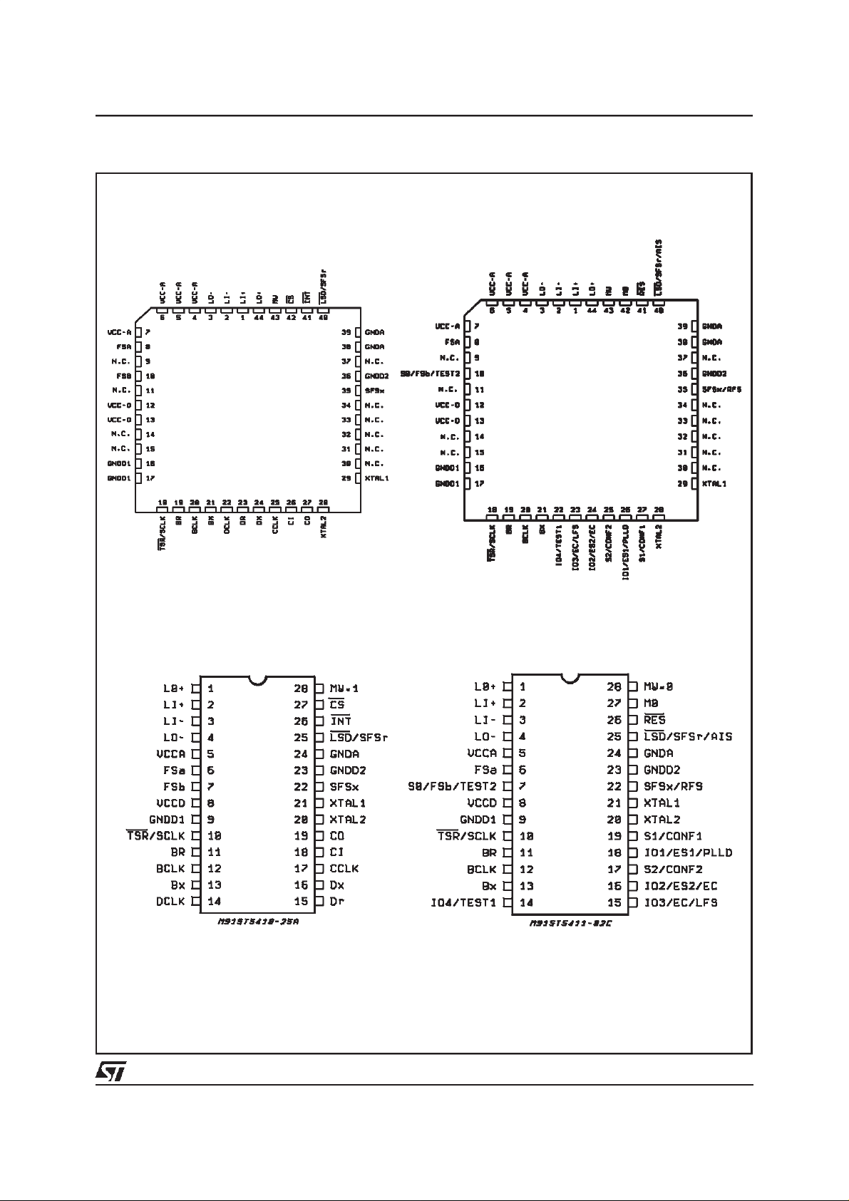
PIN CONNECTIONS (Topview)
STLC5412
PLCC44
MICROWIRE MODE
PLCC44
GCI MODE
DIP28
MICROWIRE MODE
DIP28
GCI MODE
3/74
STLC5412
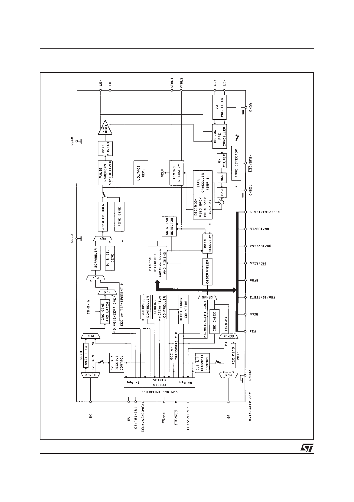
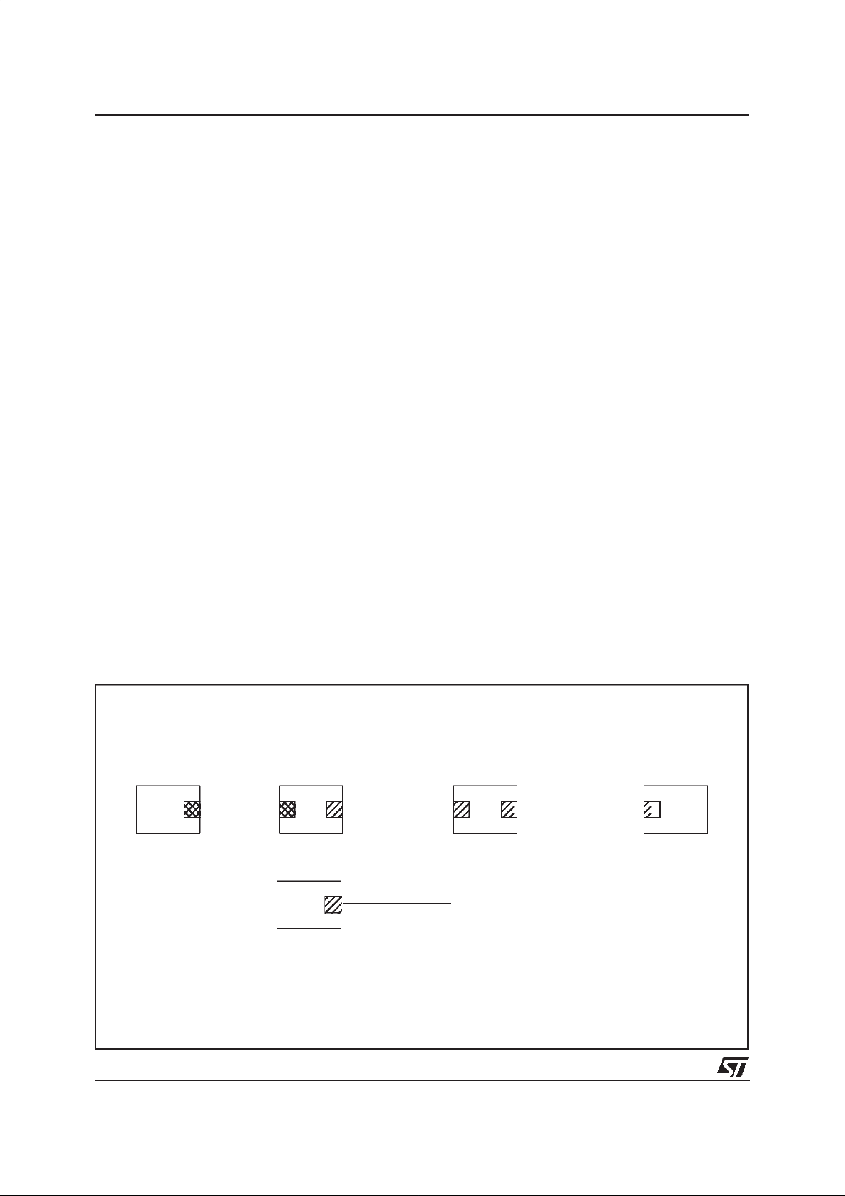
Figure 1: BlockDiagram.
4/74

STLC5412
GENERAL DESCRIPTION
STLC5412 is a complete monolithic transceiver
for ISDN Basic access data transmission on
twisted pair subscriber loops typical of public
switched telephone networks. The device is fully
compatible with ETSI ETRO80 and CSE (C32-11)
French specifications.
The equivalent of 160 kbit/s full-duplex transmission on a single twisted pair is provided, according to the formats defined in the a.m. spec.
Frames include two B channels, each of 64 kbit/s,
one D channel of 16 kbit/s plus an additional 4
kbit/s M channel for loop maintenance and other
user functions. 12 kbit/s bandwidth is reserved for
framing. 2B1Q Line coding is used, where pairs of
bits are coded into one of 4 quantumlevels. This
technique results in a low frequency spectrum
(160 kbit/s turn into 80 kbaud), thereby reducing
both line attenuation and crosstalk and achieving
long rangewith low Bit Error Rates.
STLC5412 is designed to operate with Bit Error
Rate near-end Crosstalk (NEXT) as specified in
european ETSI recommendation.
To meet these very demanding specifications, the
device includes two Digital Signal Processors,
one configured as an adaptive Echo-Canceller to
cancel the near end echoes resulting from the
transmit/receive hybrid interface, the other as an
adaptive line equalizer. A Digital Phase-Locked
Loop (DPLL) timing recovery circuit is also included that provides in NT modes a 15.36 MHz
synchronized clock to the system. Scrambling
and descrambling are performed as specified in
the specifications.
On the system side, STLC5412 can be linked to
two bus configurationsimply by pin MWbias.
MICROWIRE(µW/DSI) mode (MWpin = 5V): 144
kbit/s 2B+D basic access data is transferredon a
multiplex Digital System Interface with 4 different
interface formats (see fig. 2 and 3) providing
maximum flexibility with a limited pin count
(BCLK, Bx, Br, FSa, FSb). Three pre-defined
2B+D formats plus an internal time slot assigner
allows direct connection of the UID to the most
common multiplexed digital interfaces (TDM/IDL).
Bit and Frame Synchronisationsignals are inputs
or outputs depending on the configuration selected. Data buffers allow any phase between the
line and the digital interface. That permits building
of slave-slave configurations e.g. in NT12 trunkcards.
It is possible to separate the D from the B chan-
nels and to transfer it on a separate digital interface (Dx, Dr) using the same bit and frame clocks
as for the B channelsor in a continuousmode using an internallygenerated16 kHz bit clockoutput
(DCLK).
All the Control, Status and Interrupt registers are
handledvia a control channel on a separate serial
interface MICROWIRE compatible (CI, CO, CS,
CCLK, INT) supported by a number of microcontroller including the MCU families from SGSTHOMSON
GCI mode (MWpin = 0V). Control/maintenance
channels are multiplexed with 2B+D basic access
data in a GCI compatible interfaceformat(see fig.
4a) requiring only 4 pins (BCLK, Bx, Br, FSa). On
chip GCI channel assignement allows to multiplex
on the same bus up to 8 GCI channels,each supporting data and controls of one device. Bit and
Frame Synchronisation signals can be inputs or
ouputs depending on the configuration selected.
Data buffers, again, allow to have any phase between the line interfaceand the digital interface.
Through the M channel and its protocol allowing
to check both direction exchanges, internal registers can be configured, the EOC channel and the
Overhead-bits can be monitored. Associated to
the M channel, there are A and E channels for
enabling the exchanged messages and to check
the flow control. The C/I channelallows the primitive exchangesfollowingthe standardprotocol.
In both mode (µW and GCI) CRC is calculated
and checked in both directionsinternally.
In LT mode, the transmit superframe can be synchronized by an external signal (SFSx) or be self
running. In NT mode, the SFSx is always output
synchronizedby the transmit superframe.
Line side or Digital Interface side loopbacks can
be selected for each B1, B2 or D channel independently without restriction in transparent or in
non-transparent mode. A transparent complete
analog loopback allowing the test of the transmission path is also selectable.
Activation and deactivationprocedures, whichare
automatically processed by UID, require only the
exchange of simple commands as Activation Request, Deactivation Request, Activation Indication. Cold and Warm start up procedures are operated automatically without any special
instruction.
Four programmable I/Os are provided in GCI for
externaldevicecontrol.
5/74
STLC5412
PIN FUNCTIONS (no Specific Microwire / GCI Mode)
Note: allpin number are referredto Plastic DIP28 package.
Pin Name In/Out Description
1, 4 LO+, LO- Out, Out Transmit 2B1Q signal differential outputs tothe line transformer. When
2, 3 LI+, LI- In, In Receive 2B1Qsignal differential inputs fromthe line transformer.
5, 8 VCCA, VCCD In, In Positive power supply input for the analog and digital sections, which must
24, 923GNDA,GNDD1
GNDD2
10 TSR Out (LT configuration only)
SCLK Out (NT configuration only)
20 XTAL2 Out The output of the crystal oscillator, which should be connected to one end
21 XTAL1 In The master clock input, which requires either a parallelresonance crystalto
28 MW In MICROWIRE selection: When set high, MICROWIREcontrol interface is
In, In
In
used with an appropriate 1:1.5 step-uptransformer and the proper line
interface circuit the line signal conforms to the output specifications in ANSI
standard with a nominal pulse amplitude of 2.5 Volts.
be +5 Volts +/-5% and must be directly connected together.
Negative power supply pins, whichmust be connected together close to
the device.
All digital and analog signals are referred to these pins,which are normally
at the system Ground.
This pin is an open drain output normally in the high impedance state which
pulls low when B1 and B2 time-slots are active. It can be used to enable the
Tristate control of a backplane line-driver.
15.36 MHz clock output which is frequency locked to the receivedline
signal active as soon as UID is powered up except in NT1 Auto
configuration (active only if S line activation is requested)
of the crystal, if used. Otherwise, this pin must be left not connected.
be tied between this pin and XTAL2, or a logic level clockinput from a
stable source. This clock does not need to be synchronized to the digital
interface clocks (FSa, BCLK).Crystal specifications: 15.36 MHz +/-50ppm
parallel resonant; Rs≤20 ohms; load with 33pF to GND each side.
selected. When set low, GCI interface is selected.
PIN FUNCTIONS (specificMicro Wire mode)
Pin Name In/Out Description
6 FSa In Out Input or Output depending of the CMS bit in CR1 register, FSa is a 8 KHz
7 FSb In Out Input or Output depending of the CMS bit in CR1 register, FSb is a 8 KHz
11 Br Out 2B+D datas tristate output. Datasreceived from the line are shifted out on
6/74
clock which indicates the start of the frame on Bx when FSa is input, orBx
and Br when FSa is output.
Input or Output, the location of FSa relative to the frame on Bx or Bx and Br
depends of DDM bit in CR1 register, also theselected format.
clock which indicates the start of the frame on Br when it is an input.When
it is an output, FSb is a 8 KHz pulse conforming with the selected format
and always indicating the second 64Kbit/sec channel of the frame on Br.
Input or Output, the location of FSb relative to the frame on Br depends of
DDM bit in CR1 register, also the selected format.
the rising edge (at the BCLK frequency or thehalf BCLK frequency if format
4 is selected) during the assignedtime slot. Br is in high impedance state
outside the assigned time slot and during the assigned time slot of the
channel if it is disabled.
When D channel port is enabled, only B1 B2 are on Br.

STLC5412
PIN FUNCTIONS (specificMicro Wire mode)
Pin Name In/Out Description
12 BCLK In Out Bit clock input or output depending ofthe CMS bit in CMRregister. When BCLK is
13 Bx In 2B+D input. Basic access data to transmit to the line is shiftedin on the
14 DCLK Out D channel clock output when the D channel port is enabled in continuous
15 Dr Out Dchanneldata output when theD channel portis enabled. D channel data is
16 Dx In D channel data input when the D channel port is enabled. D channel data is
17 CCLK In Clockinputforthe MICROWIREcontrolchannel:data isshifted inandout on CI
18 CI In MICROWIREcontrol channel serial input: Two bytes data is shifted in theUID on
19 CO Out MICROWIREcontrol channel serial output: two bytes data is shifted out the
22 SFSx In Out TxSuper framesynchronization. The risingedge ofSFSx indicatesthe
25 SFSr Out Rx Super frame synchronization. The rising edge of SFSr indicates the
LSD Out Line Signal Detect output (default configuration): This pin is an open drain
26 INT Out Interruptoutput:Latched open-drainoutput signalwhichis normallyhigh
27 CS In Chip Select input: When this pin is pulled low, data can be shifted in and out
aninput, itsfrequency maybeanymultipleof8 KHzfrom256KHzto4096KHz in
formats1, 2,3;512KHz to6176KHz informat4.WhenBCLKis anoutput,its
frequency is 256KHz, 512KHz, 1536 KHz,2048KHz or 2560 KHz depending of
theselection inCR1register.Inthiscase,BCLKis lockedtotherecoveredclock
received fromtheline. Input or Output BCLKis synchronous with FSa/FSb.Datas
areshiftedin and out (onBxandBr)attheBCLKfrequencyin formats1,2,3. In
format4 datasare shi fted out athalf theBCLK frequency.
falling edges (at the BCLK frequency or the half BCLK frequency if format 4
is selected) during the assigned time-slots. When D channel port is
enabled, only B1 & B2 sampled on Bx.
mode. Datas are shifted in and out (on Dx and Dr) at 16 KHz on the falling
and rising edges of DCLK respectively. In master mode, DCLK is
synchronous with BCLK.
shifted outfrom the UIDon this pin in 2 selectablemodes: inTDMmode data
isshiftedout at the BCLKfrequency (or half BCLK frequencyin format4) on
theridsingedges whenthe assigned time slot is active. Incontinuous mode
datais shiftedin at theDCLK frequency ontherising edge continuously.
shifted in from the UID on this pin in 2 selectable modes: in TDMmode data
is shifted in at the BCLK frequency (or half BCLK frequency in format 4) on
the falling edges when the assigned time slot is active. In continuous mode
data is shifted in at the DCLK frequency on the falling edge continuously.
andCO pinswith CCLKfrequency following2 modes.For each mode theCCLK
polarity isindifferent. CCLKmay beasynchronous withallthe othersUID clocks.
this pinon therising or the falling edge ofCCLK depending of the working mode.
UID on this pin on the rising or the falling edge of CCLK depending of the
working mode.When not enabled by CS low, CO is high impedance.
beginning of the transmit superframeon the line. In NTmode SFSx isalways
an output.In LT mode SFSxis an input or an outputdepending of theSFS bit
in CR2register. WhenSFSx is input, it mustbesynchronousof FSa. InDECT
modethispin is always aninputin LTconfiguration and is usedto evaluate the
roundtripdelay, in NTconfiguration is an outputused to resynchronise the
DECT framecounter.( referto page25)
beginning of the received superframe on the line. UID provides this output
only when ESFR bit in CR4 register is set to 1.
output which is normally in the high impedance state but pulls low when the
device previously in the power down state receives a wake-up by Tone from
the line. This signal is intended to be usedto wake-up a micro-controller
from a low power idle mode. The LSD output goes back in the high
impedance state when the device is powered up.
impedance and goeslowto request aread cycle.Pending interrupt datais
shiftedoutfromCO at thefollowing read-write cycle.Severalpending interrupts
maybe queuedinternally andmay provideseveral interruptrequests.INT is
freedupon receiving ofCS lowandcan golow again when CSis freed.
from the UID through CI & CO pins. When high, thispin inhibits the
MICROWIRE interface. For normal read or write operation, CS has to be
pulled low for 16 CCLK periods.
7/74
STLC5412
PIN FUNCTIONS (specificGCI mode)
Pin Name In/Out Description
6 FSa In Out Input or Output depending of the configuration.FSa is a 8 KHz clock which
7 FSb Out In NT/TE non auto-mode configuration, FSb is a 8 KHz pulse always
S0 In When MO = 0 (LT/NT12 configuration): S0 associated with S1 and S2
TEST2 In Input pin to select a transmission test in all auto mode configurations.
11 Br Out 2B+D and GCI control channel open drain output. Data is shifted out (at the
12 BCLK In Out Bit clock input or output depending of the configuration. When BCLK is an
13 Bx In 2B+D and GCI control channel input. Data issampled by the UID on the
14 IO4 In Out General purpose programmable I/O configured by CR5 register in all non
TEST1 In Input pin to select a transmission test in all auto mode configurations.
15 IO3 In Out General purpose programmable I/O configured by CR5 register in all non
EC Out External control output pin in NT1 auto configuration. Normaly high, this pin
LFS In Local febe select:
16 IO2 In, Out General purpose programmable I/O configured by CR5 register in all non
EC Out External control output pin in LTRR auto configuration. Normaly high, this
ES2 In External status input pin. In NT1 auto and NTRR auto configurations, this
17 S2 In When MO = 0 (LT/NT12 configuration): S2 associated with S0 and S1
CONF2 In When MO = 1: Configuration input pin. Is usedassociated with CONF1 to
18 IO1 In Out General purpose programmable I/O configured by CR5 register in all non
ES1 In External status input pin. In NT1 auto and NTRR auto configurations, this
PLLD In PLL1 can be disabled in LTRR configuration with this pin.
19 S1 In When MO = 0 (LT/NT12 configuration): S1 associated with S0 and S2
CONF1 In When MO = 1: Configuration input pin. Is usedassociated with CONF2 to
indicates the start of the frame on Bx and Br.
indicating the second64Kbit/sec channel of the frame on Br.
selects a GCI channel number on Bx/Br.
TEST2 is associated with TEST1.
half BCLK frequency) on the first rising edge of BCLK during the assigned
channels slot. Br is in high impedance state outsidethe assigned time slot
and during the assigned time slot of a channelif it is disabled.
input, its frequency may beany multiple of 16 KHz from 512 KHz to 6176
KHz.. When BCLK is an output, its frequency is 512 KHz in NT1 auto and
NTRR auto configurations, 1536 KHz in NT/TE configuration; In this case,
BCLK is locked to the recovered clock received from the line. Input or
Output BCLK issynchronous with FSa. Data are shifted in and out (on Bx
and Br) at half the BCLK frequency.
second falling edgeof BCLK within the period of the bit, during the assigned
channels time slot.
auto mode configurations.
TEST1 is associated with TEST2.
auto mode configurations.
is pulled low when an eoc message ”operate 2B+D loopback” is recognized
from the line.
When tied to 1 the febe is locally looped back. See figure 10.
auto mode configurations.
pin is pulled low when an ARL command is received by the UID.
status is sent on the linethrough the ps2 bit.
selects a GCI channel number on Bx/Br.
select configuration NT/TE (non auto), NT1 auto, LTRR auto and NTRR
auto.
auto mode configurations.
status is sent on the linethrough the ps1 bit.
selects a GCI channel number on Bx/Br.
select configuration NT/TE (non auto), NT1 auto, LTRR auto and NTRR
auto.
8/74
STLC5412
PIN FUNCTIONS (specificGCI mode)
Pin Name In/Out Description
22 RFS In Remote febe select:
SFSx In Out Tx Super framesynchronization. In LT modethis pinis an input givingthe Tx
25 AIS In Analog interface select for all auto mode configurations
SFSr Out Rx Super frame synchronization. The rising edge of SFSr indicates the
LSD Out Line Signal Detect output (default configuration): This pin is an open drain
26 RES In Reset input pin with internal pull-up resistor. When pulled low, all registers
27 M0 In Configuration input pin. When pulled low,GCI channel assigner is selected
When tied to 0 the remote febe is not transferred. When tied to 1 febe is
transparently reported. See figure 10.
SuperFrame Synchronization if SFS= 0 inCR2. It becomes an output if SFS
= 1 withISW freerunningon the line. In NT modethis pinis alwaysan output
giving the TxSuperFrame position. If DECTmode is selected (DECT= 1 in
CR7) thispinprovidethe DECT synchronization pulse at eachvalidated
receptionof the DECTeoc message.
beginning of the received superframe on the line. UID provides this output
only when ESFR bit in CR4 register is to 1 and LT/NT12 or NT/TE
configuration is done.
output which is normally in the high impedance state but pulls low when the
device previously in the power down state receives a wake-up by Tone from
the line. This signal is intended to be usedto wake-up a micro-controller
from a low power idle mode. The LSD output goes back in the high
impedance state when the device is powered up.
of the UID are reset to their default values. UID is configured according to
configuration inputs bias excluding MW input which must be maintained at
the 0 volt. minimum recommended pulse length is 200µs.
(channel number defined by inputs S0, S1, S2). Whenpulled high, UID is
configured by pins CONF1 and CONF2.
MULTIPLE FUNCTIONPIN DESCRIPTION
Pin 6: FSa
Function or In/Out conditions Function In/Out
MW(pin) = 1
MW(pin) = 0
MO(pin) = 1
MO(pin) = 0 FSa In
CMS(cr1) = 1 FSa Out
CMS(cr1) = 0 FSa In
CONF2(pin) = 1 FSa Out
CONF2(pin) = 0
CONF1(pin) = 1 FSa In
CONF1(pin) = 0 FSa Out
9/74
STLC5412
MULTIPLE FUNCTIONPIN DESCRIPTION
Pin 7: S0/FSb/TEST2
Function or In/Out conditions Function In/Out
MW(pin) = 1
MW(pin) = 0
Pin 10: TSR/SCLK/TCLK
MW(pin) = 1
MW(pin) = 0
MO(pin) = 1
MO(pin) = 0 S0 In
Function or In/Out conditions Function In/Out
MO(pin) = 1
MO(pin) = 0
CMS(cr1) = 1 FSb Out
CMS(cr1) = 0 FSb In
CONF2(pin) = 1
CONF2(pin) = 0 TEST2 In
NTS(cr2) = 1 SCLK Out
NTS(cr2) = 0 TSR Out OD
CONF2(pin) = 1 SCLK Out
CONF2(pin) = 0
NTS(cr2) = 1 SCLK Out
NTS(cr2) = 0 TSR Out OD
CONF1(pin) = 1 TEST2 In
CONF1(pin) = 0 FSb Out
CONF1(pin) = 1 TSR Out OD
CONF1(pin) = 0 SCLK Out
Pin 12: BCLK
MW(pin) = 1
MW(pin) = 0
10/74
Function or In/Out conditions Function In/Out
CMS(cr1) = 1 BCLK Out
CMS(cr1) = 0 BCLK In
CONF2(pin) = 1 BCLK Out
MO(pin) = 1
MO(pin) = 0 BCLK In
CONF2(pin) = 0
CONF1(pin) = 1 BCLK In
CONF1(pin) = 0 BCLK Out
MULTIPLE FUNCTIONPIN DESCRIPTION
Pin 14: DCLK/IO4/TEST1with pullup resistor
Function or In/Out conditions Function In/Out
MW(pin) = 1
MO(pin) = 1
MW(pin) = 0
MO(pin) = 0
DEN(cr2) = 1
DEN(cr2) = 0 reserved reserved
CONF2(pin) = 1
CONF2(pin) = 0 TEST1 In
Pin 15: Dr/IO3/EC/LFSwith pull up resistor
Function or In/Out conditions Function In/Out
MW(pin) = 1
MO(pin) = 1
MW(pin) = 0
MO(pin) = 0
DEN(cr2) = 1 Dr Out
DEN(cr2) = 0 reserved reserved
CONF2(pin) = 1
CONF2(pin) = 0 LFS In
STLC5412
DMO(cr2) = 1 DCLK Out
DMO(cr2) = 0 reserved reserved
CONF1(pin) = 1 TEST1 In
CONF1(pin) = 0
CONF1(pin) = 1 EC Out
CONF1(pin) = 0
IO4(cr5) = 1 I4 In
IO4(cr5) = 0 O4 Out
IO4(cr5) = 1 I4 In
IO4(cr5) = 0 O4 Out
IO3(cr5) = 1 I3 In
IO3(cr5) = 0 O3 Out
IO3(cr5) = 1 I3 In
IO3(cr5) = 0 O3 Out
Pin 16: Dx/IO2/EC/ES2with pull up resistor
Function or In/Out conditions Function In/Out
MW(pin) = 1
MO(pin) = 1
MW(pin) = 0
MO(pin) = 0
DEN(cr2) = 1 Dx In
DEN(cr2) = 0 reserved reserved
CONF2(pin) = 1
CONF2(pin) = 0
CONF1(pin) = 1 ES2 In
CONF1(pin) = 0
CONF1(pin) = 1 EC Out
CONF1(pin) = 0 ES2 In
IO2(cr5) = 1 I2 In
IO2(cr5) = 0 O2 Out
IO2(cr5) = 1 I2 In
IO2(cr5) = 0 O2 Out
11/74
STLC5412
MULTIPLE FUNCTIONPIN DESCRIPTION
Pin 17: CCLK/S2/CONF2
Function or In/Out conditions Function In/Out
MW(pin) = 1 CCLK In
MW(pin) = 0
Pin 18: CI/IO1/ES1/PLLDwith pullup resistor
MW(pin) = 1 CI In
MW(pin) = 0
Pin 19: CO/S1/CONF1
MO(pin) = 1 CONF2 In
MO(pin) = 0 S2 In
Function or In/Out conditions Function In/Out
CONF1(pin) = 1 ES1 In
MO(pin) = 1
MO(pin) = 0
CONF2(pin) = 1
CONF2(pin) = 0
CONF1(pin) = 0
CONF1(pin) = 1 PLLD In
CONF1(pin) = 0 ES1 In
IO1(cr5) = 1 I1 In
IO1(cr5) = 0 O1 Out
IO1(cr5) = 1 I1 In
IO1(cr5) = 0 O1 Out
Function or In/Out conditions Function In/Out
MW(pin) = 1 CO Out
MW(pin) = 0
MO(pin) = 1 CONF1 In
MO(pin) = 0 S2 In
Pin 22: SFSx/RFSwith pull up resistor
Function or In/Out conditions Function In/Out
NTS(cr2) = 1 SFSx Out
MW(pin) = 1
MW(pin) = 0
MO(pin) = 1
MO(pin) = 0
NTS(cr2) = 0
CONF2(pin) = 1 SFSx Out
CONF2(pin) = 0 RFS In
NTS(cr2) = 1 SFSx Out
NTS(cr2) = 0
SFS(cr2) = 1 SFSx Out
SFS(cr2) = 0 SFSx In
SFS(cr2) = 1 SFSx Out
SFS(cr2) = 0 SFSx In
12/74

STLC5412
MULTIPLE FUNCTIONPIN DESCRIPTION
Pin 25: LSD/SFSr/AIS
Function or In/Out conditions Function In/Out
MW(pin) = 1
CONF1(pin) = 1 AIS In
MO(pin) = 1
MW(pin) = 0
MO(pin) = 0
CONF2(pin) = 1
CONF2(pin) = 0 AIS In
CONF1(pin) = 0
Pin 26: INT/RESwith pull up resistor
Function or In/Out conditions Function In/Out
MW(pin) = 1 INT Out OD
MW(pin) = 0 RES In
ESFR(cr4) = 1 SFSr Out OD
ESFR(cr4) = 0 LSD Out OD
ESFR(cr4) = 1 SFSr Out OD
ESFR(cr4) = 0 LSD Out OD
ESFR(cr4) = 1 SFSr Out OD
ESFR(cr4) = 0 LSD Out OD
Pin 27: CS/MO
Function or In/Out conditions Function In/Out
MW(pin) = 1 CS In
MW(pin) = 0 MO In
Notes: Out OD = Open Drain Output
13/74
STLC5412
FUNCTIONAL DESCRIPTION
Digital Interfaces
STLC5412 provides a choicebetween two types
of digital interface for both control data and (2
B+D) basic access data.
These are:
a) GeneralCircuit Interface:GCI.
b) Microwire/DigitalSystemInterface:
µ
W/DSI
The device will automatically switch to one of
them by sensing the MW input pin at the Power
up.
µW/DSI MODE
Microwirecontrolinterface
The MICROWIRE interface is enabled when pin
MW equal one. Internal registers can be writtenor
read through thatcontrol interface.
It is constitutedof 5 pins:
CI:
CO:
CCLK:
CS:
INT:
data input
data output
data clockinput
Chip Select input
Interruptoutput
Transmission of data onto CI & CO is enabled
when CSinput is low.
A Write cycle or a Read cycle is always constituted of two bytes. CCLK must be pulsed 16
times while CS is low.
Transmissionof data onto CI & CO is enabled following 2 modes.
– MODE A: the first CCLK edge after CS fall-
ing edge (and fifteen others odd CCLK
edges) are used to shift in the CI data, the
even edges being used to shift out the CO
data.
– MODE B: the CCLK first edge after CS falling
edge (and the fifteen others odd CCLK
edges) are used to shift out the CO data, the
even edges being used to shift in theCI data.
For each mode the first CCLK edge after CS falling edge can be positive or negative: the UID
automaticalydetectsthe CCLK polarity.
Mode A is the default value. To select the mode
B, writeMWPSregister.
You can writein the UID on CI while the UID send
back a register content to the microprocessor. If
the UID has no message to send, it forces the CO
output to all zero’s.
If the UID is to be read (status change has occured in the UID or a read-back cycle has been
requested by the controller), it pulls the INT output low until CS is provided. INT high to low
transition is not allowed when CS is low (the UID
waits for CS high if a pending interrupt occurs
14/74
while CS is low) .
When CS is high,the CO pin is in the high imped-
ance state.
Writecycle
The format to write a 8 bits message into the UID
is:
A7 A6 A5 A4 A3 A2 A1 A0
1stbyte
D7 D6 D5 D4 D3 D2 D1 D0
2nd byte
A7-A1:
A0:
D7-D0:
RegisterAddress
Write/ReadbackIndicator
RegisterContent
After the first byte is shifted in, Register address
is decoded.A0 set low indicatesa writecycle: the
content of the following received byte has to be
loadedinto theaddressedregister.
A0 set high indicates a read-back cycle request
and the byte following is not significant. The UID
will respond to the request with an interrupt cycle.
It is then possible for the microprocessor to receive the required register content after several
other pendinginterrupts.
To write a 12bits message, the differenceis:
limited address field: A7 - A4
extendeddata field (D11 - D8): A3 - A0.
The Write/Read back indicator doesn’t apply; to
read and write a 12 bits register two addresses
are necessary.
Read cycle
When UID has a register content to send to the
microprocessor, it pulls low the INT output to request CS and CCLKsignals. Note thatthe data to
send can be the content of a Register previously
requested by the microprocessor by means of a
read-backrequest.
The format of the 8 bits message sent by the UID
is:
A7 A6 A5 A4 A3 A2 A1 A0
1stbyte
D7 D6 D5 D4 D3 D2 D1 D0
2nd byte
A7-A1:
A0:
RegisterAddress
forced to 1 ifread back
forced to 0 ifspontaneous
D7-D0:
RegisterContent

STLC5412
To reada 12 bitsmessage,the difference is:
limited address field: A7- A4
extended data field (D11- D8): A3 - A0.
The Write/Readback indicator doesn‘t exit.
DIGITAL SYSTEM INTERFACE
Two B channels,eachat 64 kbit/sandone D channel at 16 kbit/s form the Basic accessdata. Basic
accessdata is transferred on the Digital SystemInterface with several different formats selectable by
meansof the configurationregisterCR1.
The DSI is basically constituted of 5 wires (see
fig.2 and 3):
BCLK
Bx
Br
FSa
FSb
bit clock
data input to transmitto the line
data output received from theline
TransmitFrame sync
ReceiveFrame sync
It is possibleto separatethe D channel from theB
channels and to transfer it on a separate Digital
Interfaceconstitutedof 2 pins:
Dx
Dr
D channel data input
D channel data ouput
The TDM (Time Division Multiplex) mode uses
the same bit and frame clocks as for the B channels. The continuous mode uses an internally
generated16 kHz bit clock output:
DCLK D channel clock output
For all formats when D channel port is enabled
”continuous mode” is possible. When the D channel port is enabled in TDM mode, D bits are assigned according to the related format on Dx and
Dr .
STLC5412 provides a choice of four multiplexed
formats for the B and D channels data as shown
in fig.2 and 3.
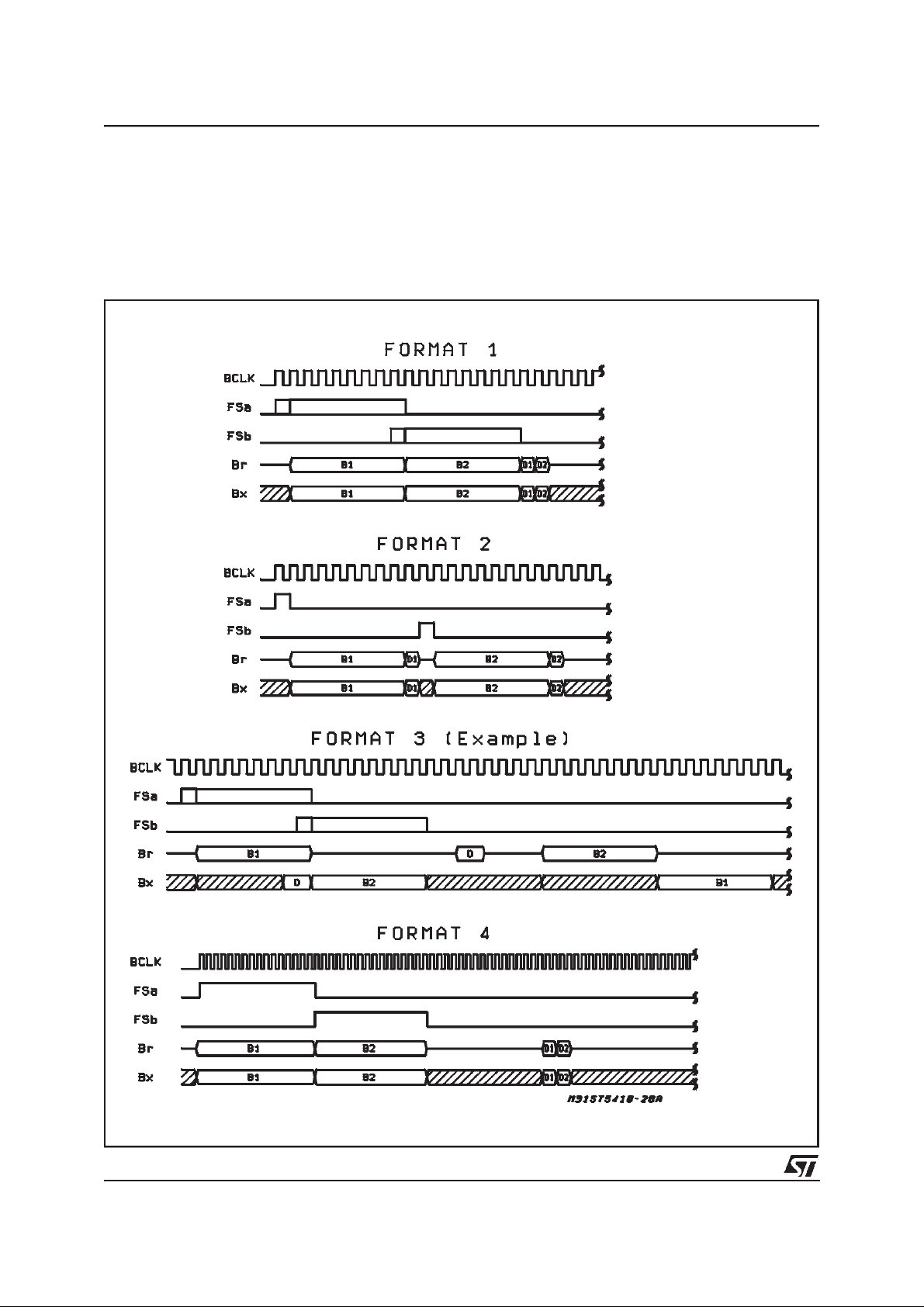
Format 1: the 2B+D data transfer is assignedto
the first18 bits of the frame on Br and Bx I/0 pins.
Channels are assigned as follows: B1(8 bits),
B2(8 bits), D(2 bits), with the remaining bits ignored until thenext Framesync pulse.
Format 2: the 2B+D data transfer is assignedto
the first 19 bits of the frame on Br and Bx I/O
pins. Channels are assigned as follows: B1(8
bits), D(1 bit), 1 bit ignored, B2(8 bits), D(1 bit),
with the remaining bits ignored until the next
frame sync pulse.
Format 3: B1 and B2 Channels can be independently assigned to any 8 bits wide time slot
among 64 (or less) on the Bx and Br pins. The
transmit and receive directions are also independent. When TDM mode is selected, the D
channel can be assigned to any 2 bits wide time
slot among 256 on the Bx and Br pins or on the
Dx and Dr pins (D port disabled or enabled in
TDM mode respectively).
Format 4: is a GCI like format excluding Monitor
channel and C/I channel.The 2B+D data transfer
is assigned to the first 26 bits of the frame on Br
and Bx I/O pins. Channels are assigned as follows. B1(8 bits) B2(8 bits), 8 bits ignored, D(2
bits), with remaining bits ignored up to the next
frame syncpulse.
When the Digital Interface clocks are selected as
inputs, FSa must be a 8 kHz clock input which indicates the start of the frame on the data input pin
Bx. When the Digital Interface clocks are selected
as outputs, FSa is an 8 kHz output pulse conforming to the selected format which indicates
the frame beginning for both Tx and Rx directions.
When the Digital Interface clocks are selected as
inputs, FSb is a 8 kHz clock input which defines
the start of the frame on the data ouput pin Br.
When the Digital Interface clocks are selected as
outputs, FSb is a 8 kHz output pulse indicating
the second 64kbit/s slot.
Two phase-relations between the rising edge of
FSa/FSb and the first (or second for FSb as output) slot of the frame can be selected depending
on format selected: Delayed timing mode or non
Delayed timing mode.
Non delayed data mode is similar to long frame
timing on the COMBOI/II series of devices: The
first bit of the frame begins nominally coincident
with the rising edge of FSa/b. When output, FSa
is coincident with the first 8 bits wide time-slot
while FSb is coincident with the second 8 bits
wide time-slot. Non delayed mode is not available
in format 2.
Delayed timing mode, which is similar to short
frame sync timing on COMBO I/II, in which the
FSa/b input must be set high at least a half cycle
of BCLK earlier the frame beginning. When output, FSa 1bit wide pulse indicates the first 8 bits
wide time-slot while FSb indicates the second.
Delayed mode is not availablein format4.
2B+D basic access data to transmit to the line
can be shifted in at the BCLK frequency on the
falling edges during the assigned time-slots.
When D channel port is enabled, only B1 & B2
data is shiftedin duringthe assigned time slots. In
format 4, data is shifted in at half the BCLK frequencyon the receive fallingedges.
2B+ D basic access data received from the line
can be shiftedout from the Br output at the BCLK
frequencyon the rising edges during the assigned
time-slots.Elsewhere,Br is in thehigh impedance
state. When the D channel port is enabled, only
B1 & B2 data is shiftedout from Br. In Format 4,
data is shifted out at half the BCLK frequency on
the transmit rising edges; there is 1.5 period delay
between the rising transmit edge and the receive
falling edge of BCLK.
15/74
STLC5412
Bit Clock BCLK determines the data shift rate on
the Digital Interface. Depending on mode selected, BCLK is an input which may be any multiple of 8 kHz from 256 kHz to 6176 kHz or an output at a frequency depending on the format and
the frequency selected. Possible frequenciesare:
256 KHz, 512 KHz, 1536 KHz,
Figure 2: DSI Interfaceformats:MASTER mode.
2048KHz, 2560 KHz.
In format 4 the use of 256kHzis forbidden.
BCLK is synchronouswith FSa/b frame sync sig-
nal. When output, BCLK is phased locked to the
recoveredclock receivedfrom the line.
16/74
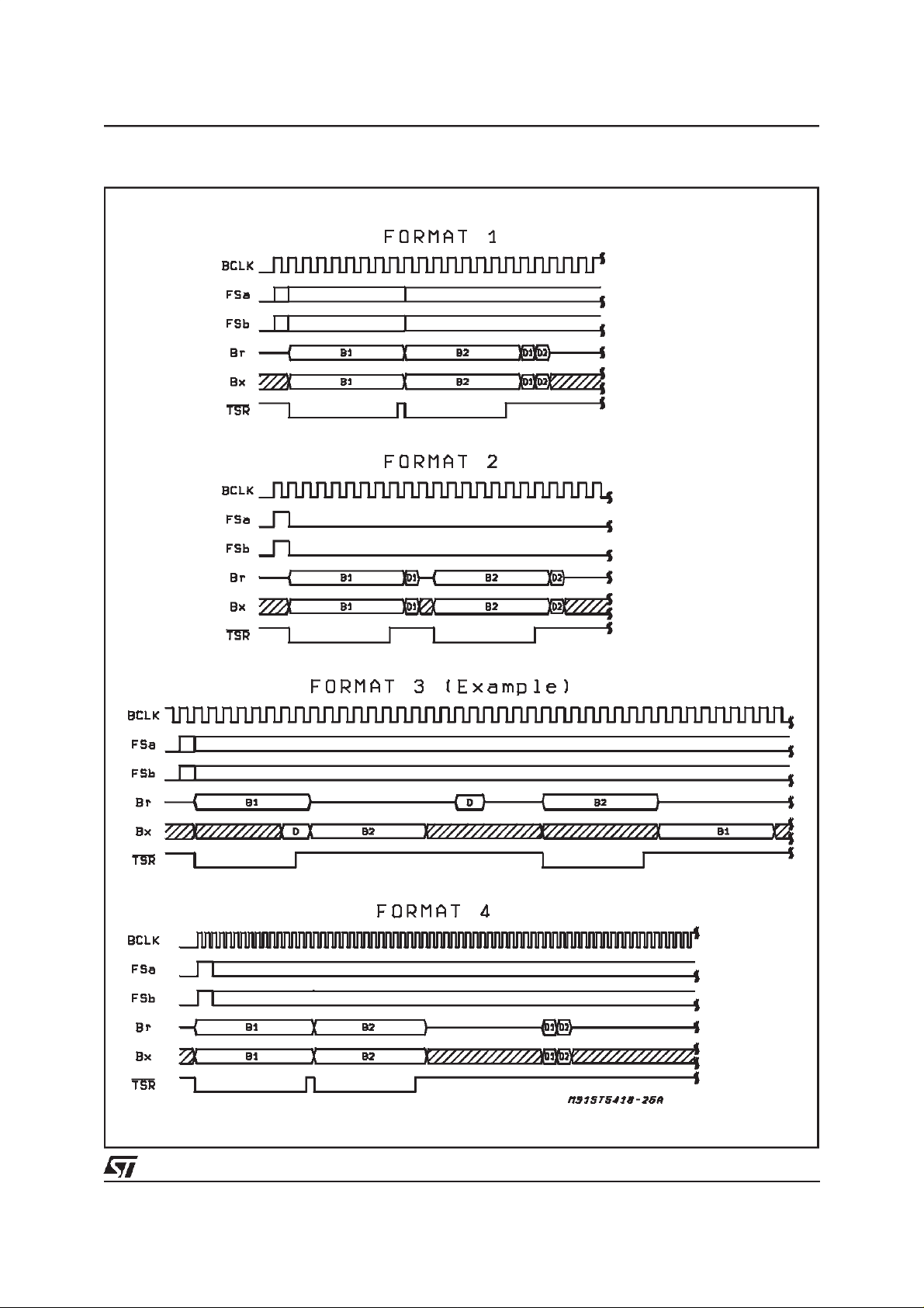
Figure 3: DSI Interfaceformats:SLAVE mode.
STLC5412
17/74
STLC5412
GCI MODE
The GCI is a standard interface for the interconnection of dedicated ISDN componentsin the different equipments of the subscriberloop:
In a Terminal, GCI interlinks the STLC5412, the
ISDN layer 2 (LAPD) controllerand the voice/data
processing componentsas an audio-processoror
a TerminalAdaptormodule.
In NT1-2, PABX subscriber line card, or central
office line card (LT), GCI interlinks the UID, the
ISDN Layer 2 (LAPD) controllers and eventually
the backplane where the channels are multiplexed.
In NT1, GCI interlinks SID-GCI and STLC5412,
via automode (NT1-auto). In Regenerators, GCI
links both STLC5412 UID in automode (NT-RRauto, LT-RR-auto). (See Fig. 4a)
Frame Structure
2B+D data and control interface is transferredin a
time-division multiplexed mode based on 8 kHz
frame structure and assigned to four octets per
frame and direction.(seefig.4b).
The 64 kbit/s channels B1 and B2 are conveyed
in the first two octets; the third octet (M: Monitor)
is used for transferring most of the control and
status registers;the fourth octet (SC: Signalling &
Control) contains the two D channel bits, the four
C/I (command/lndicate)bits controlling the activation/deactivation procedures, and the E & A bits
which support the handling of the Monitor channel.
Figure 4a: GCIconfigurationsof the UID.
These four octets per frame serving one ISDN
subscribers line form a GCI Channel. One GCI
channel calls for a bit rate of 256 kbit/s.
In NT1-2s or subscriber Line Cards up to 8 GCI
channels may be carried in a frame of a GCI multiplex. The bit rate of a GCImultiplex may be from
256 kbit/s and up to 3088 kbit/s. Adjacent 4-octet
slots from the frame start are numbered 0 to 7.
The GCI channel takes the number of the slot it
occupies.Spare bits in the frame beyond 256 bits
from the frame start will be ignored by GCI compatible devices but may be used for other purposes if required (see Fig.4c). GCI channel number is selectedby biasing pins S0,S1,S2.
Physical Links
Four physical links are usedin the GCI.
Transmitteddata to the line: Bx
Receiveddata from the line: Br
Data clock: BCLK
Frame Synchronizationclock: FSa
GCI is always synchronized by frame and data
clocks derived by any masterclock source.
A device used in NT mode can deliver clock
sources able to synchronize GCI, either directly,
or via a local Clock Generator synchronized on
the line by means of the SCLK 15.36 MHz output
clock. Frame clock and data clock could be independent of the internal devices clocks. Logical
one on the Br output is the high impedance state
while logical zero is low voltage. For E and A bits,
active state is voltage Low while inactive state is
high impedancestate.
Figure 4a: GCI configurations of the UID
TERMINAL
18/74
NT1 REPETOR
NT
PRIVATETERMINAL
OR NT1-2
U
LTNT-RR-AUTOLT-RR-AUTONT1-AUTOSID-GCISID-GCI
LINE TERMINATIONSU U
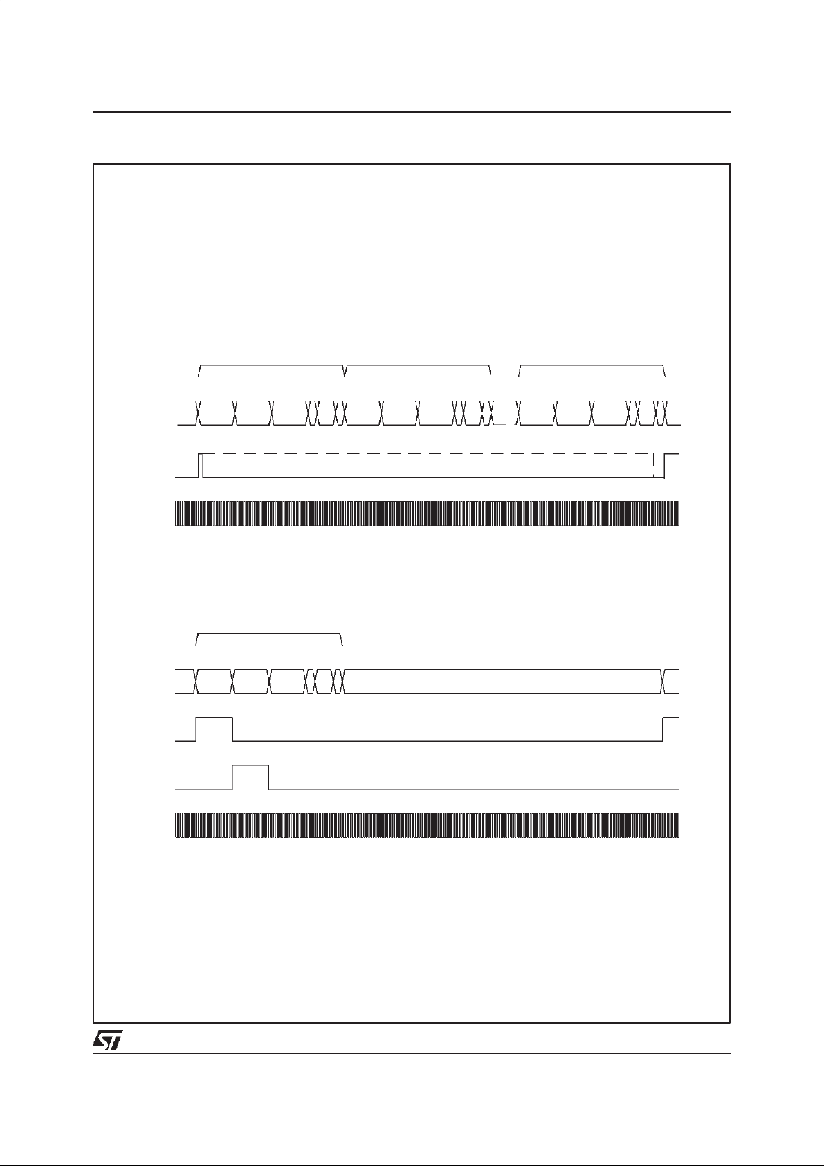
Figure 4b: GCI interfaceformat.
STLC5412
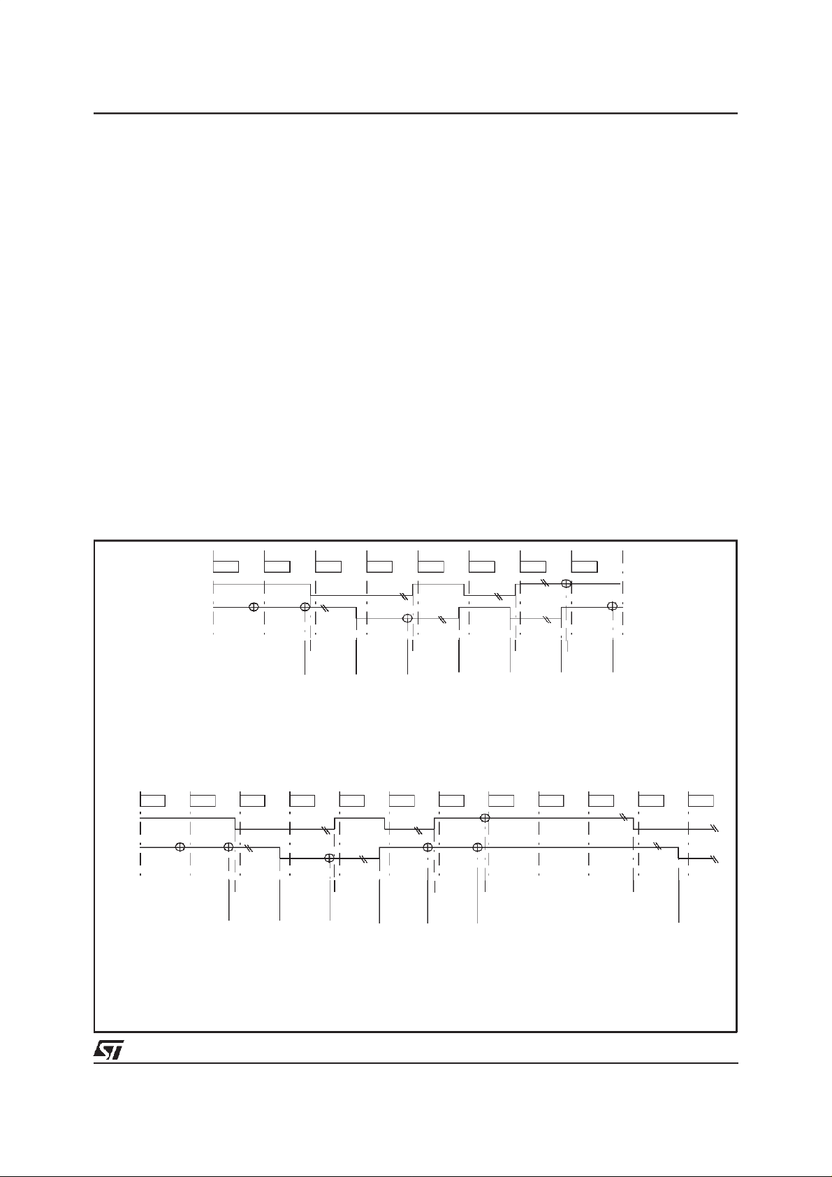
Figure 4b:
Bx/Br
FSa
BCLK
Bx/Br
GCI interface format
GCI CHANNEL 0 GCI CHANNEL 1 GCI CHANNEL 7
B1 B2 M D C/I A E
88 8242
8 KHz
GCI CHANNEL 0
B1 B2 M D C/I A E
8 8 8 242
B1 B2 M D C/I A E
88 8242
SLAVE MODE
FREE
B1 B2 M D C/I A E
88 8242
FSa
FSb
BCLK
8 KHz
MASTER MODE (BCLK = 1.536MHz)
MASTER MODE
19/74

STLC5412
Figure 4c: GCImultiplexexamples,(slavemode).
20/74
STLC5412
Data is transmitted in both directions at half the
data clock rate. The information is clocked by the
transmitteron the front edge of the data clockand
can be accepted by the receiver after 1 to 1.5 period of the data clock.
The data clock (BCLK) is a square wave signal at
twice the data transmission frequency on Bx and
Br with a 1 to 1 duty cycle. The frequencycan be
choosen from 512 to 6176 kHz with 16 kHz
modularity. Data transmission rate depends only
on the data clock rate.
The Frame Clock FSa is a 8 kHz signal for synchronization of data transmission. The front edge
of this signal gives the time reference of the first
bit in the first GCI input and output channel, and
resetthe slot counterat the startof each frame.
When some GCI channels are not selected on
devices connected to the same GCI link, these
time slots are free for alternativeuses.
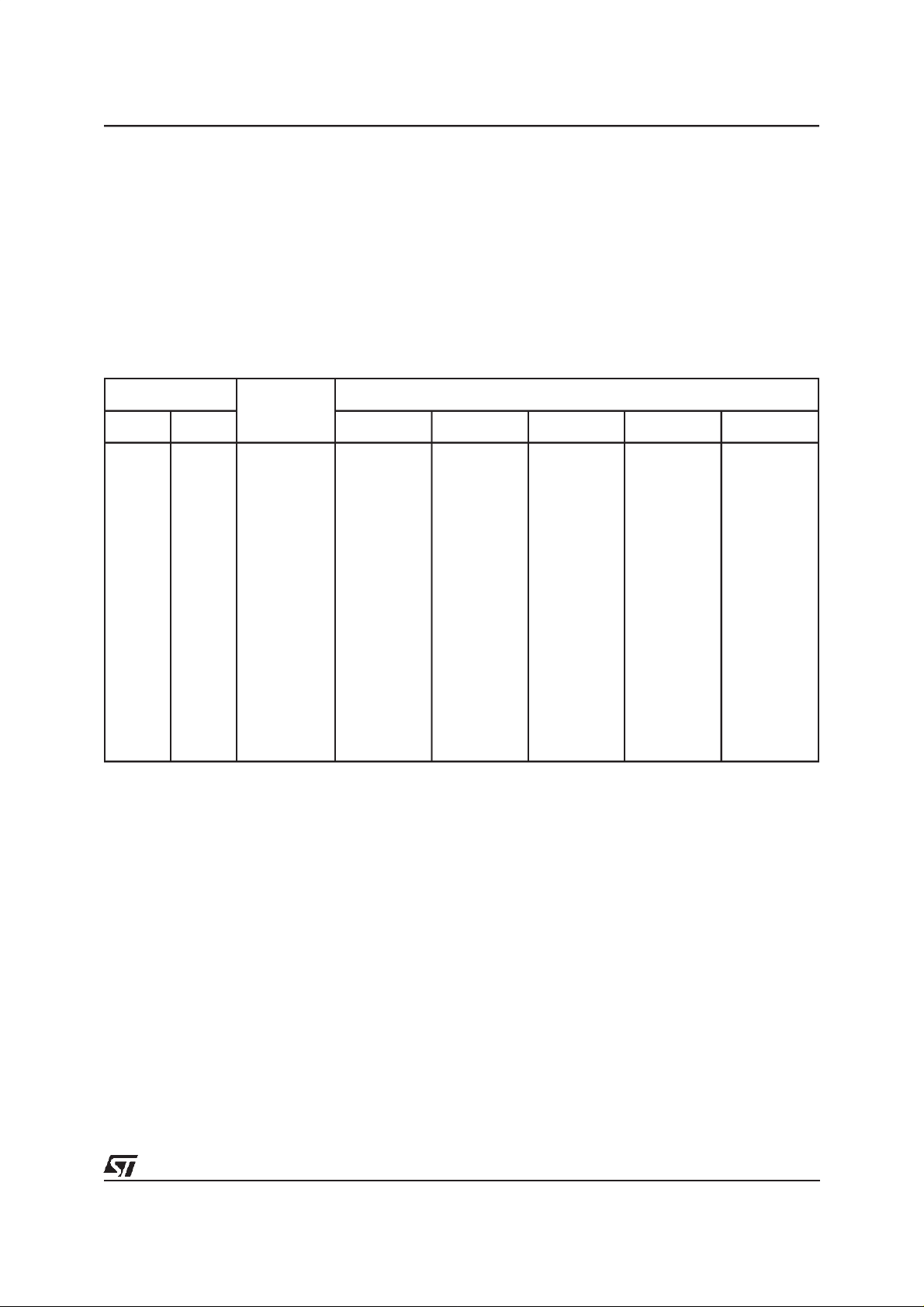
GCI configuration selection is done by biasing of
input pins MW, M0, CONF1,CONF2 according to
Table1.
Table 1: GCIConfigurationselection.
Pin Number
PLCC44 DIP28 LT/NT12 (1) NT/TE NT1-AUTO LT-RR-AUTO NT-RR-AUTO
4328MW00000
4227M001111
27 19 S1/CONF1 S1 0 1 1 0
25 17 S2/CONF2 S2 1 1 0 0
10 7 S0/FSb/TEST2 S0 FSb TEST2 TEST2 TEST2
Pin name
Configuration
26 18 IO1/ES1 (2) IO1 IO1 ES1 PLDD ES1
24 16 IO2/ES2 (2) IO2 IO2 ES2 EC ES2
23 15 IO3/EC (2) IO3 IO3 EC LFS LFS
22 14 IO4/TEST1 (2) IO4 IO4 TEST1 TEST1 TEST1
35 22 SFSx/RFS (2) SFSx SFSx SFSx RFS RFS
(1) Differentationbetween LTand NT configurationdone by bit NTS in CR2 register;GCIin slave mode.
When NT1-AUTO or NT-RR-AUTO configuration is selected, BCLK bit clock frequency of 512 kHz is
automaticallyselected
When NT configurationis selected,BCLK bit clock frequencyof 1536 kHzis automaticallyselected.
(2) Connectedto V
throughinternal pull-upresistors.
CC
21/74
STLC5412
Monitor channel
The Monitor channel is used to write and read all
STLC5412 internal registers. Protocol on the
Monitor channel allows a bidirectional transfer of
bytes between UID and a control unit with acknowledgement at each received byte. Bytes are
transmitted on the Br output and received on the
Bx input in theMonitorchanneltime slot.
A write or read cycle is always constituted of two
bytes.(see fig. 5). It is possible to operate several
write or read cycles within a single monitor message.
Note: Special format is used for EOC channel.
Write cycle
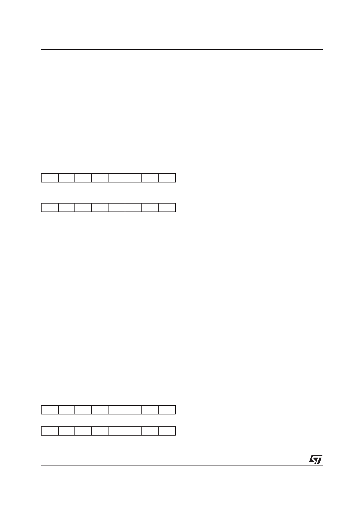
The format to write a messageinto theUID is:
A7 A6 A5 A4 A3 A2 A1 A0
1st byte
D7 D6 D5 D4 D3 D2 D1 D0
2nd byte
A7-A1:
A0:
D7-D0:
RegisterAddress
Write/Readback Indicator
RegisterContent
After the first byte is shifted in, Register address
is decoded. A0 set low indicates a write cycle: the
content of the following received byte has to be
loaded intothe addressedregister.
A0 set high indicates a read-back cycle request.
The second byte content is not significative.
STLC5412 will respond to the request by sending
back a message with the register content associated with its own address. It is then possible for
the microprocessor to receive the required register content after several other pendingmessages.
To avoid any loss of data, it is recommended to
operate only one read-backrequestat a time.
Note: Special format is used for EOC channel.
Read cycle
When UID has a register content to send to the
controller, it send it on the monitor channel directly. Note that the data to send can be the content of a Register previously requested by the
controllerby meansof a read-backrequest.
The format of the messagesent by the UID is:
A7 A6 A5 A4 A3 A2 A1 A0
1st byte
D7 D6 D5 D4 D3 D2 D1 D0
2nd byte
A7-A1:
A0:
RegisterAddress
forced to 0 if spontaneous
interrupt,forcedto 1 if readback
D7-D0:
RegisterContent
ExchangeProtocol
STLC5412 validates a received byte if it is detectedtwo consecutive times identical.(see fig. 5)
The exchange protocol is identical for both directions. The sender uses the E bit to indicate that it
is sending a Monitor byte while the receiver uses
A bit to acknowledge the received byte.When no
message is transferred,E bit and A bit are forced
to inactive state.
A transmission is started by the sender (Transmit
section of the Monitor channel protocol handler)
by putting the E bit from inactive to active state
and by sending the first byte on Monitor channel
in the same frame. Transmission of a message is
allowed only if A bit sent from the receiver has
been set inactive for at least two consecutive
frames. When the receiver is ready, it validates
the incoming byte when received identical in two
consecutive frames. Then, the receiver set A bit
from the inactive to the active state (preacknowledgement) and maintain active at least in the followingframe (acknowledgement).
If validation is not possible (two last bytes received are not identical) the receiver aborts the
message by setting the A bit active for only a single frame.The second byte can be transmitted by
the sender putting the E bit from the active to the
inactivestate and sending the second byte on the
Monitor channel in the same frame . The E bit is
set inactive for only one frame. If it remains inactive more than one frame, it is an end of message. The second byte may be transmittedonly
after receiving of the pre-acknowledgementof the
previous byte . Each byte hasto be transmittedat
leastin two consecutiveframes.
The receiver validates the current received byte
as for the first one and then set the A bit in the
next two frames first from the active state to the
inactivestate (pre-acknowledgement)and back to
the active (acknowledgement).If the receivercannot validates the received current byte (two bytes
received not identical)it pre-acknowledges normally but let the A bit in the inactive state in the
next frame which indicates an abort request . If a
message sent by the UID is aborted,the UID will
send again the complete message until receiving
of an acknowledgement . A message received by
the UID can be acknowledged or aborted with
flow Control.
The most significant bit (MSB) of Monitor byte is
sent first on the Monitor channel. E & A bits are
active low and inactive state on Br is 5 V. When
no byte is transmitted, Monitor channel time slot
22/74
STLC5412
on Br is in the high impedance state.
A 24 ms timer is implemented in the UID. This
timer (when enabled) starts each time the sender
starts a byte sending and waits for a pre acknowledgement.
C/I channel
The C/I channel is used for TXACT and RXACT
registers write and read operation. However, it is
possible to access to ACT registers by monitor
channel: this access is controled by the CID bit in
CR2 register.
The four bits code (C1,C2,C3,C4) of TXACT register can be loaded in the UID by writing permanently this code in the C/I channel time-slot on Bx
input every GCI frames. The UID takes into account the received code when it has been received two consecutive times identical. When a
status change occurs in the RXACT register, the
new (C1,C2,C3,C4) code is sent in the C/I channel time-slot on Br output every GCI frames. This
code is sent permanently by the UID until a new
status change occurs in RXACTregister.
C1 bit is sent first to the line.
Figure 5: GCI Monitor channelmessaging examples.
LINE CODING AND FRAME FORMAT
2B1Q coding rule requires that binary data bits
are grouped in pairs so called quats (see Tab.2).
Each quat is transmitted as a symbol, the magnitude of which may be 1 out 4 equallyspaced voltage levels (see Fig. 6). +3 quat refers to the
nominal pulse waveform specified in the ANSI
standard. Other quats are deduced directly with
respect of the ratio and keeping of thewaveform.
The frameformatused in UID follows ANSI specification (see Tab. 3 and 4). Each complete frame
consists of 120 quats, with a line baud rate of 80
kbaud, giving a frame duration of 1.5ms. A nine
quats lenght sync-word defines the framing
boundary. Furthermore,a Multiframeconsistingof
8 frames is defined in order to provide sub-channels within the spare bits M1 to M6. Inversion of
the syncword defines the multiframe boundary. In
LT, the transmit multiframe starting time may be
synchronizedby meansof a 12 ms period of time
pulse on the SFSx pin selected as an input (bit
SFS in CR2); If SFSx is selected as an output,
SFSx provides a square wave signal with the rising edge indicatingthe multiframe startingtime.
In NT, the transmit multiframe starting time is pro-
Tx M
Tx
Tx E
Tx
Rx A
Rx
XM1
Tx
Tx M
Tx E
Tx
Rx A
Rx
fora message
XM1M1
1st byte
(M1)
Ready for
a message
pre-ack ack
(M1) (M1)
TWO BYTES MESSAGE ABORTED ON THE SECOND AND RETRANSMITTED
M1 M2 M2
1st byte
(M1)
pre-ack ack
(M1)
TWO BYTES MESSAGE- NORMAL TRANSMISSION
M2 M2
2nd byte
(M2)
2nd byte
(M2)
(M1)
X
pre-ack abort
(M2) (M2)
E & A BITS TIMING
pre-ack ack
(M2) (M2)
XX
3rd byte??
(X)
Ready for
retransmission
XXX
3rdbyte??
(X)
EOM
(or abort ack)
EOM
pre-ack??
(X)
X
Ready forReady
M1 M1 M2
1st byte
(M1)
pre-ack
(M1)
23/74
 Loading...