

SGS Thomson Microelectronics STLC5411FN, STLC5411P Datasheet
GENERALFEATURES
SINGLE CHIP 2B1Q LINE CODE TRANSCEIVER
SUITABLEFOR BOTH ISDN AND PAIR GAIN
APPLICATIONS
MEETS OR EXCEEDS ANSI U.S. AND ETSI
EUROPEAN STANDARD
SINGLE 5V SUPPLY
DIP28AND PLCC44 PACKAGE
HCMOS3A SGS-THOMSON ADVANCED
1.2µm DOUBLE-METALCMOS PROCESS
STLC5411
2B1Q U INTERFACE DEVICE
PLCC44
TRANSMISSION FEATURES
160 KBIT/S FULLDUPLEX TRANSCEIVER
2B1Q LINE CODING WITH SCRAMBLER/DE-
SCRAMBLER
18KFT (5.5KM) ON 26AWG/24AWG
TWISTED PAIR CABLES
SUPPORTS BRIDGE TAPS, SPLICES AND
MIXED GAUGES
>70DBADAPTIVEECHO-CANCELLATION
ONCHIP HYBRIDCIRCUIT
DECISIONFEEDBACKEQUALIZATION
ONCHIP ANALOG VCOSYSTEM
DIRECT CONNECTION TO SMALL LINE
TRANSFORMER
SYSTEMFEATURES
ACTIVATION/DEACTIVATIONCONTROLLER
ON CHIP CRC CALCULATION AND VERIFI-
CATION INCLUDING TWO PROGRAMMABLE BLOCK ERRORCOUNTERS
EOC CHANNEL AND OVERHEAD-BITS
TRANSMISSION WITH AUTOMATIC MESSAGECHECKING
GCI AND MW/DSI MODULE INTERFACES
COMPATIBLE
DIGITAL LOOPBACKS
COMPLETE(2B+ D )ANALOGLOOPBACKINLT
ELASTIC DATA BUFFERS AND BACKPLANE
CLOCKDE-JITTERIZER
AUTOMODE NT1 AND REPEATER
”U ACTIVATIONONLY” IN NT1
IDENTIFICATION CODE AS PER GCI
STANDARD
ORDERING NUMBER: STLC5411FN
Plastic DIP28
ORDERING NUMBER: STLC5411P
EASILY INTERFACEABLE WITH ST5451
(HDLC & GCI CONTROLLER), ST5421 SIDGCI TRANSCEIVER AND ANY OTHER GCI,
IDL or TDMCOMPATIBLEDEVICES
November 1996
1/72

STLC5411
INDEX
DISTINCTIVECHARACTERISTICS .......................................... Page 1
GENERALDESCRIPTION ....................................................... 5
PIN FUNCTION ................................................................ 6
FUNCTIONAL DESCRIPTION.................................................... 14
Digital Interfaces . . . . .....................................................
µW/DSI mode . . . . . . . . . . . . . . . . . . . . . . . . . . . . . . . . . . . . . . . . ...................
µW Control Interface. . . . . . . . . . . . . . . . . . . . . . . ...............................
WriteCycle . . . . . . . . ..............................................
ReadCycle.........................................................1414
Digital System Interface. . . . . . . . . . . . . . . . ...................................
GCImode............................................................1518
Frame structure. . . . . ..............................................
Physicallinks . . . . . . . . . . . . . . . . . . . . . . . . . . . . . . . . . . . . . . . .. . . . . . . .. . . . .
Monitorchannel . . .................................................
C/I channel.. . . ...................................................
Line coding and frame format. . . . . . . . . . . . . . . . . .. . . . . . . . ....................
Transmitsection. . . . . . . . . . . . .............................................
Receivesection..........................................................
Elasticbuffers............................................................
Maintenancefunctions.. . . . . . . . . . . ........................................ 25
M channel.. . . . . . . . . . . . . . . . . . ....................................
EOC.............................................................
M4channel.......................................................
SpareM5andM6bits...............................................
CRC calculation checking. . . . . . . . . ................................. .
Loopbacks. . . . . . . . . . . . . . . . . . . . ..................................
Identificationcode. . .....................................................
GeneralpurposeI/Os......................................................
Testfunctions............................................................
14
14
14
18
18
22
23
24
24
24
25
25
25
25
26
26
26
33
33
34
Turningonandoffthedevice................................................
Poweron initialization. ...................................... ......
Line activationrequest. . . . . . . . . . . . . . . . . . . . . ........................
Powerup control. . . . . . . . . . . . . . . . . . . . . . . . . . . . . . . . . . . . ........ ....
Powerdown control . . . . . . . . . . . . . . ................................
Powerup state. . . . . . . . . . . . . . . . . . . ......................... ......
Powerdown state . . . . . . . . . . . ......................... .............
Activationdeactivationsequencing.. . . . . . . . . . . . . . . ...........................
Case of restricted activation. . . . . . .........................................
Resetof activation / deactivationstate machine . . . . . . . . . . . . . . . . . . . . . . . . . . . .. . . .. .
Hardwarereset...........................................................
Quietmode..............................................................
Automode...............................................................
34
34
34
34
35
35
35
35
35
35
35
35
36
Command/Indication(C/I) codes.. . . . . . . . . . . . . . . . . . . . . . . . ...................
Internalregister description . . . . . . ............... ...........................3640
Line interface circuit . . . . . . ...............................................
Boardlayout . . . . . . . . . . . ................................................5353
APPENDIX A: STATE MATRIX ................................................... 58
APPENDIX B: ELECTRICAL PARAMETERS ........................................ 60
2/72
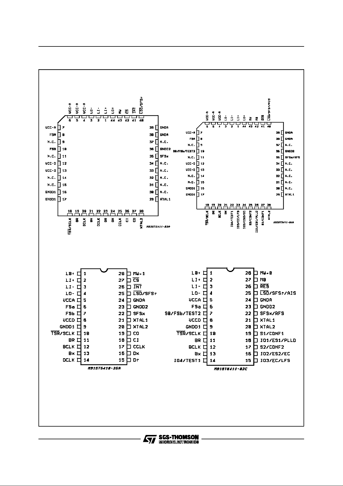
PIN CONNECTIONS (Top view)
STLC5411
PLCC44
MICROWIRE MODE
DIP28
PLCC44
GCI MODE
DIP28
MICROWIRE MODE
GCI MODE
3/72
STLC5411
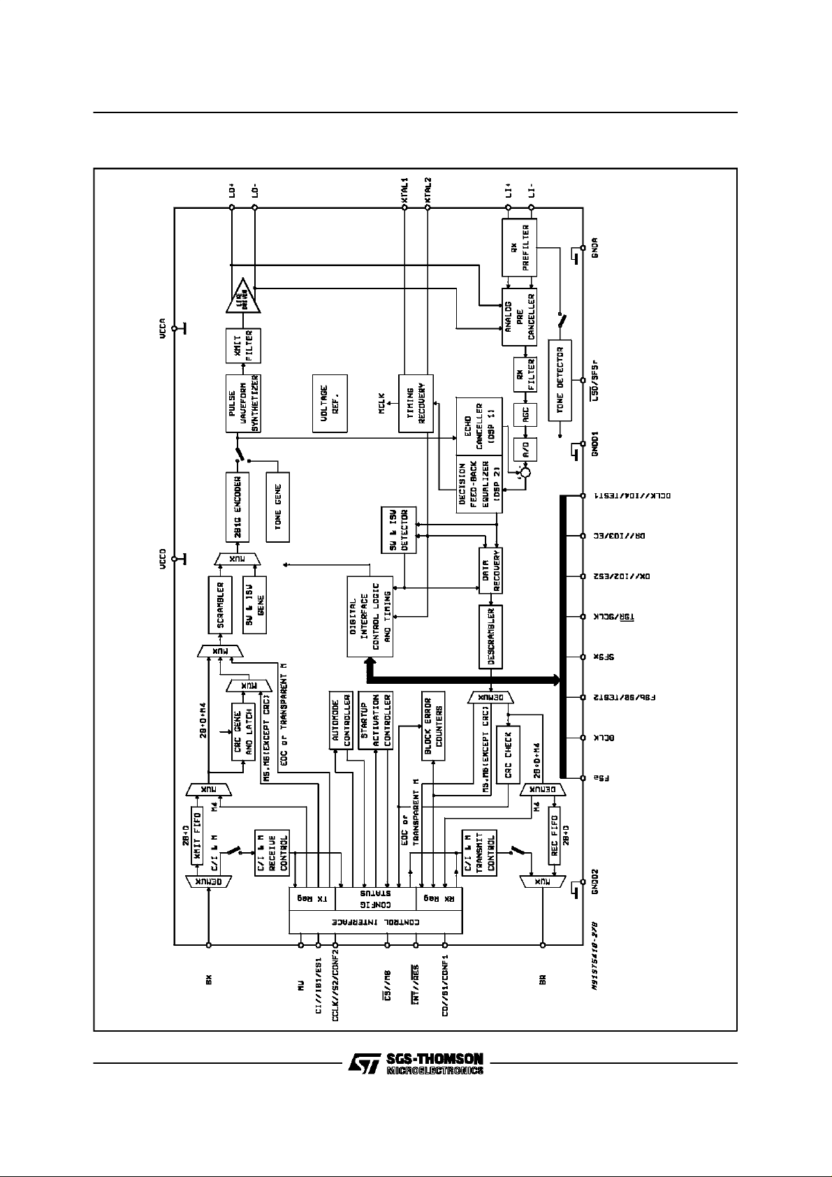
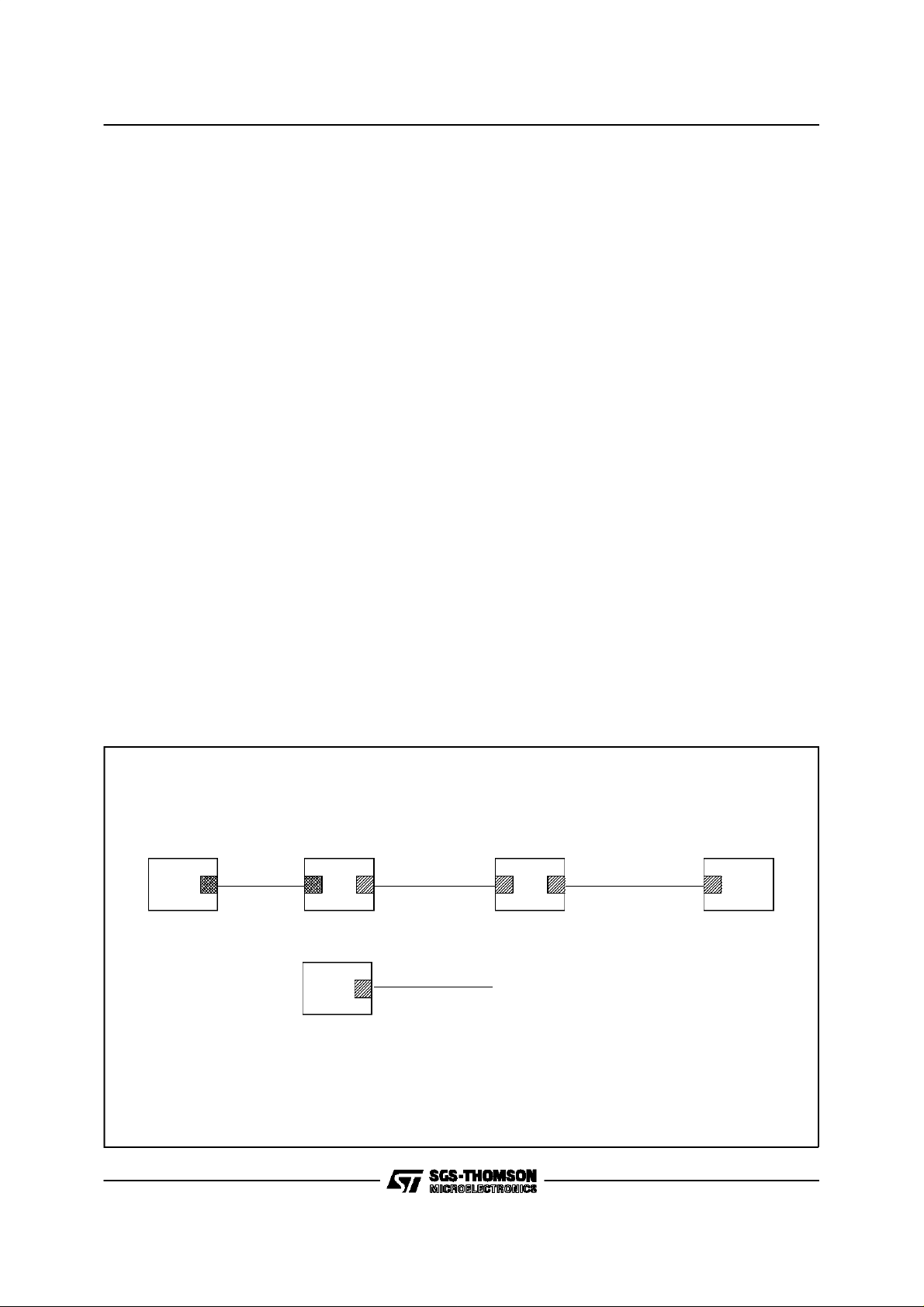
Figure1: BlockDiagram.
4/72

STLC5411
GENERALDESCRIPTION
STLC5411 is a complete monolithic transceiver
for ISDN Basic access data transmission on
twisted pair subscriber loops typical of public
switched telephone networks. The device is fully
compatiblewith both ANSI T1.601-1988U.S. and
CSE (C32-11) French specifications. It is intended also to comply with ETSI specification
bothin term of transmissionperformances and requested features.
The equivalent of 160 kbit/s full-duplex transmission on a single twisted pair is provided, according to the formats defined in the a.m. spec.
Framesinclude two B channels,each of 64 kbit/s,
one D channel of 16 kbit/s plus an additional 4
kbit/s M channel for loop maintenance and other
user functions. 12 kbit/s bandwidthis reserved for
framing.2B1Q Line codingis used, wherepairs of
bits are coded into one of 4 quantumlevels. This
technique results in a low frequency spectrum
(160 kbit/s turn into 80 kband), thereby reducing
both line attenuation and crosstalk and achieving
long range with low Bit ErrorRates.
The system is designed to operate on standard
types of cable pairs including mixed gauges (26
AWG, 24 AWG and 22 AWG) including the 15
loops configuration specified by ANSI. Good
noise margins are achieved even when bridged
taps are present. On 26 AWG cable, the transmission range is in excess of 5.5 km (18 kft) in
presence of crosstalk and noise as specified by
ANSI standard.STLC5411 is designed to operate
with Bit Error Rate near-end Crosstalk (NEXT) as
specifiedin europeanETSI recommendation.
To meet these very demanding specifications, the
device includes two Digital Signal Processors,
one configured as an adaptive Echo-Canceller to
cancel the near end echoes resulting from the
transmit/receive hybrid interface, the other as an
adaptive line equalizer. A Digital Phase-Locked
Loop (DPLL) timing recovery circuit is also included that provides in NT modes a 15.36 MHz
synchronized clock to the rest of the system.
Scrambling and descrambling are performed as
specifiedin the US and Frenchspecifications.
On the system side, STLC5411 can be linked to
twobus configuration simply by pin MW bias.
MICROWIRE(µW/DSI) mode (MWpin = 5V): 144
kbit/s 2B+D basic access data is transferred on a
multiplex Digital System Interface with 4 different
interface formats (see fig. 2 and 3) providing
maximum flexibility with a limited pin count
(BCLK, Bx, Br, FSa, FSb). Three pre-defined
2B+D formats plus an internal time slot assigner
allows direct connection of the UID to the most
common multiplexed digital interfaces (TDM/IDL).
Bit and Frame Synchronisation signals are inputs
or outputs depending on the configuration se-
lected. Data buffers allow any phase betweenthe
line and the digital interface. That permits building
of slave-slave configurations e.g. in NT12 trunkcards.
It is possible to separate the D from the B channels and to transfer it on a separate digital interface (Dx, Dr) using the same bit and frame clocks
as for the B channelsor in a continuousmode using an internallygenerated 16 kHz bit clock output
(DCLK).
All the Control, Status and Interrupt registers are
handled via a controlchannel on a separate serial
interface MICROWIRE compatible (CI, CO, CS,
CCLK, INT) supported by a number of microcontroller including the MCU families from SGSTHOMSON
GCI mode (MWpin = 0V). Control/maintenance
channels are multiplexedwith 2B+D basic access
data in a GCI compatibleinterface format (see fig.
4a) requiring only 4 pins (BCLK, Bx, Br, FSa). On
chip GCI channel assignementallows to multiplex
on thesame bus up to 8 GCI channels,each supporting data and controls of one device. Bit and
Frame Synchronisation signals can be inputs or
ouputs depending on the configuration selected.
Data buffers, again, allow to have any phase between the lineinterface and the digitalinterface.
Through the M channel and its protocol allowing
to check both direction exchanges, internal registers can be configured, the EOC channel and the
Overhead-bits can be monitored. Associated to
the M channel, there are A and E channels for
enabling the exchanged messages and to check
the flow control. The C/I channel allows the primitive exchangesfollowing the standard protocol.
In both mode (µW and GCI) CRC is calculated
and checkedin both directions internally.
In LT mode, the transmit superframe can be synchronized by an external signal (SFSx) or be self
running. In NT mode, the SFSx is always output
synchronizedby the transmitsuperframe.
Line side or Digital Interface side loopbacks can
be selected for each B1, B2 or D channel independently without restriction in transparent or in
non-transparent mode. A transparent complete
analog loopback allowing the test of the transmission path is also selectable.
Activation and deactivationprocedures,which are
automatically processed by UID, require only the
exchange of simple commands as Activation Request, Deactivation Request, Activation Indication. Cold and Warm start up proceduresare operated automatically without any special
instruction.
Four programmable I/Os are provided in GCI for
externaldevice control.
5/72
STLC5411
PIN FUNCTIONS (no SpecificMicrowire / GCIMode)
Note: all pin number are referred to PlasticDIP28 package.
Pin Name In/Out Description
1, 4 LO+, LO- Out, Out Transmit 2B1Q signaldifferential outputs to theline transformer. When
2, 3 LI+, LI- In, In Receive 2B1Q signal differential inputs from the line transformer.
5, 8 VCCA, VCCD In, In Positive power supply input for the analog and digital sections, which must
24,923GNDA,GNDD1
GNDD2
10 TSRb Out (LT configuration only)
SCLK Out (NT configuration only)
20 XTAL2 Out The output of the crystal oscillator, which should be connected to one end
21 XTAL1 In The master clock input, which requires either a parallel resonance crystal to
28 MW In MICROWIRE selection: When set high, MICROWIRE control interface is
In, In
In
used with an appropriate 1:1.5 step-up transformer and the proper line
interface circuit the linesignal conforms to the output specifications in ANSI
standard with anominal pulse amplitude of 2.5 Volts.
be +5 Volts +/-5% and must be directlyconnected together.
Negative power supply pins, which must be connected together close to
the device.
All digitaland analog signals are referred to these pins, whichare normally
at the system Ground.
This pin is an open drainoutput normally in the high impedance state which
pulls low when B1 and B2 time-slots are active. It can be used to enable the
Tristate control of a backplane line-driver.
15.36 MHz clock output which is frequency locked to the received line
signal activeas soon as UID is powered up except in NT1 Auto
configuration (active only if S line activation is requested)
of the crystal, if used. Otherwise, this pin must be left not connected.
be tied between this pin and XTAL2, or a logic level clock input from a
stable source. This clock does not need tobe synchronized to the digital
interface clocks (FSa, BCLK).Crystal specifications: 15.36 MHz +/-50ppm
parallel resonant; Rs ≤ 20 ohms; load with 33pF to GND each side.
selected. When set low, GCI interface is selected.
PIN FUNCTIONS (specific Micro Wire mode)
Pin Name In/Out Description
6 FSa In Out Input or Outputdepending of the CMS bitin CR1 register, FSa is a 8 KHz
7 FSb In Out Input or Outputdepending of the CMS bitin CR1 register, FSb is a 8 KHz
11 Br Out 2B+D datas tristate output. Datas received from the line are shifted out on
6/72
clock which indicates the start of the frame on Bx when FSa is input, or Bx
and Br when FSa is output.
Input or Output,the location of FSa relative to the frame on Bx orBx and Br
depens of DDM bit in CR1 register, also the selected format.
clock which indicates the start of the frame on Br when it is an input. When
it is an output, FSb is a 8 KHz pulse conforming with the selected format
and always indicatingthe second 64Kbit/sec channel of the frame on Br.
Input or Output,the location of FSb relative to the frame on Br depends of
DDM bit in CR1 register, also the selected format.
the rising edge (at the BCLK frequencyor the half BCLK frequency if format
4 is selected) during the assigned time slot. Br is in high impedance state
outside the assignedtime slot and during the assigned time slot ofthe
channel if it is disabled.
When D channel portis enabled, only B1 B2 are on Br.
STLC5411
PIN FUNCTIONS (specific Micro Wire mode)
Pin Name In/Out Description
12 BCLK In Out Bit clock input or output depending of the CMS bit in CMR register. When
13 Bx In 2B+D input. Basic access data to transmit to the line is shifted in on the
14 DCLK Out D channel clock output when the D channel port is enabled in continuous
15 Dr Out D channel data output when theD channel portis enabled. D channel data is
16 Dx In D channel data inputwhen the D channel port is enabled. D channel data is
17 CCLK In ClockinputfortheMICROWIREcontrolchannel: data is shiftedin and outon
18 CI In MICROWIRE control channel serial input: Two bytes data is shifted out the
19 CO Out MICROWIRE control channel: serial output: two bytes data is shifted out the
22 SFSx In Out Tx Super frame synchronization. The rising edgeof SFSxindicates the
25 SFSr Out Rx Super frame synchronization. The rising edge of SFSr indicates the
LSDb Out Line Signal Detect output (default conf.): This pin is an open drain output
26 INTb Out Interrupt output: Latched open-drain output signal which isnormally high
27 CS In Chip Select input: When this pin is pulled low, data can be shifted in and out
BCLK is an input, its frequency may be any multiple of 8 KHz from 256 KHz
to 4096 KHz in formats 1, 2, 3; 512 KHz to 6176 KHz in format 4. When
BCLK is an output, its frequency is 256 KHz, 512 KHz, 1536 KHz, 2048
KHz or 2560 KHz depending of the selection in CR1 register. In this case,
BCLK is locked to the recovered clock received from the line. Input or
Output BCLK is synchronous with FSa/FSb. Datas are shifted in and out (on
Bx and Br) at the BCLK frequency in formats1, 2, 3. In format 4 datas are
shifted out at half the BCLK frequency.
falling edges (at the BCLK frequency or the half BCLK frequency if format 4
is selected) during the assigned time-slots. When D channel port is
enabled, only B1 & B2 sampled on Bx.
mode. Datas are shifted in and out (on Dx and Dr) at 16 KHz on the falling
and rising edges of DCLK respectively. In master mode, DCLK is
synchronous with BCLK.
shifted out from the UID on thispinin 2 selectable modes: in TDM mode data
is shiftedout at the BCLKfrequency (orhalf BCLK frequency in format4) on
theridsing edgeswhentheassigned timeslot is active.In continuousmode
dataisshiftedout attheDCLK frequency on the risingedge continuously.
shifted infrom the UID on this pin in 2 selectable modes: in TDM mode data
is shifted in at the BCLK frequency (or half BCLK frequency in format 4) on
the falling edges when the assigned time slot is active. In continuous mode
data is shiftedout at the DCLK frequency on the fallingedge continuously.
CI and CO pins withCCLK frequency following2 modes. For each modethe
CCLKpolarity is indifferent. CCLK may be asynchronous with all the others
UID clocks.
UID on this pin on the rising or the falling edge of CCLK depending of the
working mode.
UID on this pin on the rising or the falling edge of CCLK depending of the
working mode. When not enabled by CS low, CO is high impedance.
beginning of thetransmit superframe on theline. In NT mode SFSxis always
an output. In LT mode SFSx is an input or an output depending of the SFSbit
in CR2 register. When SFSx is input,it must be synchronous of FSa.
begenning of the received superframe on the line. UID provides this output
only when ESFR bit in CR4 register is to 1.
which is normally in the high impedance state but pulls low when the device
previously in the power down state receives a wake-up by Tone from the
line. This signal is intended to be used to wake-up a micro-controller from a
low power idlemode. The LSD output goes back in the high impedance
state when the device is powered up.
impedance and goes low to request a read cycle. Pending interrupt datais
shiftedout from CO at thefollowing read-write cycle. Several pending interrupts
maybequeuedinternally and may provide severalinterrupt requests. INTis
freed uponreceiving ofCS lowandcan goes lowagain when CS is freed.
from the UID through CI & CO pins. When high, this pin inhibits the
MICROWIRE interface. For normal read or write operation, CS has to be
pulled low for 16 CCLK periods of time.
7/72
STLC5411
PIN FUNCTIONS (specific GCI mode)
Pin Name In/Out Description
6 FSa In Out Input or Outputdepending of the configuration. FSa is a 8 KHz clock which
7 FSb Out In NT/TE non auto-mode configuration, FSb is a 8 KHz pulse always
S0 In When MO = 0 (LT/NT12 configuration): S0 associated with S1 and S2
TEST2 In Input pin to select a transmission test in all auto mode configurations.
11 Br Out 2B+D and GCI control channel open drain output. Data is shifted out (at the
12 BCLK In Out Bit clock input or output depending of the configuration. When BCLK is an
13 Bx In 2B+D and GCI control channelinput. Data is sampled by the UID on the
14 IO4 In Out General purpose programmable I/O configured by CR5 register in all non
TEST1 In Input pin to select a transmission test in all auto mode configurations.
15 IO3 In Out General purpose programmable I/O configured by CR5 register in all non
EC Out External control output pin in NT1 auto configuration. Normaly high, this pin
LFS In Local febe select:
16 IO2 In, Out General purpose programmable I/O configured by CR5 register in all non
EC Out External control output pin in LTRR auto configuration. Normaly high, this
ES2 In External status input pin. In NT1 autoand NTRR auto configurations, this
17 S2 In When MO = 0 (LT/NT12 configuration): S2 associated with S0 and S1
CONF2 In When MO = 1: Configuration input pin. Is used associated with CONF1 to
18 IO1 In Out General purpose programmable I/O configured by CR5 register in all non
ES1 In External status input pin. In NT1 autoand NTRR auto configurations, this
PLLD In PLL1 can be disabled in LTRR onto configuration with this pin.
19 S1 In When MO = 0 (LT/NT12 configuration): S1 associated with S0 and S2
CONF1 In When MO = 1: Configuration input pin. Is used associated with CONF2 to
indicates the start of the frame onBx and Br.
indicating the second 64Kbit/sec channel of the frame on Br.
selects a GCI channel number on Bx/Br.
TEST2 is associated with TEST1.
half BCLK frequency) on the first rising edge of BCLK during the assigned
channels slot. Br is in highimpedance state outside the assigned time slot
and during the assigned time slot of a channel if it is disabled.
input, its frequency may be any multiple of 16 KHz from 512 KHz to 6176
KHz.. When BCLK is an output, its frequence is 512 KHz in NT1 auto and
NTRR auto configurations, 1536 KHz in NT/TE configuration; In this case,
BCLK is locked to the recovered clock received from the line. Input or
Output BCLK is synchronous with FSa. Datas are shifted in and out (on Bx
and Br) at the half the BCLK frequency.
second falling edge of BCLK within the period of the bit, during the assigned
channels time slot.
auto mode configurations.
TEST1 is associated with TEST2.
auto mode configurations.
is pulled low when an eoc message ”öperate 2B+D loopback” is recognized
from the line.
When tied to 1 the febe is locallylooped back. See figure 10.
auto mode configurations.
pin is pulled low when an ARL command is received by the UID.
status is sent on the line throughthe ps2 bit.
selects a GCI channel number on Bx/Br.
select configuration NT/TE (non auto), NT1 auto, LTRR auto and NTRR
auto.
auto mode configurations.
status is sent on the line throughthe ps1 bit.
selects a GCI channel number on Bx/Br.
select configuration NT/TE (non auto), NT1 auto, LTRR auto and NTRR
auto.
8/72

STLC5411
PIN FUNCTIONS (specific GCI mode)
Pin Name In/Out Description
22 RFS In Remote febe select:
25 AIS In Analog interface select for all auto mode configurations
SFSr Out Rx Super frame synchronization. The rising edge of SFSr indicates the
LSDb Out Line Signal Detect output (default conf.): This pin is an open drain output
26 RESb In Reset input pin with internal pull-up resistor. When pulled low, all registers
27 M0 In Configuration input pin. When pulled low, GCI channel assigner is selected
When tied to 0 the remote febe is not transferred. When tied to 1 febe is
transparently reported. Seefigure 10.
beginning of the received superframe on the line. UID provides this output
only when ESFR bit in CR4 register is to 1 and LT/NT12 or NT/TE
configuration is done.
which is normally in the high impedance state but pulls low when the device
previously in the power down state receives a wake-up by Tone from the
line. This signal is intended to be used to wake-up a micro-controller from a
low power idlemode. The LSD output goes back in the high impedance
state when the device is powered up.
of the UID are reset to their default values. UID is configuredaccording to
configuration inputs bias excluding MW input which must be maintained at
the 0 volt. minimum recommended pulse length is 200µs.
(channel number defined by inputs S0, S1, S2). When pulled high, UID is
configured by pins CONF1 and CONF2.
MULTIPLE FUNCTION PIN DESCRIPTION
Pin6: FSa
Function or In/Out conditions (*) Function In/Out
MW(pin) = 1
MW(pin) = 0
MO(pin) = 1
MO(pin) = 0 FSa In
CMS(cr1) = 1 FSa Out
CMS(cr1) = 0 FSa In
CONF2(pin) = 1
CONF2(pin) = 0
(*) Only true if ANATST (internal test signal) = 0
CONF1(pin) = 1 FSa Out
CONF1(pin) = 0 FSa Out
CONF1(pin) = 1 FSa In
CONF1(pin) = 0 FSa Out
9/72
STLC5411
MULTIPLE FUNCTION PIN DESCRIPTION
Pin7: S0/FSb/TEST2
Function or In/Out conditions (*) Function In/Out
MW(pin) = 1
MW(pin) = 0
MO(pin) = 1
MO(pin) = 0 S0 In
(*) Only true if ANATST (internal test signal) = 0
Pin10: TSR~/SCLK/TCLK
Function or In/Out conditions (*) Function In/Out
MW(pin) = 1
MO(pin) = 1
MW(pin) = 0
MO(pin) = 0
(*) Only true if TDSPANA (internal testsignal) = 0
CMS(cr1) = 1 FSb Out
CMS(cr1) = 0 FSb In
CONF2(pin) = 1
CONF2(pin) = 0
NTS(cr2) = 1 SCLK Out
NTS(cr2) = 0 TSR~ Out OD
CONF2(pin) = 1
CONF2(pin) = 0
NTS(cr2) = 1 SCLK Out
NTS(cr2) = 0 TSR~ Out OD
CONF1(pin) = 1 TEST2 In
CONF1(pin) = 0 FSb Out
CONF1(pin) = 1 TEST2 In
CONF1(pin) = 0 TEST2 Out
CONF1(pin) = 1 SCLK Out
CONF1(pin) = 0 SCLK Out
CONF1(pin) = 1 TSR~ Out OD
CONF1(pin) = 0 SCLK Out
Pin12: BCLK
MW(pin) = 1
MW(pin) = 0
10/72
Function or In/Out conditions Function In/Out
CMS(cr1) = 1 BCLK Out
CMS(cr1) = 0 BCLK In
CONF2(pin) = 1
MO(pin) = 1
CONF2(pin) = 0
MO(pin) = 0 BCLK In
CONF1(pin) = 1 BCLK Out
CONF1(pin) = 0 BCLK Out
CONF1(pin) = 1 BCLK In
CONF1(pin) = 0 BCLK Out
MULTIPLE FUNCTION PIN DESCRIPTION
Pin14: DCLK/IO4/TEST1/TSYNC[R+]
Function or In/Out conditions Function In/Out
MW(pin) = 1
MO(pin) = 1
MW(pin) = 0
MO(pin) = 0
DEN(cr2) = 1
DEN(cr2) = 0 TSYNC Out
CONF2(pin) = 1
CONF2(pin) = 0 TEST1 In
Pin15: Dr/IO3/EC/LFS/TDOUT[R+]
Function or In/Out conditions (*) Function In/Out
MW(pin) = 1
MO(pin) = 1
MW(pin) = 0
MO(pin) = 0
DEN(cr2) = 1 Dr Out
DEN(cr2) = 0 TDOUT Out
CONF2(pin) = 1
CONF2(pin) = 0 LFS In
(*) Only true if TDSPANA (internal testsignal) = 0
STLC5411
DMO(cr2) = 1 DCLK Out
DMO(cr2) = 0 TSYNC Out
CONF1(pin) = 1 TEST1 In
CONF1(pin) = 0
CONF1(pin) = 1 EC Out
CONF1(pin) = 0
IO4(cr5) = 1 I4 In
IO4(cr5) = 0 O4 Out
IO4(cr5) = 1 I4 In
IO4(cr5) = 0 O4 Out
IO3(cr5) = 1 I3 In
IO3(cr5) = 0 O3 Out
IO3(cr5) = 1 I3 In
IO3(cr5) = 0 O3 Out
Pin16: Dx/IO2/EC/ES2/TDIN[R+]
Function or In/Out conditions (*) Function In/Out
MW(pin) = 1
MO(pin) = 1
MW(pin) = 0
MO(pin) = 0
DEN(cr2) = 1 Dx In
DEN(cr2) = 0 TDIN In
CONF2(pin) = 1
CONF2(pin) = 0
(*) Only true if TGSCEN(internal test signal) = 0
CONF1(pin) = 1 ES2 In
CONF1(pin) = 0
CONF1(pin) = 1 EC Out
CONF1(pin) = 0 ES2 In
IO2(cr5) = 1 I2 In
IO2(cr5) = 0 O2 Out
IO2(cr5) = 1 I2 In
IO2(cr5) = 0 O2 Out
11/72

STLC5411
MULTIPLE FUNCTION PIN DESCRIPTION
Pin17: CCLK/S2/CONF2
Function or In/Out conditions Function In/Out
MW(pin) = 1 CCLK In
MW(pin) = 0
Pin18: CI/IO1/ES1/PLLD[R+]
MW(pin) = 1 CI In
MW(pin) = 0
Pin19: CO/S1/CONF1
MO(pin) = 1 CONF2 In
MO(pin) = 0 S2 In
Function or In/Out conditions Function In/Out
CONF1(pin) = 1 ES In
MO(pin) = 1
MO(pin) = 0
CONF2(pin) = 1
CONF2(pin) = 0
CONF1(pin) = 0
CONF1(pin) = 1 PLLD In
CONF1(pin) = 0 ES1 In
IO1(cr5) = 1 I1 In
IO1(cr5) = 0 O1 Out
IO1(cr5) = 1 I1 In
IO1(cr5) = 0 O1 Out
Function or In/Out conditions Function In/Out
MW(pin) = 1 CO Out
MW(pin) = 0
MO(pin) = 1 CONF1 In
MO(pin) = 0 S2 In
Pin22: SFSx/RFS [R+]
Function or In/Out conditions Function In/Out
NTS(cr2) = 1 SFSx Out
MW(pin) = 1
MW(pin) = 0
MO(pin) = 1
MO(pin) = 0
NTS(cr2) = 0
CONF2(pin) = 1 SFSx Out
CONF2(pin) = 0 RFS In
NTS(cr2) = 1 SFSx Out
NTS(cr2) = 0
SFS(cr2) = 1 SFSx Out
SFS(cr2) = 0 SFSx In
SFS(cr2) = 1 SFSx Out
SFS(cr2) = 0 SFSx In
12/72
STLC5411
MULTIPLE FUNCTION PIN DESCRIPTION
Pin25: LSD/SFSr/AIS
Function or In/Out conditions Function In/Out
MW(pin) = 1
CONF1(pin) = 1 AIS In
MO(pin) = 1
MW(pin) = 0
MO(pin) = 0
CONF2(pin) = 1
CONF2(pin) = 0 AIS In
CONF1(pin) = 0
Pin26: INT/RES [R+]
Function or In/Out conditions Function In/Out
MW(pin) = 1 INT Out OD
MW(pin) = 0 MO In
ESFR(cr4) = 1 SFSr Out OD
ESFR(cr4) = 0 LSD Out OD
ESFR(cr4) = 1 SFSr Out OD
ESFR(cr4) = 0 LSD Out OD
ESFR(cr4) = 1 SFSr Out OD
ESFR(cr4) = 0 LSD Out OD
Pin27: CS/MO
Function or In/Out conditions Function In/Out
MW(pin) = 1 CS In
MW(pin) = 0 MO In
PIN28: MW
Notes: [R+] = Pull up Resistor
: Out OD = Open Drain Output
13/72
STLC5411
FUNCTIONAL DESCRIPTION
DigitalInterfaces
STLC5411 provides a choice between two types
of digital interface for both control data and (2
B+D) basic accessdata.
Theseare:
a) GeneralCircuit Interface:GCI.
b) Microwire/DigitalSystem Interface:
µW/DSI
The device will automatically switch to one of
them by sensing the MW input pin at the Power
up.
µW/DSI MODE
Microwirecontrol interface
The MICROWIRE interface is enabled when pin
MW equal one. Internalregisters can be writtenor
readthrough that controlinterface.
It is constitutedof 5 pins:
CI:
CO:
CCLK:
CS:
INT:
data in
data output
data clock input
Chip Select input
Interruptoutput
Transmission of data onto CI & CO is enabled
when CS input is low.
A Write cycle or a Read cycle is always constituted of two bytes. CCLK must be pulsed 16
times while CS is low.
Transmission of data onto CI & CO is enabled following2 modes.
– MODE A: the first CCLK edge after CS fall-
ing edge (and fifteen others odd CCLK
edges) are used to shift in the CI data, the
even edges being used to shift out the CO
data.
– MODEB: the CCLK first edge after CS falling
edge (and the fifteen others odd CCLK loss)
are used to shift out the CO data, the even
edges being used to shift in the CI data.
Foreach modes the first CCLK edge after CS falling edge can be positive or negative: the UID
automaticalydetects the CCLKpolarity.
Mode A is the default value. To select the mode
B, write MWPS register.
Youcan writein the UID on CI whilethe UID send
back a register content to the microprocessor. If
the UID has no messageto send, it forces the CO
output to all zero’s.
If the UID is to be read (status change has occured in the UID or a read-back cycle has been
requested by the controller), it pulls the INT output low until CS is provided. INT high to low
transition is not allowed when CS is low (the UID
waits for CS high if a pending interrupt occurs
14/72
while CS islow) .
When CS is high, the CO pin is in the high imped-
ance state.
Write cycle
The format to write a 8 bits message into the UID
is:
A7 A6 A5 A4 A3 A2 A1 A0
1st byte
D7 D6 D5 D4 D3 D2 D1 D0
2nd byte
A7-A1:
A0:
D7-D0:
Register Address
Write/Readback Indicator
Register Content
After the first byte is shifted in, Register address
is decoded. A0 set low indicates a write cycle: the
content of the following received byte has to be
loaded into the adressed register.
A0 set high indicates a read-back cycle request
and the byte following is not significant. The UID
will respond to the request with an interrupt cycle.
It is then possible for the microprocessor to receive the required register content after several
other pending interrupts.
To writea 12bits message,the differenceis:
limited addressfield: A7- A4
extended data field (D11 - D8): A3 - A0.
The Write/Read back indicator doesn’t apply; to
read and write a 12 bits register two addresses
are necessary.
Read cycle
When UID has a register content to send to the
microprocessor, it pulls low the INT output to request CS and CCLK signals.Note that the data to
send can be the content of a Register previously
requested by the microprocessor by means of a
read-back request.
The formatof the 8 bits message sent by the UID
is:
A7 A6 A5 A4 A3 A2 A1 A0
1st byte
D7 D6 D5 D4 D3 D2 D1 D0
2nd byte
A7-A1:
A0:
RegisterAddress
forced to 1 if read back
forced to 0 if spontaneous
D7-D0:
RegisterContent

STLC5411
To read a 12 bitsmessage, the difference is:
limitedaddress field: A7 - A4
extendeddata field (D11- D8):A3 - A0.
The Write/Read back indicator doesn‘t exit.
DIGITALSYSTEM INTERFACE
TwoB channels,eachat 64 kbit/sandone D channel at 16 kbit/s form the Basic access data. Basic
accessdata is transferredon the DigitalSystemInterface with several different formats selectable by
meansof the configurationregister CR1.
The DSI is basically constituted of 5 wires (see
fig.2 and 3):
BCLK
Bx
Br
FSa
FSb
bit clock
data input to transmit to the line
data output received fromthe line
TransmitFrame sync
ReceiveFrame sync
It is possible to separate the D channelfrom the B
channels and to transfer it on a separate Digital
Interfaceconstituted of 2 pins:
Dx
Dr
D channel data input
D channel data ouput
The TDM (Time Division Multiplex) mode uses
the same bit and frame clocks as for the B channels. The continuous mode uses an internally
generated16 kHz bit clock output:
DCLK D channel clockoutput
For all formats when D channel port is enabled
”continuous mode” is possible. When the D channel port is enabled in TDM mode, D bits are assigned according to the related format on Dx and
Dr .
STLC5411 provides a choice of four multiplexed
formats for the B and D channels data as shown
in fig.2 and3.
Format 1: the 2B+D data transfer is assigned to
the first 18 bits of the frame on Br and Bx I/0 pins.
Channels are assigned as follows: B1(8 bits),
B2(8 bits), D(2 bits), with the remaining bits ignoreduntil the next Frame sync pulse.
Format 2: the 2B+D data transfer is assigned to
the first 19 bits of the frame on Br and Bx I/O
pins. Channels are assigned as follows: B1(8
bits), D(1 bit), 1 bit ignored, B2(8 bits), D(1 bit),
with the remaining bits ignored until the next
frame sync pulse.
Format 3: B1 and B2 Channels can be independently assigned to any 8 bits wide time slot
among 64 (or less) on the Bx and Br pins. The
transmit and receive directions are also independent. When TDM mode is selected, the D
channel can be assigned to any 2 bits wide time
slot among 256 on the Bx and Br pins or on the
Dx and Dr pins (D port disabled or enabled in
TDM mode respectively).
Format 4: is a GCI like format excluding Monitor
channel and C/I channel. The 2B+D data transfer
is assigned to the first 26 bits of the frame on Br
and Bx I/O pins. Channels are assigned as follows. B1(8 bits) B2(8 bits), 8 bits ignored, D(2
bits), with remaining bits ignored up to the next
frame sync pulse.
When the Digital Interface clocks are selected as
inputs, FSa must be a 8 kHz clock input which indicates the start of the frameon the data input pin
Bx. When the Digital Interface clocks are selected
as outputs, FSa is an 8 kHz output pulse conforming to the selected format which indicates
the frame beginning for both Tx and Rx directions.
When the Digital Interface clocks are selected as
inputs, FSb is a 8 kHz clock input which defines
the start of the frame on the data ouput pin Br.
When the Digital Interface clocks are selected as
outputs, FSb is a 8 kHz output pulse indicating
the second 64kbit/s slot.
Two phase-relations between the rising edge of
FSa/FSb and the first (or second for FSb as output) slot of the frame can be selected depending
on format selected: Delayed timing mode or non
Delayed timingmode.
Non delayed data mode is similar to long frame
timing on the COMBOI/II series of devices: The
first bit of the frame begins nominally coincident
with the rising edge of FSa/b. When output, FSa
is coincident with the first 8 bits wide time-slot
while FSb is coincident with the second 8 bits
wide time-slot. Non delayed mode is not available
in format2.
Delayed timing mode, which is similar to short
frame sync timing on COMBO I/II, in which the
FSa/b input must be set high at least a half cycle
of BCLK earlier the frame beginning. When output, FSa 1bit wide pulse indicates the first 8 bits
wide time-slot while FSb indicates the second.
Delayed mode is not availablein format 4.
2B+D basic access data to transmit to the line
can be shifted in at the BCLK frequency on the
falling edges during the assigned time-slots.
When D channel port is enabled, only B1 & B2
data is shiftedin duringthe assigned time slots. In
format 4, data is shifted in at half the BCLK frequency on the receive fallingedges.
2B+ D basic access data received from the line
can be shiftedout from the Broutput at the BCLK
frequencyon the rising edges during the assigned
time-slots. Elsewhere,Br isin the high impedance
state. When the D channel port is enabled, only
B1 & B2 data is shifted out from Br. In Format 4,
data is shifted out at half the BCLK frequency on
the transmit risingedges; thereis 1.5period delay
between the rising transmit edge and the receive
falling edge of BCLK.
15/72
STLC5411
Bit Clock BCLK determines the data shift rate on
the Digital Interface. Depending on mode selected, BCLK is an input which may be any multiple of 8 kHzfrom 256 kHz to 6176 kHz or an output at a frequency depending on the format and
the frequencyselected. Possible frequenciesare:
256 KHz, 512 KHz, 1536 KHz,
Figure2: DSI Interfaceformats: MASTERmode.
2048 KHz, 2560 KHz.
In format 4 the use of 256kHz is forbidden.
BCLK is synchronous with FSa/b frame sync sig-
nal. When output, BCLK is phased locked to the
recoveredclock received from the line.
16/72
Figure3: DSI Interfaceformats: SLAVEmode.
STLC5411
17/72
STLC5411
GCI MODE
The GCI is a standard interface for the interconnection of dedicated ISDN components in the different equipments of the subscriber loop :
In a Terminal, GCI interlinks the STLC5411, the
ISDN layer 2 (LAPD) controller and the voice/data
processingcomponents as an audio-processoror
a TerminalAdaptormodule.
In NT1-2, PABX subscriber line card, or central
office line card (LT), GCI interlinks the UID, the
ISDN Layer 2 (LAPD) controllers and eventually
the backplane where the channels are multiplexed.
In NT1, GCI interlinks SID-GCI and STLC5411,
via automode (NT1-auto). In Regenerators, GCI
links both STLC5411 UID in automode (NT-RRauto,LT-RR-auto). (See Fig. 4a)
Frame Structure
2B+D data and control interfaceis transferred in a
time-division multiplexed mode based on 8 kHz
frame structure and assigned to four octets per
frame and direction.(see fig.4b).
The 64 kbit/s channels B1 and B2 are conveyed
in the first two octets; the third octet (M: Monitor)
is used for transferring most of the control and
status registers; the fourth octet (SC: Signalling &
Control) contains the two D channel bits, the four
C/I (command/lndicate)bits controlling the activation/deactivation procedures, and the E & A bits
which support the handling of the Monitor channel.
Figure4a: GCI configurationsof the UID.
These four octets per frame serving one ISDN
subscribers line form a GCI Channel. One GCI
channelcalls for a bit rate of 256 kbit/s.
In NT1-2s or subscriber Line Cards up to 8 GCI
channels may be carried in a frame of a GCI multiplex.The bit rate of a GCI multiplex may be from
256 kbit/s and up to 3088 kbit/s. Adjacent 4-octet
slots from the frame start are numbered 0 to 7.
The GCI channel takes the number of the slot it
occupies. Spare bits in the frame beyond 256 bits
from the frame start will be ignored by GCI compatible devices but may be used for other purposes if required (see Fig.4c). GCI channel number is selected by biasingpins S0,S1,S2.
PhysicalLinks
Four physical links are usedin the GCI.
Transmitteddata to the line:Bx
Received data from the line: Br
Data clock: BCLK
Frame Synchronizationclock: FSa
GCI is always synchronized by frame and data
clocks derivedby any masterclock source.
A device used in NT mode can deliver clock
sources able to synchronize GCI, either directly,
or via a local Clock Generator synchronized on
the line by means of the SCLK 15.36 MHz output
clock. Frame clock and data clock could be independent of the internal devices clocks. Logical
one on the Br output is the high impedance state
while logical zero is low voltage. For E and A bits,
active state is voltage Low while inactive state is
high impedancestate.
Figure 4a: GCI configurations of the UID
TERMINAL
18/72
NT1 REPETOR
NT
PRIVATE TERMINAL
OR NT1-2
U
LTNT-RR-AUTOLT-RR-AUTONT1-AUTOSID-GCISID-GCI
LINE TERMINATI ONSU U
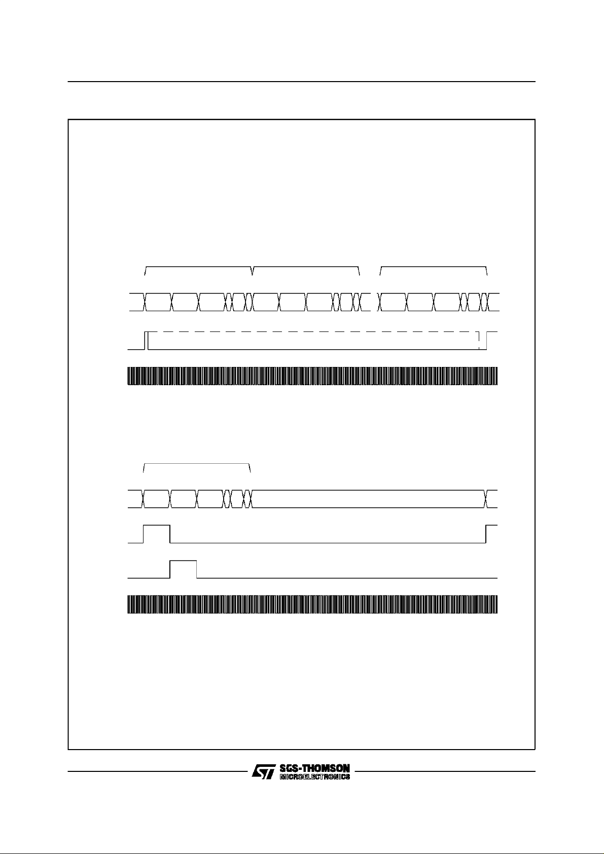
Figure4b: GCI interface format.
STLC5411
Figure 4b:
Bx/Br
FSa
BCLK
Bx/Br
GCI interface format
GCI CHANNEL 0 GCI CHANNEL 1 GCI CHANNEL 7
B1 B2 M D C/I A E
88 8242
8 KHz
GCI CHANNEL 0
B1 B2 M D C/I A E
8 8 8 242
B1 B2 M D C/I A E
8 8 8 242
SLAVE MODE
FREE
B1 B2 M D C/I A E
88 8242
FSa
FSb
BCLK
8 KHz
MASTER MODE (BCLK = 1.536MHz)
MASTERMODE
19/72

STLC5411
Figure4c: GCI multiplex examples, (slave mode).
20/72
STLC5411
Data is transmitted in both directions at half the
data clock rate. The information is clocked by the
transmitteron the front edge of the data clock and
can be accepted by the receiver after 1 to 1.5 period of the data clock.
The data clock (BCLK) is a square wave signal at
twice the data transmission frequency on Bx and
Br with a 1 to 1 duty cycle. The frequency can be
choosen from 512 to 6176 kHz with 16 kHz
modularity. Data transmission rate depends only
on the data clock rate.
The Frame Clock FSa is a 8 kHz signal for synchronization of data transmission.The front edge
of this signal gives the time reference of the first
bit in the first GCI input and output channel, and
reset the slot counter at thestart of each frame
When some GCI channels are not selected on
devices connected to the same GCI link, these
time slots are free for alternativeuses.
GCI configuration selection is done by biasing of
input pins MW, M0, CONF1, CONF2 accordingto
TABLE1.
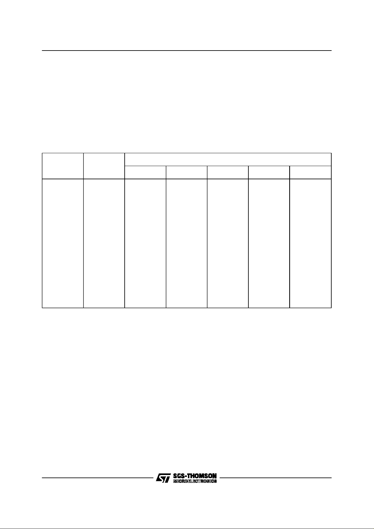
Table 1: GCI Configurationselection.
Pin Number Pin name
LT/NT12* NT/TE NT1-AUTO LT-RR-AUTO NT-RR-AUTO
28MW00000
27 M0 0 1 1 1 1
19 S1/CONF1 S1 0 1 1 0
17 S2/CONF2 S2 1 1 0 0
7 S0/FSb/TEST2 S0 FSb TEST2 TEST2 TEST2
Configuration
18 IO1/ES1 IO1 IO1 ES1 PLDD ES1
16 IO2/ES2 IO2 IO2 ES2 EC ES2
15 IO3/EC IO3 IO3 EC LFS LFS
14 IO4/TEST1 IO4 IO4 TEST1 TEST1 TEST1
22 SFSx/RFS SFSx SFSx SFSx RFS RFS
* DifferentationbetweenLT and NTconfigurationdone by bit NTS inCR2 register; GCI in slavemode.
When NT1-AUTO or NT-RR-AUTO configuration is selected, BCLK bit clock frequency of 512 kHz is
automaticallyselected
WhenNT configurationis selected,BCLK bit clockfrequency of 1536 kHz is automaticallyselected.
* *Connected to V
throughinternal pull-up resistors.
CC
21/72
STLC5411
Monitorchannel
The Monitor channel is used to write and read all
STLC5411 internal registers. Protocol on the
Monitor channel allows a bidirectional transfer of
bytes between UID and a control unit with acknowledgementat each received byte. Bytes are
transmitted on the Br output and received on the
Bx input in the Monitor channel time slot.
A write or read cycle is always constituted of two
bytes.(seefig. 5). It is possible to operate several
write or read cycles within a single monitor message.
Note: Special format is used for EOC channel.
Writecycle
The format to write a message into the UID is:
A7 A6 A5 A4 A3 A2 A1 A0
1st byte
D7 D6 D5 D4 D3 D2 D1 D0
2nd byte
A7-A1:
A0:
D7-D0:
Register Address
Write/Readback Indicator
Register Content
After the first byte is shifted in, Register address
is decoded. A0 set low indicatesa write cycle: the
content of the following received byte has to be
loadedinto the addressed register.
A0 set high indicates a read-back cycle request.
the second byte content is not significative.
STLC5411 will respond to the request by sending
back a message with the register content associated with its own address. It is then possible for
the microprocessor to receive the required register content afterseveral other pending messages.
To avoid any loss of data, it is recommended to
operateonly one read-backrequest at a time.
Note: Special format is used for EOC channel.
Readcycle
When UID has a register content to send to the
controller, it send it on the monitor channel directly. Note that the data to send can be the content of a Register previously requested by the
controllerby meansof a read-back request.
The format of the message sent by the UID is:
A7 A6 A5 A4 A3 A2 A1 A0
1st byte
D7 D6 D5 D4 D3 D2 D1 D0
2nd byte
A7-A1:
A0:
Register Address
forced to 0is spontaneous
interrupt, forced to 1 if readback
D7-D0:
Register Content
Exchange Protocol
STLC5411 validates a received byte if it is detected two consecutive times identical. (see fig. 5)
The exchangeprotocol is identical for both directions. The sender uses the E bit to indicate that it
is sending a Monitor byte while the receiver uses
A bit to acknowledge the received byte.When no
message is transferred, E bit and A bit are forced
to inactive state.
A transmission is started by the sender (Transmit
section of the Monitor channel protocol handler)
by putting the E bit from inactive to active state
and by sending the first byte on Monitor channel
in the same frame. Transmission of a message is
allowed only if A bit sent from the receiver has
been set inactive for at least two consecutive
frames. When the receiver is ready, it validates
the incoming byte when received identical in two
consecutive frames. Then, the receiver set A bit
from the inactive to the active state (preacknowledgement) and maintain active at least in the following frame (acknowledgement).
If validation is not possible (two last bytes received are not identical) the receiver aborts the
message by setting the A bit active for only a single frame.The second byte can be transmitted by
the sender putting the E bit from the active to the
inactivestate and sending the secondbyte on the
Monitor channel in the same frame . The E bit is
set inactive for only one frame. If it remains inactive more than one frame, it is an end of message. The second byte may be transmitted only
after receiving of the pre-acknowledgementof the
previous byte . Each byte has to be transmittedat
least in two consecutiveframes.
The receiver validates the current received byte
as for the first one and then set the A bit in the
next two frames first from the active state to the
inactivestate (pre-acknowledgement)and back to
the active (acknowledgement).If thereceiver cannot validates the received current byte (two bytes
received not identical)it pre-acknowledges normally but let the A bit in the inactive state in the
next frame which indicates an abort request . If a
message sent by the UID is aborted, the UID will
send again the complete message until receiving
of an acknowledgement . A message received by
the UID can be acknowledged or aborted with
flow Control.
The most significant bit (MSB) of Monitor byte is
sent first on the Monitor channel. E & A bits are
active low and inactive state on Br is 5 V. When
no byte is transmitted, Monitor channel time slot
22/72
 Loading...