

FOUR CHANNEL CODEC AND FILTER
■
FULLY PROGRAMMABL E MONOLITHIC 4
CHANNEL CODEC/FILTER
■
SINGLE +3.3 V SUPPL Y
■
A/m LAW PROGRAMMABLE
■
LINEAR CODING (16 BITS) OPTION
■
PCM HIGHWAY FORMAT AUTOMATICALLY
DETECTED:1.536 or 1.544 MHz2.048, 4.096,
8192 MHz
■
TWO PCM PORTS AVAILABLE
■
TX GAIN PROGRAMMING: 33dB RANGE;
<0.01dB STEP
■
RX GAIN PROGRAMMING:42dB RANGE;
<0.01dB STEP
■
PROGRAMMABLE SLIC INPUT IMPEDANCE
■
PROGRAMMAB LE TRANSHYBRI D BALANCE
FILTER
■
PROGRAMMABLE EQUALIZATION
(FREQUENCY RESPONSE)
■
PROGRAMMABLE TIME SLOT ASSIGNMENT
■
DIGITAL AND ANALOG LOOPBACKS
■
SLIC CONTROL PORTSTATIC (16 I/Os)
DYNAMIC (12 I/Os + 4 CS)
■
BUILT-IN TEST MODE WITH TONE
GENERATION , MC U ACC ESS TO PCM DATA
■
64 TQFP (10X10mm) PACKAGE
■
PROGRAMMABLE SLIC LINE CURRENT
LIMITATION
■
PROGRAM M A BL E S LIC OF F- HOOK
DETECTION THRESHOLD
DESCRIPTION
The STLC5048 is a monolithic fully programmable 4
channel CODEC and filter. It operates with a single
+3.3V supply.
The analog interface is based on a receive output
STLC5048
FULLY PROGR AMM A B LE
TQFP64 (10x10mm)
ORDERING NUM BER: STLC 5048
buffer driving the SLIC RX input and on an amplifier
input stage normally driven by the SLIC TX output.
Due to the single supply voltage a midsupply reference level is generated internally by the device and
all analog signals are referred to this level (AGND).
The PCM interface uses one common 8KHz frame
sync. pulse for transmi t and r eceive dir ection. The bit
clock is automatically detected between four standards: 1.563/1.544MHz, 2.048MHz, 4.096MHz,
8192MHz.
Two PCM port are provided: the channels can be
connected to port A or/and B.
Device programmability is achieved by means of
several registers and commands allowing to set the
different parameters like TX/RX gains, line impedance, transhybrid balance, equalization (frequency
response), encoding law (A/
independent channels power up/down, loopbacks,
PCM bits offset.
The STLC5048 can be programmed via serial interface running up to 8 MHz. One interrupt output pin is
also provided.
A GUI interface is also available to emulate and program the coefficients for impedance synthesis, echo
cancelling and channel filtering.
µ
), time slot assignment,
January 2003
1/45

STLC5048
BLOCK DIAGRAM
ANALOG FRONT END
VFRO0
VFX10
VFRO1
VFX11
VFRO2
VFX12
VFRO3
VFX13
VCC VEE
D/A
CH0
GR0
A/D
CH0
GX0
D/A
CH1
GR1
A/D
CH1
GX1
D/A
CH2
GR2
A/D
CH2
GX2
D/A
CH3
GR3
A/D
CH3
GX3
VDD VSS SUB CAP M1 M0
DIGITAL PROCESSOR
16
16
A/U LAW
ENCODER
8
PLL
BLOCK
8
BIAS
GENER.
SLIC
THR
A/U LAW
DECODER
INTERPOLAT.
DECIMATORS
KD FILTERS
to analog FE
DATA INTERFACE
SHAPPIRE
MACRO
CONTROLLER
CONFIG.
REGISTERS
INTERFACE
CONTROL INTERFACE
SERIAL
INTERFACE
FS
PCM
COEFF BUS
SLIC
INTERFACE
MCLK
DRA
DRB
DXA
DXB
TSXA
TSXB
IO11
IO10
IO9
IO8
IO7
IO6
IO5
IO4
IO3
IO2
IO1
IO0
CS3
CS2
CS1
CS0
INT
CCLK
CI
CO
CS
ITH ILIM VBG
D00TL467
ABSOLUTE MAXIMUM RATINGS
Symbol Parameter Value Unit
V
CC
V
DD
VD
VAin Analog Input Pin Voltage(
T
STG
T
LEAD
VCC to V
VDD to V
Digital Input Pin Voltage 5.5 V
IN
EE
SS
V
DD=VCC
; VEE=V
)V
SUB
4.6 V
4.6 V
+ 0.5;
CC
V
EE
Storage Temperature Range -65 to +150 °C
Lead Temperature (soldering, 10s) 300 °C
- 0.5 V
OPERATING RANGE
Symbol Parameter Value Unit
V
CC
, V
T
OP
Supply Voltage 3.3 +/- 5% V
DD
Operating Temperature Range -40 to +85 °C
THERMAL DATA
Symbol Parameter Value Unit
2/45
R
th j-amb
Thermal Resistance Junction-Ambient 70 °C/W
STLC5048
y
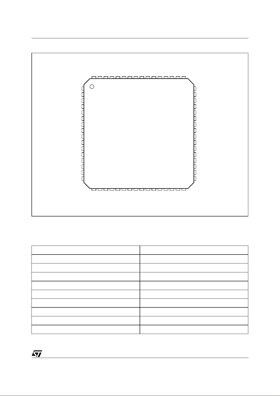
PIN CONNECTION
(Top view)
1
N.C.
2
N.C.
3
INT
4
CS
5
CO
6
CI
VSS
VDD
DRA
DXA
FS
DXB
DRB
7
8
9
10
12
13
14
15
16
CCLK
TSXA
MCLK
IO7
IO6
N.C.
RES.
60
61
62
63
64
17 18 19 20 21
IO9
IO10
IO11
IO8
59 58 57 56 5455 53 52 51 50 49
22 23 24 25 26
VCC4M1VEE4
CS2_
CS3_
VEE2
271128 29 30 31 32
VEE3
VBG
48
47
46
45
44
43
42
41
40
39
38
37
36
35
34
33
VFRO3
ILIM
VFXI3
VCC3
VCC2
VFXI2
VFRO2
SUB
CAP
VFRO1
VFXI1
VCC1
VCC0
VFXI0
ITH
VFRO0
PIN DESCRIPTION
I/O DEFINITION
N.C.
TSXB_
IO0
IO1
IO2
IO3
IO4
IO5
VCC5
VEE5
M0
CS0_
CS1_
VEE1
VEE0
RES
D94TL150
Type Definition
AI Analog Input
AO Analog Output
ODO Open Drain Output
DI Digital Input
DO Digital Output
DIO Digital Input / Output
DTO Digital Tristate Output
DPS Digital Power Supply
APS Analog Power
Suppl
3/45
STLC5048
PIN DESCRIPTION
(continued)
ANALOG PIN DESCRIPTION
No. Name Type Description
33 VFRO0 AO Receive analog amplifier output channel 0. PCM data received on
the programmed Time Slot on DR input is decoded and appears at
this output.
39 VFRO1 AO Receive analog amplifier output channel 1. PCM data received on
the programmed Time Slot on DR input is decoded and appears at
this output.
42 VFRO2 AO Receive analog amplifier output channel 2. PCM data received on
the programmed Time Slot on DR input is decoded and appears at
this output.
48 VFRO3 AO Receive analog amplifier output channel 3. PCM data received on
the programmed Time Slot on DR input is decoded and appears at
this output.
35 VFXI0 AI TX Input Amplifier channel 0. Typ 1MΩ input impedance
38 VFXI1 AI TX Input Amplifier channel 1. Typ 1MΩ input impedance
43 VFXI2 AI TX Input Amplifier channel 2. Typ 1MΩ input impedance
46 VFXI3 AI TX Input Amplifier channel 3. Typ 1MΩ input impedance
40 CAP AGND Voltage filter pin: a 100nF capacitor must be connected
between ground and this pin.
34 ITH AO SLIC Off Hook detection threshold.
47 ILIM AO SLIC line current limitation.
49 VBG AI SLIC VBG reference for DC characterisrics programmability.
NOT CONNECTED
2, 18, 63, 1 N.C. Not Connected, must be left open
32, 64 RES Reserved pins, must be connected to ground
POWER SUPPLY PIN DESCRIPTION
25,36,
37,44,
45,56
26,30,
31,50,
51,55
9 VDD DPS Digital Power supply 3.3V, require 100nF decoupling capacitor to
8 VSS DPS Digital Ground.
41 SUB DPS Substrate connection. Must be shorted together with VEE and VSS
VCC0..5 APS Total 6 pins: 3.3V analog power supplies, should be shorted together,
require 100nF decoupling capacitor to VEE.
VEE0..5 APS Total 6 pins: analog ground, should be shorted together.
VSS.
pins.
4/45
STLC5048
PIN DESCRIPTION
(continued)
DIGITAL PIN DESC RIPTION
No. Name Type Description
27
54
14 FS DI Frame Sync. Pulse. A pulse or a square waveform with an 8kHz
13 MCLK DI Master Clock Input.
12 TSXA ODO Transmit Time Slot (open drain output, 3.2mA). Normally it is floating
M0
M1
DI Mode Select.
M1 M0 Mode select
0 0 Reset Status
1 0 Normal Operation
0 1 Not Allowed
1 1 Not Allowed
repetition rate is applied to this pin to define the start of the receive
and transmit frame. Effective start of the frame can be then shifted of
up to 7 clock pulses independently in receive and transmit directions
by proper programming of the PCMSH register.
Four possible frequencies can be used:
1.536/1.544 MHz; 2.048 MHz; 4.096 MHz; 8.192 MHz.
The device automatically detect the frequency applied.
This signal is also used as bit clock and it is used to shift data into
and out of the DRA/B and DXA/B pins.
in high impedance state except when a time slot is active on the DXA
output. In this case TSXA output pulls low to enable the backplane
line driver.
11 DXA DTO Transmit PCM interface A. It remains in high impedance state except
during the assigned time slots during which the PCM data byte is
shifted out on the rising edge of MCLK.
10 DRA DI Receive PCM interface A. It remains inactive except during the
assigned receive time slots during which the PCM data byte is shifted
in on the falling edge of MCLK.
24 IO5 DIO General control I/O pin #5. Can be programmed as input or output via
DIR register. Depending on content of CONF register can be a static
input/output or a dynamic input/output synchronised with the CSn
output signals controlling the SLICs.
62 IO6 DIO General control I/O pin #6. (see IO5 description).
61 IO7 DIO General control I/O pin #7. (see IO5 description).
60 IO8 DIO General control I/O pin #8. (see IO5 description).
59 IO9 DIO General control I/O pin #9. (see IO5 description).
58 IO10 DIO General control I/O pin #10. (see IO5 description).
57 IO11 DIO General control I/O pin #11. (see IO5 description).
19 IO0 DIO General control I/O pin #0. (see IO5 description).
20 IO1 DIO General control I/O pin #1. (see IO5 description).
21 IO2 DIO General control I/O pin #2. (see IO5 description).
22 IO3 DIO General control I/O pin #3. (see IO5 description).
23 IO4 DIO General control I/O pin #4. (see IO5 description).
5/45
STLC5048
PIN DESCRIPTION
(continued)
DIGITAL PIN DESCRIPTION (continued
No. Name Type Description
28 CS0 DIO Slic CS control #0. Depending on CONF reg. content can be a CS
29 CS1 DIO Slic CS control #1, (see CS0 description).
53 CS2 DIO Slic CS control #2, (see CS0 description).
52 CS3 DIO Slic CS control #3, (see CS0 description).
4 CS DI Chip Select Input, when this pin is low control information can be
7 CCLK DI Clock of Serial Control Bus. This clock shifts serial control information
6 CI DI Control Data Input of Serial Control Bus.
output for SLIC #0 or a static I/O.
When configured as CS output it is automatically generated by the
CODEC with a repetition time of 31.25ms. In this mode also the
IO0..11 are synchronised and carry proper data in and out
synchronous with CS.
When configured as static I/O, the direction is defined by CSDIR
register content.
written to or read from the device via the CI and CO pins.
into or out of CI or CO when CS input is low depending on the current
instruction. CCLK may be asynchronous with the other system
clocks.
Control data is shifted in the device when CS is low and clocked by
CCLK. Depending on the addressed register different numbers of
consecutive bytes can be loaded.
5 CO DI Control Data Output of Serial Control Bus.
Control data is shifted out the device when CS is low and clocked by
CCLK. Depending on the addressed register different numbers of
consecutive bytes can be shifted out.
3 INT ODO Interrupt output (open drain), goes low when a data change has been
detected in the I/O pins or another interrupt source is active. One
mask register allows to mask any I/O pin. Interrupt is reset when the I/
O register is read.
17 TSXB ODO Transmit Time Slot (open drain output, 3.2mA). Normally it is floating
in high impedance state except when a time slot is active on the DXB
output. In this case TSXB output pulls low to enable the backplane
line driver.
15 DXB DTO Transmit PCM interface B. It remains in high impedance state except
during the assigned time slots during which the PCM data byte is
shifted out on the rising edge of MCLK.
16 DRB DI Receive PCM interface B. It remains inactive except during the
assigned receive time slots during which the PCM data byte is shifted
in on the falling edge of MCLK.
6/45
STLC5048
FUNCTIONAL DESCRIPTION
The STLC5048 i s a fully p rogrammabl e device wi th embedd ed ROM and RAM. The ROM is used to contain t he defau lt
state coefficients for the pro gramm able filters, whi le t he RAM is used to load the desired coeffi cient values.
POWER ON INITIALIZATION
When power is first applied it is recommended to reset the device (M1=M0=0) in order to set all the internal reg-
isters to the reset value (see register description); this means also power down mode for all the four channels
and SW reset bit (RES) set in the CONF register.
When the RES bit is set, the only instructi ons allowed are the one that dis able this bit and the REACOM instruction: all other instructions are ignored. It is not possible to disable the RES bit and write the other bits of the
CONF register with the same instruction.
Of course, RESET mode can be programmed also by writing the RES bit of the CONF register.
See appendix C for the power up sequence.
During RESET condition all the I/On and CSn pins are set as inputs, DX is in high impedance and all VFROn
are set to AGND. After the reset all registers are loaded with the reset value.
It means that the PCM interface and all the VFRO outputs ar e configured as descri bed in the Power Down State,
while no transmit or receive time slot are set.
Then, filters and gain blocks are configured with the coefficient defined in the Default State.
POWER DOWN STATE
Each of the four channel may be put into power down mode by setting the appropriate bit in the CONF register .
In this mode the eventual programmed D X channel i s s et in high im pedance while the VFRO outputs are forced
to AGND. When all the channels are set in Power Down mode the device enters the Power Down state: all the
blocks related to the data processing are turned off, while the RAM is On or Off according to the PDR bit value
in the COMEN register.
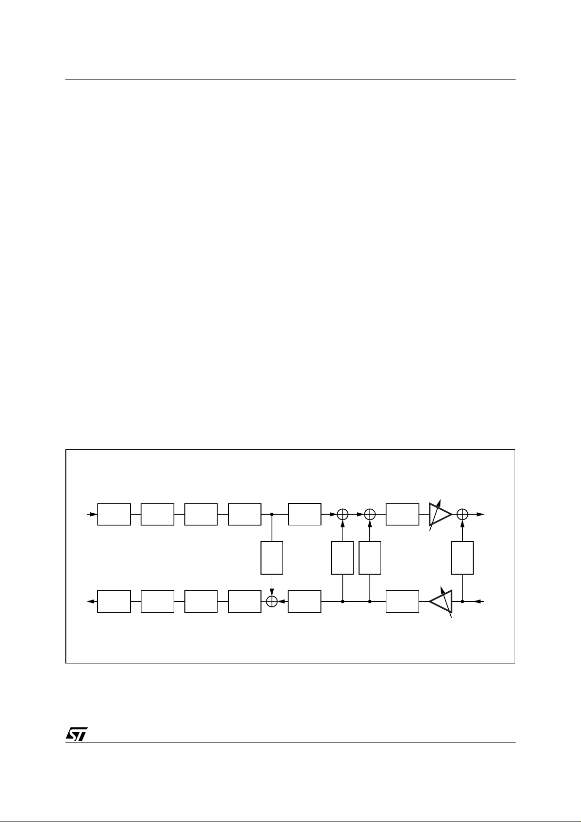
Figure 1. Block Diagram of a single channel.
** *
A/muDR VFRO
A/muDX HPX X GX
* PROGRAMMABLE BLOCKS
HPR R GR
**
RX
LPR D/A
*** *
B Z KD KA
*
LPX
A/D
TX
VFXI
D00TL468
7/45
STLC5048
FUNCTIONAL DESCRIPTION (continued)
RINGING STATE
This state can be used during the ringing phase in order to transmit a low frequency ringing signal (25-50 Hz).
In order to obtain a 1 Vrms ringing signal at VFRO output a digital signal DR equal to -0.78dBm0 must be provided.
This state means B, Z, X, K D and KA bloc ks equal to open c ircuits and the R bloc k configured in order to obtain
the maximum gain at the frequency of 25-50 Hz. During the ringing state if the TX time slot is enabled the idle
PCM code is forced to DX.
To switch to this state, a bit (FR0..3) in the COEFST register must be set for every channel.
The programmed values for the previous blocks become active only when the FR and FD bits are reset.
If both FR and FD bits of a channel are set, the selected coefficient will be those of the Ringing State.
IMPEDANCE SYNTHESYS
The impedance synthesis is performed by fully digital filters (Z and KD) and by an analog path (KA).
The Z, KD and KA filters report to the receive path the feedback signal coming from the transmit path. The co-
efficients of the Z, KD and KA filters are programmed via the ZFC, KD and AFE_CFF commands respectively.
ECHO CA NCELING
The trans-hybrid balance is performed by the digital programmable filter B.
The B filter reports to the transmit path the signal coming from the receive path. The coefficient of the B filter
are programmed via the BFC command.
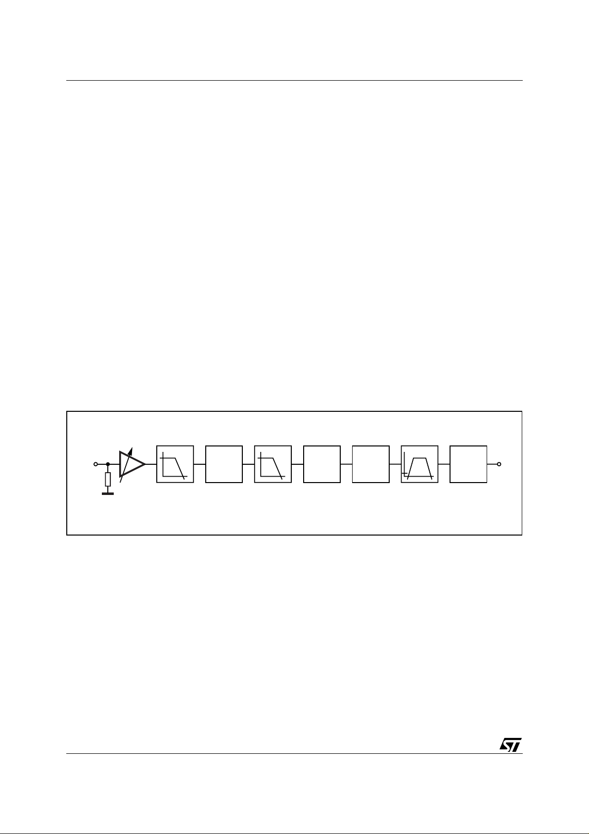
Figure 2. Trans m i t pat h.
TXG
VFXI
1MΩ
AGND
Σ∆
CONV.
for TXG=0dB; GX=0dB (FF)
61mVms => 0dBm0
GXO A/µGX
D00TL469
DX
TRANSMIT PATH
The transmit section input consist of the input amplifier, the A/D converter, the equalization filter X, the gain
block GX, the encoder and the channel filters (LPX and HPX).
The input amplifier is provided of a programmable gain with a typical input impedance of 1M
Ω
. The amplifier
gain can be programmed with two different values (0dB, +3.52dB) by means of the TXG Register.
VFXI input must be AC coupled to the signal; the voltage swing allow ed is 1.4Vpp when the pre amplifier gai n is
set to 0dB and 0.93Vpp when the gain is 3.52dB; higher levels must be reduced through proper dividers.
Following the input amplifier the signal is converted into digital domain and a X filter block is programmed to
equalise together with the HPX and LPX filters the frequency response. The coefficients of the X filter are programmed via the XFC command.
A gain block (GX) allows to set the transmit level in a 30dB range, with steps <0.01dB. This block can be programmed via the GTX command.
8/45
STLC5048
FUNCTIONAL DESCRIPTION (continued)
The needed TX gain can be set by proper programming of the GX block in combination with the TX amplifier.
Setting GTX=00h, the transmitted signal is muted and an idle PCM signal is generated on DX.
Concerning the CODING function, A/m law can be selected writing the CONF register (bit 5 AMU). In addition,
via the CONF register (bit 6 LIN) the coding law can be set to linear mode (16 bits). In this case the signal sent
on the DX will take two adjacent PCM channels, proper care has to be take n in the time slot sel ection pr ogramming (DXTS register).
The intrinsec non programmable gain GX0 set the TX path gain to 22.07dB. The absolute gain level (see electrical characteristics) refers to this intrinsec gain.
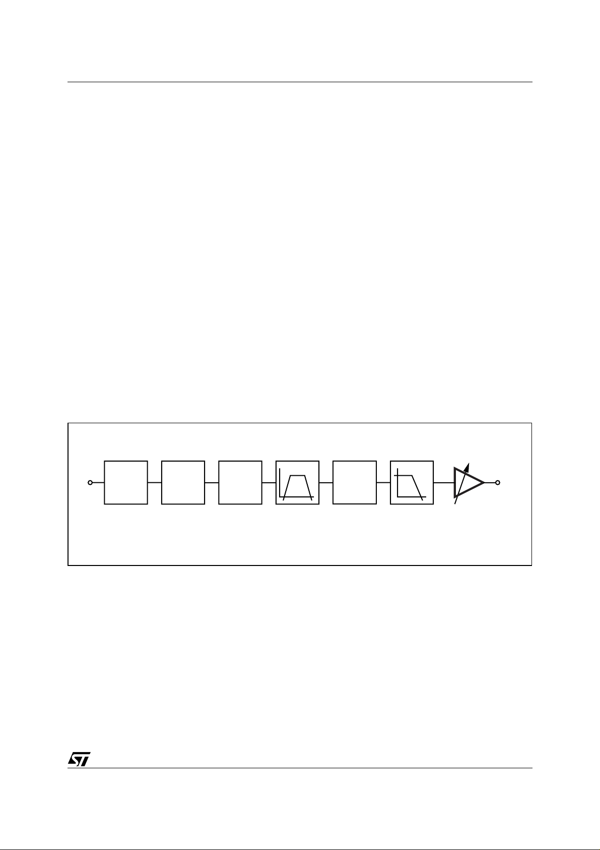
RECEIVE PATH
The receive path of the STLC5048 consists of the decoder section, the gain block GR, the R filter, the channel
filters (LPR, HPR) the D/A converter and the output amplifier.
Concerning the DECODING function, A/m law can be selected writing the CONF register (bit 5 AMU). In addition
via the CONF register (bit 6 LIN) the coding law can be set to linear mode (16 bits).
In this case the signal received on the DR input will take two adjacent PCM channels, proper care has to be
taken in the time slot selection programming (DRTS register).
The gain block GR is controlled by the GRX command allowing 30dB gain range in 0.01dB steps.
The R filter together the channel filters (LPR and HPR) performs the line equalization. The coefficients of the R
filter are programmed via the RFC command.
The signal is converted in the analog domain and amplified by the RX amplifier that can be programmed with
four different values (mute, 0dB, -6dB and -12dB) by means of RXG register.
Figure 3. Receive path.
RXG
DR
GROA/µ GR
D00TL470
Σ∆
CONV.
for RXG=0dB; GR=0dB
0dBm0 => -3dBm/
600Ω
VFRO
VFRO output, referred to AGND must be AC coupled to the load, r eferred to V SS, to prevent a DC cur rent flow.
In order to get the best noise performances it is recommended to keep GRX value as close as possible to the
maximum (FFh) setting properly the additional attenuation by means of RXG.
The intrinsec non programmable gain GR0 set the RX path gain to -3.15dB. The absolute gain level (see elec-
trical characteristics) refers to this intrinsec gain.
PCM INTERFAC E
The STLC5048 dedicates eight pins to the interface with the PCM highways.
MCLK represents the bit clock and is also used by the device as a source for the clock of the internal PLL.
Five possible frequencies can be used: 1.536/1.544MHz (24 channels PCM frame); 2048MHz (32 channels
PCM frame); 4.096MHz (64 channels PCM frame); 8.192MHz (128 channels PCM frame). The operating fre-
9/45
STLC5048
quency is automatical ly detected by the device the fi rst time both MCLK and FS are applied and becomes acti ve
after the second FS period. MCLK synchronises both the transmit data (DXA/B) and the receive data (DRA/B).
The Frame Sync. signal FS is the common time base for all the four channels.
Transmit and Receive programmable Time-Slots are framed by an internal sync. signal that can be coincident
with FS or delayed of 1 or 7 MCLK cycles depending on the programming of PCMSH register.
Two PCM ports are available: every channel can be connected to a different PCM port by means of PCMCOM
register.
DXA/B represents the transmit PCM interface. It remains in high impedance state except during the assigned
time slots during which the PCM data byte is shifted out on the rising/falling edge of MCLK according to the TE
bit of PCMCOM register. The four channels can be shifted out in any possible timeslot as defined by the DXTS
registers. The assigned Time Slot (Transmit and Receiv e) takes pl ace in the 8 MCLK cy cles follow ing the ris ing
edge of FS.
The data can be shifted out on port A and/or B according to PCMCOM register.
If one CODEC is set i n P ower Down by software programming the cor respondin g time slot is s et in High Imped-
ance. When linear coding mode is selected by CONF register programming the output channel will need two
consecutive time slots (see register description).
DRA/B represents the receive PCM interface. It remains inactive except during the assigned time slots during
which the PCM data byte is shifted in on the falling edge of MCLK. The four channels are shifted in any possible
time slot as defined by the DRTS registers.
If one Codec is set in Power Down by software programming the corresponding time slot is not loaded and the
VFRO output is kept at steady AGND level.
INSTRUCTION B YTE STRUCTURE
First Byte (Address or command ID) Following Bytes (Data)
7654321076543210
R/WI6 I5 I4 I3 I2 I1 I0 D7D6D5D4D3D2D1D0
R/W= 0: Write Opera tion
R/W
=1: Read Operation
I6..I0: In st ruction Ide ntifier: it ca n be a register address or a command identifier.
The numbe r of data bytes depends on the in st ruction ty pe. T he first bit of a byte is the MSB, the first byt e of an instruction is the LSB yte.
When linear coding mode is selected by CONF register programming the input channel will need two consecutive time slots (see register description).
The data can be shifted in from port A or B according to the PCMCOM register.
TSXA/B represents the Transmit Time Slot (open drain output, 3.2mA). Normally it is floating in high impedance
state except when a time slot is active on the DXA/B output. In this case TSXA/B output pulls low to enable the
backplane line driver. Should be strapped to VSS when not used.
Finally by means of the LOOPB register it is possible to implement a digital or analog loopback on any of the
selected channels.
MCU CONTROL I NTERFACE
The MCU serial control interface consists of 4 pins.
CCLK: Control Clock
CI: Serial Data In
CO: Serial Data Out
CS: Chip Select Input
Control instructions require at least two bytes: however two single byte instructions are also provided.
10/45

STLC5048
In the multiple byte instructions the fir st one specifies the command or the register address and the acces s type
(Read or Write).
The following bytes c ontain the data t o be loaded int o the i nternal RAM (on C I wire) or c arry out the RAM content
(on CO wire) depending on the R/W bit of t he fir st byte. CO wire is nor mally in High Impedance and goes to low
impedance only after the first byte i n case of Read operation. This al lows to us e a c ommon wir e for both CI/CO.
CS, normally High, is set Low during the tr ans missi on/reception of a byte, l asting 8 CCLK pulses. Between two
consecutive access the CS must be set high.
The CCLK can be a continuos or a gated clock.
The result of any instru ction (read/writ e oper ation), if negativ e, can generate an interrupt (maskable). The interrupt register (INT) contains the cause information of the generated interrupt and it is cleared every time that it
is read.
Depending on the instruction specified in the first byte, the STLC5048 waits a defined number of data bytes. If
the STLC5048 doesn't receive the data byte within a predefined period specified by means of T_OUT command,
an internal time out rejects the instruction. The time-out time is verified between two consecutive MCU interface
access (between the falling edge of the CS and the following rising edge).
This feature is us ed to verify the sy nchr onisati on of the MCU i nterf ace: however i t can be dis abled i f not de sir ed
(see T_OUT reg description). To check this synchronisati on is provided a specific register (SYNCK) that returns
always a predefined value: if the returned value is different the MCU interf ace is in out of sync state (the device
is waiting a data byte while the MCU is writing an address or vice versa). In this case, it is possible to realign it
by means of the execution of a specif ic singl e byte instr uc tion (REACOM) fr om 1 to 53 times, depending on the
instructions .
Every time an illegal operation (access to not allowed address, time-out violation or clock pulse dif ferent than 8
inside a CS active) is performed the MCU interface is put on an error state: to resume it from this state a single
REACOM instruction can be used.
Anyway after a REACOM instruction a successful SYNC instruction guarantees the correct synchronisation.
One additional wire provided to the control interface is an open drain interrupt output (INT) that goes low when
a change of status is detected on the I/O pins or other interrupt source are active (see INT register). INT is automatically reset aft er reading of the register co rresp onding the c ause that has generated the inter rupt (see INT
register description).
A particular register (COMEN) allows to enable a command on different channel at the same time. Every time
a command operation is performed at least one channel must be enabled in this register.
This feature is useful when all channels must be configured in the same condition. When a command is used
to perform a read operation only one channel can be enabled at the same time.
To check the confi guration of the devi ce a check sum value is provided. This v alue is cal culated on all coefficient
parameters entered (coefficients of KD, AFE_CFF, GRX, GTX, RFC, XFC, BFC, ZFC blocks; see CKSUM register description). Two commands are required to get this value: the first one (CKSTART) starts the internal
checksum calculation, the second one (CKSUM) returns the calculated value. Between this two commands no
other operation are allowed. The checksum value is available within 400us the CKSTART command.
Coefficient checksum is defined by this algorithm:
This algorithm guarantees a fault coverage of 1 - 2
16
X
+ X12 + X5 + 1
-16
.
PROGRAMMING T HE DEVICE
After the power up, the filters and gain blocks can be pro grammed also with all the channels set in Power Down.
In this case the PDR bit of the COMEN register must be set to 0.
With the proper setting of the COMEN register, the commands can be applied to more than one channel at the
same time.
To read the coefficient values loaded in the RAM, only one channel per time must be enabled in the COMEN
register.
11/45
STLC5048
SLIC CONTROL INTERFACE
The device provides 12 I/O pins plus 4 CS signals. The interface can work in dynamic or static mode: it can be
selected by means of STA bit of the CONF register.
■
Dynamic Mode: the I/O pins are configured as input or output by means of DIR register. The CS signals
are used to select the different SLIC interface. In this case the I/O pin can be multiplexed. The data
loaded from SLIC #n via I/O pins configured as input can be read in the DATAn register. The data written
in a DATAn register will be loaded on the I/O pins configured as output wh en the Csn signal will be
active.
■
Static Mode: The CS signal can be us ed a s I/O pins. They can be configured as input or output I/O by
means of DATA1 register. The data corresponding to the CS signal can be read or written by means of
DATA2 register. All data related to the other I/O pins can be read or written by means of DATA0 register.
DC SLIC PROGRAMMA BILITY
Three additional pins are used to select the On-Hook/Off-Hook detection threshold and the line card limitation
of the STLC3080 SLIC. This two values are programmed by ILIM and ITH registers. The programmation of
these two registers must be done before the filter coefficients download.
The VBG input pin must be connected to the IREF pin of the STLC3080.
When the L3235N is used in kit with STLC5048 the ILIM, ITH and VBG pin must be not connected.
BUILT IN TEST
By means of TONEG register it is possible to inject a tone of var iable frequency (25Hz, 1 and 3KHz) and 0dBm0
amplitude into the receiv e path, replacing any signal coming from the PCM inter face. This test can be performed
on every channel.
Setting the proper bit of the PCMCOM register is also possible to read/write the PCM data coming from the
transmit path via the MCU interface (PCMRD/PCMWD registers). This feature can be enabled only on one
channel per time.
These two features can be used to test the line interface operation.
REGISTER ADDRESSES
Addr Nam e Description
00h DIR-L I/O Direction (bit 7-0)
01h DIR-H I/O Direction (bit 11-8)
02h DATA0-L I/O Data ch#0 (bit 7-0)
03h DATA0-H I/O Data ch #0 (bit 11-8)
04h DATA1-L I/O Data ch#1 (bit 7-0)
05h DATA1-H I/O Data ch #1 (bit 11-8)
06h DATA2-L I/O Data ch#2 (bit 7-0)
07h DATA2-H I/O Data ch #2 (bit 11-8)
08h DATA3-L I/O Data ch#3 (bit 7-0)
09h DATA3-H I/O Data ch #3 (bit 11-8)
0Ah PCHK-A Persistency Check Time for input A
0Bh PCHK-B Persistency Check Time for input B
10h INT Interrupt regist er
12/45

STLC5048
REGISTER ADDRESSES
11h DMASK-L Int. Mask I/O Port (03h)
12h DMASK-H Int. Mask I/O Port (04h)
Addr Name Description
13h IMASK Interrupt Mask reg.
14h ALARM Alarm register
20h CONF Configuration register
21h COMEN Command Enable reg.
23h SYNCCK Synchronous Check reg.
25h CTRLACK DSP status register
26h CKSUM-L Cheksum register L
27h CKSUM-H Cheksum register H
2Ah LOOPB Loopback register
2Bh TXG Transmit preamp. Gain
2Ch RXG Receive preamp. Gain
2Dh ILIM SLIC line current lim.
2Eh ITH SLIC Off-Hook threshold
50h PCMSH PCM Shift register
51h PCMCOM PCMCOM register
52h DXTS0 Transmit Timeslot ch #0
53h DXTS1 Transmit Timeslot ch #1
54h DXTS2 Transmit Timeslot ch #2
55h DXTS3 Transmit Timeslot ch #3
56h DRTS0 Receive Timeslot ch #0
57h DRTS1 Receive Timeslot ch #1
58h DRTS2 Receive Timeslot ch #2
59h DRTS3 Receive Timeslot ch #3
5Ah PCMWD -L P CMW Data regist er
5Bh PCMWD -H PCMW Data register
5Ch PCMRD-L P CMR Data regist er
5Dh PCMRD -H PCMR Data register
5Eh PCMCTRL PCM Control register
60h TONEG Tone Generation reg.
61h COEFST Coefficient State reg.
70h SWRID Software rev. ID code
71h HWRID Silicon revision ID code
(continued)
13/45
STLC5048
REGISTER DESCRIPTION
I/O Direction Register (DIR)
Addr=00h; Reset Value=00h
Addr=01h; Reset Value=X0h
BIt7 Bit6 Bit5 Bit4 Bit3 Bit2 Bit1 Bit0
R/W0000000
IO
7
IO
6
IO
5
IO
4
IO
3
IO
2
IO
1
IO
0
BIt7 Bit6 Bit5 Bit4 Bit3 Bit2 Bit1 Bit0
R/W0000001
IO
11
IO100IO
9
IO
8
IO11..0=0 I/O pin 11..0 is an input, data on the I/O input is written in DATAn register bit 11..0.
IO11..0=1 I/O pin 11..0 is an output, data contained in DATAn register bit 11..0 is transferred to the I/O output.
I/O Data Register channel #0 (DATA0)
Addr=02h; Reset Value=00h
Addr=03h; Reset Value=X0h
If bit 4 of CONF register (STA)=0 Dynamic I/O mode:
BIt7 Bit6 Bit5 Bit4 Bit3 Bit2 Bit1 Bit0
R/W0000010
D0
7
BIt7 Bit6 Bit5 Bit4 Bit3 Bit2 Bit1 Bit0
R/W0000011
D0
6
D0
5
D0
4
D0
3
D0
2
D0
1
D0
0
D0
11
D0
10
D0
9
D0
8
When CS0 is active D011..0 are transferred to the corresponding I/O pins configured as outputs (see DIR register). For the I/O pins configured as inputs the corresponding D011..0 will be written by the values applied to
those pins while CS0 is low.
If bit 4 of CONF register (STA)=1 Static I/O mode:
Bit7 Bit6 Bit5 Bit4 Bit3 Bit2 Bit1 Bit0
R/W0000010
DS
7
DS
6
DS
5
DS
4
DS
3
DS
2
DS
1
DS
0
Bit7 Bit6 Bit5 Bit4 Bit3 Bit2 Bit1 Bit0
R/W0000011
DS
11
DS
10
DS
9
DS
8
DS11..0 are transferred to the corr espondin g I/O pins configur ed as outpu ts (see DIR register ). For the I/O pins
configured as inputs the corresponding DS11..0 will be written by the values applied to those pins.
14/45
 Loading...