


®
FOR SHORT LOOP APPLICATIONS
MONOCHIP SLIC SUITABLE FOR SHORT
LOOP APPL I CATIONS
IMPLEMENTES ALL KEY FEATURES OF
THE BORSHT FUNCTION
INTEGRATED RINGIN G
SOFT BATTERY REVERSAL WITH PRO-
GRAMMABLE TRANSITION TIME
ON HOOK TRANSMISSION
LOW POWER DISSIPATION IN ALL OPER-
ATING MODES
AUTOMATIC DUAL BATTERY OPERATION
INTEGRATED RING TRIP DETECTION
METERING PULSE INJECTION
LOOP START, GROUND START FEATURES
SURFACE MOUNT PACKAGE
-40 TO +85°C OPERATING RANGE
DESCRIPTION
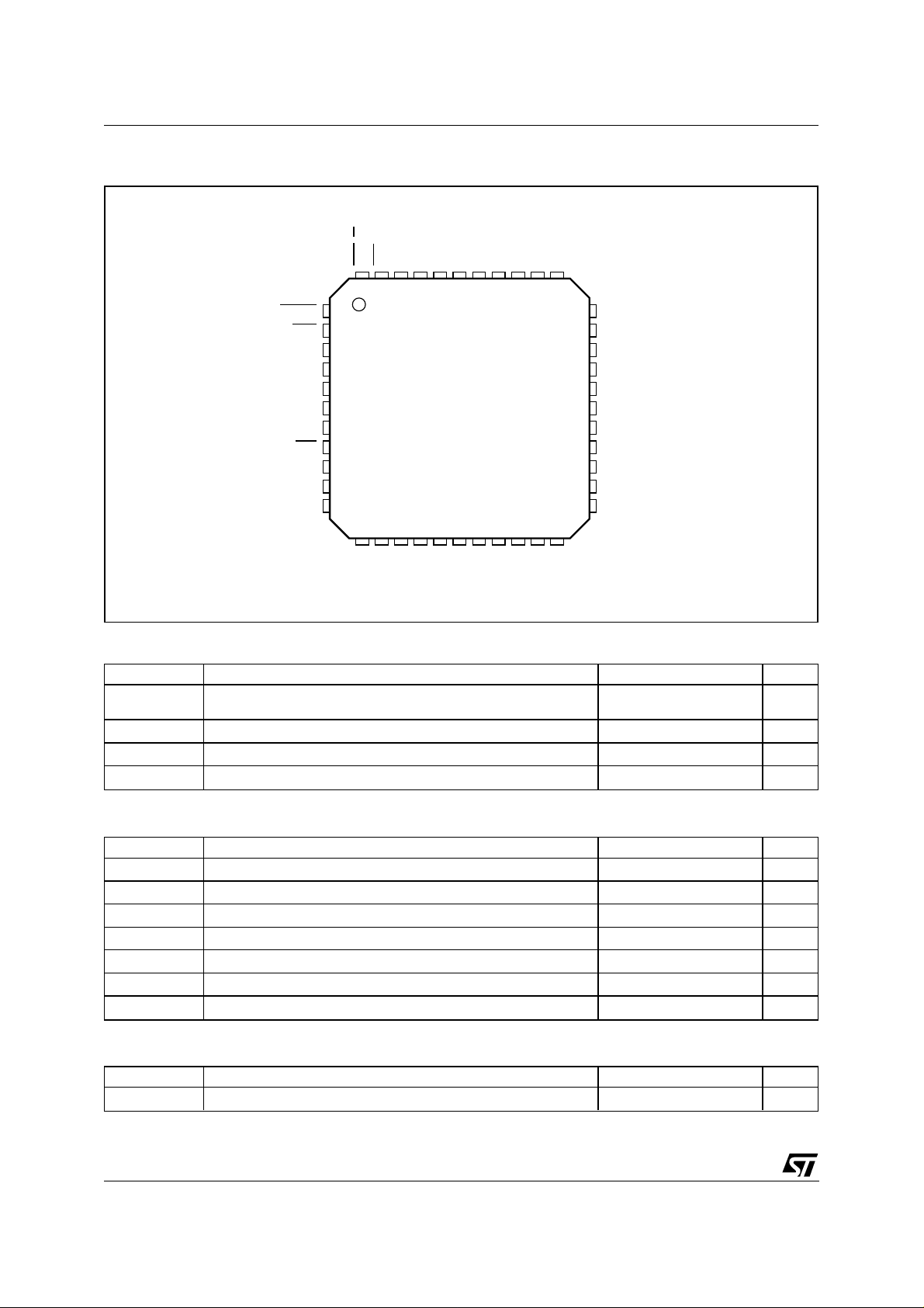
The STLC30R80 is a SLIC device suitable for
short loop applications. The SLIC provides the
STLC30R80
INTEGRATED RINGING SLIC
TQFP44 (10 x 10)
ORDERING NUMBER:
generation of the ringing signal and the standard
battery feeding with full programmability of the DC
characteristic.
In particular two external resistors allow to set the
limiting current value (up to 50mA) and the value
of the resistive feeding when not in constant current region.
STLC30R80
BLOCK DIAGRAM
DET
GDK/AL
CSIN
CSOUT
RES
SW
TTXIN
ZB
TX
RX
ZAC1
D0D1D2
LOGIC
INTERFACE
&
DECODER
AC
PROCESSOR
RSZAC
RT1 RT2CRT
LINE STATUS
ILT
SUPERVISION
COMMANDS
REFERENCE
&
BIAS SWITCHING
IREF V
CAC AGND CREV CSVR
CC
V
DD
ILL
AC+
DC
AC
DC
LINE
INTERFACE
+
DC
PROCESSOR
VBAT BASE RDC
TIP
RING
BGND
VREG
ILTF
RLIM
RTH
D99TL431AMOD
November 2001
1/13
STLC30R80
PIN CONNECTION
CSOUT
CSIN
D0
D1
D2
N.C.
N.C.
RES
VDD
VCC
CRT
BGND
RING
TIP
AGND
AGND
AGND
DET
GDK/AL
44 43 42 41 3940 38 37 36 35 34
1
2
3
4
5
6
7
8
9
10
12 13 14 15 16
SW.
N.C.
N.C.
171118 19 20 21 22
TX
ZB
VBAT
AGND
RS
VREG
ZAC
BASE
CSVR
33
32
31
30
29
28
27
26
25
24
23
RX
PINCON_STLC30R80
ZAC1
CREV
IREF
RLIM
RTH
AGND
RT1
RT2
ILTF
RDC
CAC
TTXIN
ABSOLUTE MAXIMUM RATINGS
Symbol Parameter Value Unit
V
BAT
V
CC
V
DD
Battery voltage -80 + VCC to +0.4
-80 + V
REL
to + 0.4
Positive supply voltage -0.4 to +7 V
Control Interface Supply Voltage -0.4 to +7 V
A/R/BGND AGND respect BGND -2 to +2 V
OPERATING RANGE
Symbol Parameter Value Unit
T
opT
V
CC
V
DD
V
BAT
Operating temperature range -40 to +85 °C
Positive supply voltage 4.75 to 5.25 V
Control Interface Supply Voltage 3 to 5.25 V
Battery voltage -72 to -15 V
A/BGND AGND respect BGND -0.3 to +0.3 V
PD (70) Max. power dissipation @ Tamb = 70°C 1.1 W
PD(85) Max. power dissipation @ Tamb = 85°C 0.9 W
THERMAL DATA
Symbol Parameter Value Unit
R
th j-amb
Thermal resistance Junction to Ambient Typ. 60 °C/W
V
V
2/13
STLC30R80
PIN DESCRIPTION
Pins Name Description
1
2
3 D0 Control Interface input bit 0. (*)
4 D1 Control Interface input bit 1. (*)
5 D2 Control Interface input bit 2. (*)
6 N.C. Not connected
7 N.C. Not connected
8
9V
10 V
11 CRT Ring-Trip time constant capacitor.
12 N.C. Not connected
13 N.C. Not connected
14 SW Internal switch/limiting current programming pin.
15 AGND Analog Ground
16 V
17 TX 4 wires output stage (Transmitting Port).
18 ZB Cancelling input of Balance Network for 2 to 4 wires conversion.
19 RS Protection resistors image. The image resistor is connected between this node and ZAC.
20 ZAC AC impedance synthesis.
21 ZAC1 RX buffer output/ AC impedance is connected between this node and ZAC.
22 RX 4 wires input stage (Receiving Port). A 100K external resistor must be connected to AGND to
23 TTXIN Metering Signal Input (AC) and Line Voltage Drop Programming (DC). If not used must be connectd
24 CAC AC feedback input/ AC-DC split capacitor is connected between this node and ILTF.
25 RDC DC current feedback input. The RDC resistor is connected between this node and ILTF.
26 ILTF Transversal Line Current Image.
27 RT2 Input pin to sense ringing current , for Ring-Trip detection.
28 RT1 Input pin to sense ringing current , for Ring-Trip detection.
29 AGND Analog ground.
30 RTH Off-Hook threshold programming pin.
31 RLIM Limiting current programming pin.
32 IREF Voltage reference output to generate internal reference current.
33 CREV Reverse polarity transition time programming.
34 CSVR Battery supply filter capacitor.
35 BASE Driver of the external transistor. Connected to the base.
36 VREG Regulated voltage. Provides the negative supply to the power line drivers. It is connected to the
37 BGND Battery ground.
38 RING B wire termination output. IB is the current sunk into this pin.
39 TIP A wire termination output. IA is the current sourced from this pin.
40 AGND Analog ground.
CSOUT Chip-Select for output control bits DET and GDK . Active Low. (*)
CSIN Chip-Select for input control bits latches D0 D1 D2 R0 R1 . Active Low. (*)
RES Reset Input; active low. After activation the SLIC is put in Power Down state
DD
CC
BAT
Control interface Power Supply. VDD = 3.3V or VDD = VCC.
Positive Power Supply (+5V).
Negative Battery Supply.
bias the input stage.
to AGND.
emitter of the external transistor.
3/13
STLC30R80
CONTROL INTERFACE
INPUTS
D0 D1 D2
0
0
0
0
1
1
1
0
0
1
1
0
1
1
0/1
0
1
0
1
1
0
OPERATING MODE
Power down
Stand-by
Active N.P.
Active R.P.
Ringing
High Impedance Feeding
Ground Start
A parallel interface allow to control the operation
of STLC30R80 through a control bus:
- D0 D1 D2 latched input bits defining the Slic
operation mode
DET and GDK/AL , tri-state outputs, signal the
status of the loop: On/Off-Hook and Ground-Key.
GDK/AL goes low also when the device
Pin
thermal protection is activated or a line fault (Tip to
Ring, Tip and/or Ring to Ground or VBAT) is
detec ted (flowing c urren t ≥ 7.5mA).
CSIN: chip select for input bits, active Low,
strobes the data present on the control bus into
the internal latch.
CSOUT: c h i p s el ect for o u tpu t b it s ; a c tive L ow ,
when high DET and GDK/AL goes tri-state.
D0 D1 D2
CSIN and CSOUT inputs are provided
with a 15µA pull-down current to prevent uncontrolled conditions in case the control bus goes
floating.
According to the table 6 operating modes can be
set:
1) Power-Down.
2) Stand-By.
3) Active N.P.
4) Active R.P.
5) Ringing
6) High Impedance Feeding.
Power-Down
It’s an idle state characterised by a very low
power consumption; any functionality is disabled.
It can be set during out of service periods just to
reduce the power consumption.
It is worth noticing that two other conditions can
set the Slic in idle state but with some differences
as reported in the table:
Idle State DET GDK/AL
Power Down Disable Disable
Reset Disable Disable
Thermal Alarm Low Low
OUTPUTS
DET
(Active Low)
disable
off/hk
off/hk
off/hk
ring/trip
off/hk
off/hk
GDK/AL
(Active Low)
disable
gnd-key
gnd-key
gnd-key
disable
disable
gnd-key
Stand-By.
Mode selected in On-Hook condition when high
immunity to common mode currents is needed for
DET bit.
the
To reduce the current consumption, AC feedback
loop is disabled and only
DET and GDK/AL de-
tectors are a ct ive .
DC current is limited at 16mA (no t programma-
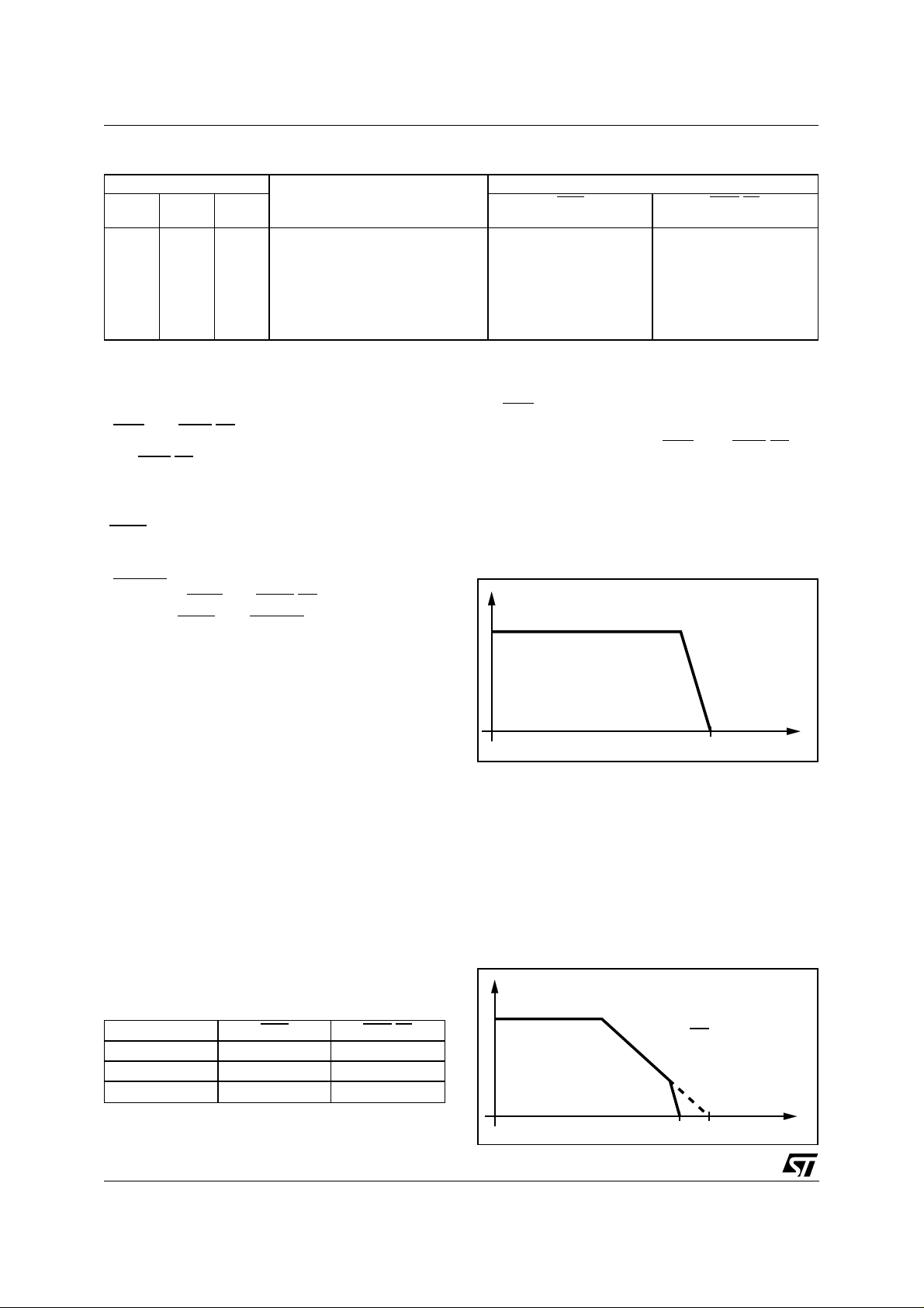
ble); feeding characteristic shown in fig. a.
The voltage drop in on-hook condition is 7.8V.
Figure a: STLC30R80 DC Characteristic in
Stand-By Mode.
I
16mA
R
= 2R
D98TL307
FEED
V
BAT
P
-7.8V
Active
Mode selected to allow voice signal transmission.
When in ACTIVE mode the voltage drop in onhook condition is 7.8V in order to allow proper onhook transmission (Fig. b).
Resistive Region is programmable by means of
external resistor R
lected by R
LIM
and R
, limiting current can be se-
DC
resistor.
switch
Figure b. STLC30R80 DC Characteristic in
Active M o de.
I
I
[20÷50mA]
LIM
D99TL435
R
FEED
R
= 2R
FEED
P
V
BAT
=
R
-7.8V
DC
+2R
P
5
V
BAT
V
V
4/13
 Loading...