

SUBSCRIBER LINE INTERFACE CIRCUIT
MONOCHIP SLIC SUITABLE FOR PUBLIC
APPLICATIONS
IMPLEMENTES ALL KEY FEATURES OF
THE BORSHTFUNCTION
DUALCONTROL MODE CONFIGURATION:
SLAVE MODE OR AUTOMATIC ACTIVATION
MODE.
SOFT BATTERY REVERSAL WITH PROGRAMMABLETRANSITION TIME
ON HOOKTRANSMISSION
LOOP START/GROUND START FEATURE
WITH PROGR.THRESHOLD
LOW POWER DISSIPATION IN ALL OPER-
ATING MODES
AUTOMATIC DUAL BATTERY OPERATION
INTEGRATED RING TRIP DETECTION WITH
AUTOMATIC AND SYNCRONISED RING
DISCONNECTION
METERING PULSE INJECTION
SURFACEMOUNT PACKAGE
THREE RELAY DRIVERS FOR RING AND
TESTING
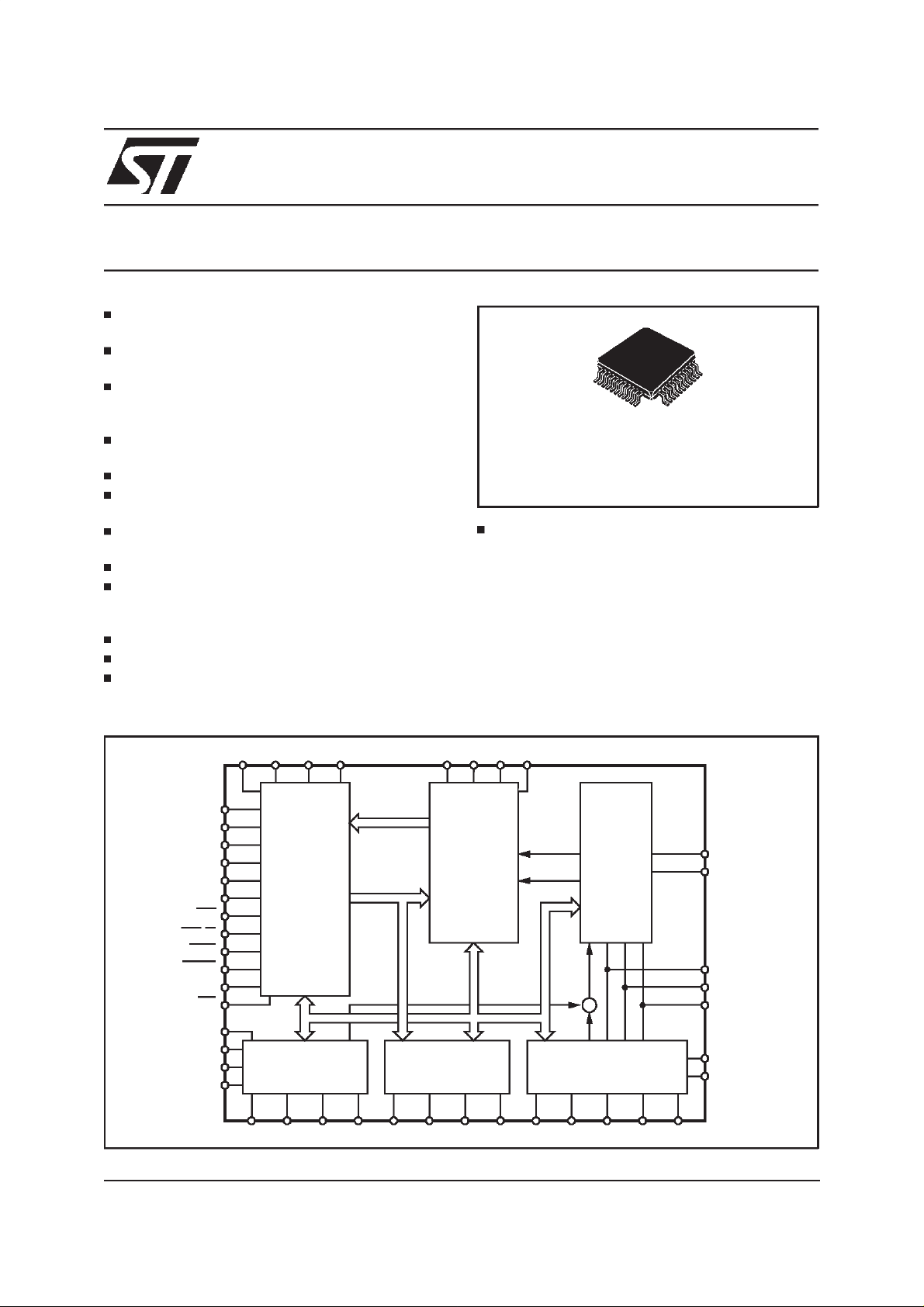
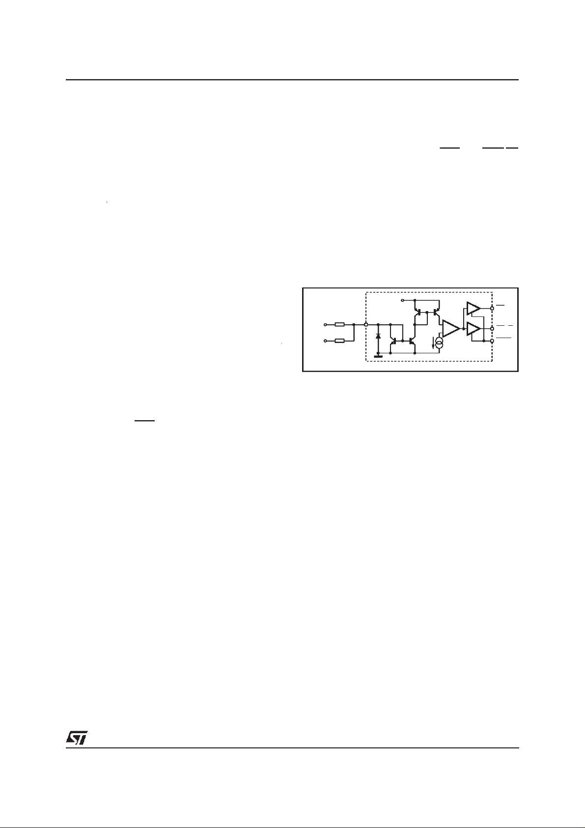
BLOCK DIAGRAM
STLC3080
PRELIMINARY DATA
TQFP44 (10 x 10)
ORDERING NUMBER: STLC3080
-40 TO +85°COPERATINGRANGE
DESCRIPTION
The STLC3080 is a SLIC device suitable for a
wide range of applications: public (CO), transmission (DLC) and private (PABX). The SLIC provides the standard battery feeding with full programmability of theDC characteristic.In particular
two external resistors allow to set the limiting current value (up to 50mA) and the value of the resistive feeding when not in constant current region.
REL1
RELRREL0
MODE
D0
D1
D2
R0
R1
DET
GDK/AL
CSIN
CSOUT
CKRING
RES
TTXIN
ZB
TX
RX
ZAC1
LOGIC
INTERFACE
&
DECODER
AC
PROCESSOR
RSZAC IREF V
RGND
LINE STATUS
COMMANDS
REFERENCE
BIAS SWITCHING
CAC AGND CREV CSVR
RT1 RT2CRT
SUPERVISION
&
V
CC
DD
PCD
ILT
ILL
AC+
DC
AC
DC
December 1999
This is preliminary information on a new product now indevelopment or undergoing evaluation.
LINE
INTERFACE
+
DC
PROCESSOR
VBAT BASE RDC
TIP
RING
BGND
VREG
ILTF
RLIM
RTH
D98TL305B
1/23
STLC3080
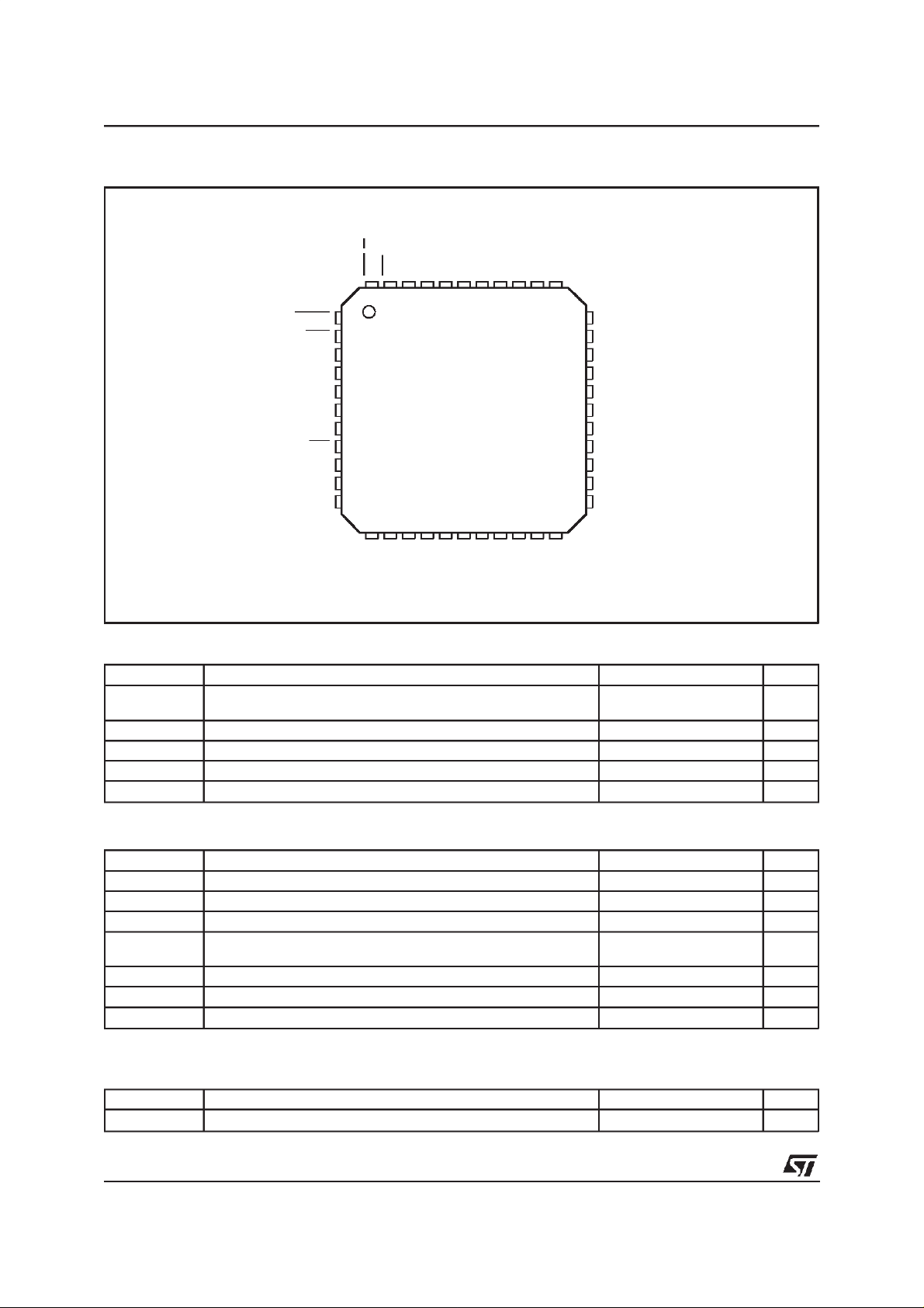
PIN CONNECTION
CSOUT
CSIN
D0
D1
D2
R0
R1
RES
VDD
VCC
CRT
BGND
RING
TIP
PCD
MODE
CKRING
DET
GDK/AL
44 43 42 41 3940 38 37 36 35 34
1
2
3
4
5
6
7
8
9
10
RELR
RGND
VBAT
171118 19 20 21 22
TX
ZB
RS
12 13 14 15 16
REL1
REL0
VREG
ZAC
BASE
ZAC1
CSVR
33
32
31
30
29
28
27
26
25
24
23
RX
CREV
IREF
RLIM
RTH
AGND
RT1
RT2
ILTF
RDC
CAC
TTXIN
D98TL306A
ABSOLUTE MAXIMUM RATINGS
Symbol Parameter Value Unit
V
V
V
I
BAT
CC
DD
REL
Battery voltage -80 + VCCto +0.4
-80 + V
REL
to + 0.4
Positive supply voltage -0.4 to +7 V
Control Interface Supply Voltage -0.4 to +7 V
Current into relay drivers 80 mA
A/R/BGND AGND respect BGND respect RGND -2 to +2 V
OPERATINGRANGE
Symbol Parameter Value Unit
T
opT
V
CC
V
DD
V
BAT
Operating temperature range -40 to +85 °C
Positive supply voltage 4.75 to 5.25 V
Control Interface Supply Voltage 3 to 5.25 V
Battery voltage
if VREL > V
CC
-73 to -15
-78+ V
REL
to -15
A/R/BGND AGND respect BGND respect RGND -0.3 to +0.3 V
PD (70) Max. power dissipation @ Tamb = 70°C 1.1 W
PD(85) Max. power dissipation @ Tamb = 85°C 0.9 W
THERMAL DATA
V
V
V
V
Symbol Parameter Value Unit
R
th j-amb
Thermal resistance Junction to Ambient Typ. 60 °C/W
2/23

STLC3080
PIN DESCRIPTION
Pins Name Description
1 CSOUT Chip-Select for output control bits DET and GDK . Active Low. (*)
2 CSIN Chip-Select for input control bits latches D0 D1 D2 R0 R1 . Active Low. (*)
3 D0 Control Interface inputbit 0. (*)
4 D1 Control Interface inputbit 1. (*)
5 D2 Control Interface inputbit 2. (*)
6 R0 Relay driver 0 command. Active High. (*)
7 R1 Relay driver 1 command. Active High. (*)
8 RES Reset Input; active low.
9V
10 V
DD
CC
11 CRT Ring-Triptime constant capacitor.
12 REL1 Relay 1 driver output.
13 REL0 Relay 0 driver output.
14 RELR Ringer Relay driver output.
15 RGND Relay drivers ground.
16 V
BAT
17 TX 4 wires outputstage (Transmitting Port).
18 ZB Cancelling input of Balance Network for 2 to 4 wires conversion.
19 RS Protection resistors image. The image resistor is connected between this node and ZAC.
20 ZAC AC impedance synthesis.
21 ZAC1 RX buffer output/ AC impedance is connected between this node and ZAC.
22 RX 4 wires inputstage (Receiving Port). A 100K externalresistor must be connected to AGND to
23 TTXIN Metering SignalInput (AC) andLine Voltage DropProgramming(DC). If notusedmustbe connectd
24 CAC AC feedback input/ AC-DC split capacitor is connected between this node and ILTF.
25 RDC DC current feedback input. The RDC resistor is connected between this node and ILTF.
26 ILTF TransversalLine Current Image.
27 RT2 Input pin to sense ringing current , for Ring-Trip detection.
28 RT1 Input pin to sense ringing current , for Ring-Trip detection.
29 AGND Analog ground.
30 RTH Off-Hook threshold programming pin.
31 RLIM Limiting current programming pin.
32 IREF Voltage reference output to generate internal reference current.
33 CREV Reverse polarity transition time programming.
34 CSVR Battery supply filter capacitor.
35 BASE Driver ofthe external transistor. Connected to the base.
36 VREG Regulated voltage. Provides the negative supply to the power line drivers. It is connectedto the
37 BGND Battery ground.
38 RING B wire termination output. IB is the current sunk into this pin.
39 TIP A wire termination output. IA is the current sourced from this pin.
40 PCD Power Cross Detection Input
41 MODE InterfaceControl Mode selection.
42 CKRING Clock at ringing frequency for relay synch and time reference for Automatic activation
43 DET Off-hook and Ring-Trip detection bit. Tri-State Output/Active Low.
44 GDK/ AL Ground-Key/Alarm detection bit. Tri-State Output. Active Low.
* Input pins provided with 15µA sink toAGND pull-down.
Control interface Power Supply. VDD= 3.3V orVDD=VCC.
Positive Power Supply (+5V).
Negative Battery Supply.
bias the input stage.
toAGND.
emitter of the external transistor.
3/23
STLC3080
CONTROLINTERFACE
Slave mode (MODE=Low).
INPUTS
R0 R1 D0 D1 D2
X
X
X
X
X
X
X
X
0/1
X
X
X
X
X
X
X
X
X
X
0/1
0
0
0
0
1
1
1
1
X
X
0
0
1
1
0
0
1
1
X
X
X
X
0
1
0
1
0
1
0
1
OPERATING MODE
Power down
Stand-by
Active N.P.
Active R.P.
Ringing (with SLIC Active N.P.)
Ringing (with SLIC Active R.P.)
Ground start
High Impedance Feeding
Rel 0 (on = 1, off = 0)
Rel 1 (on = 1, off = 0)
A parallel interface allow to control the operation
of STLC3080through a control bus:
- D0 D1 D2 latched input bits definingtheSlic
operationmode
- R0 R1 latched input bits (activeHigh) drive the
testrelays.
- DET and GDK/AL , tri-state outputs, signal the
statusofthe loop:On/Off-Hookand Ground-Key.
PinGDK/AL goeslow also whenthe device
thermal protectionis activatedor a linefault(Tip to
Ring,Tip and/orRingto Groundor VBAT)is
detected(flowing current≥7.5mA).
-CSIN: chipselect for input bits, active Low,
strobesthe data present on the control bus into
theinternal latch.
- CSOUT: chipselect for outputbits; activeLow,
whenhigh DET and GDK/AL goes tri-state.
D0 D1 D2 R0 R1 CSIN and CSOUT inputsare
provided with a 15µA pull-down current to prevent
uncontrolled conditions in case the control bus
goes floating.
According to theabove table, 8 operating modes
can be set:
1) Power-Down.
2) Stand-By.
3) ActiveN.P.
4) ActiveR.P.
5) Ringing(with SLIC Active N.P.).
6) Ringing(with SLIC Active R.P.).
7) Groundstart.
8) HighImpedanceFeeding.
Power-Down
It’s an idle state characterised by a very low
power consumption; any functionalityis disabled;
only relays Rel0 and Rel1 can be driven by
proper settingof bitsR0 and R1.
It can be set during out of service periods just to
OUTPUTS
DET
(Active Low)
disable
off/hk
off/hk
off/hk
ring/trip
ring/trip
off/hk
off/hk
def by D0-D2
def by D0-D2
GDK/AL
(Active Low)
disable
gnd-key
gnd-key
gnd-key
disable
disable
gnd-key
disable
def by D0-D2
def by D0-D2
reducethe power consumption.
It is worth noticing that two other conditions can
set the Slic in idle state but with somedifferences
as reportedin the table:
Idle State Rel0/1 Drive DET GDK/AL
Power Down Enable Disable Disable
Reset Disable Disable Disable
Thermal
Alarm
Enable Low Low
Stand-By.
Mode selected in On-Hook condition when high
immunity to common mode currents is needed for
the DET bit.
To reducethe current consumption, AC feedback
loop is disabled and only DET and GDK/AL detectorsare active.
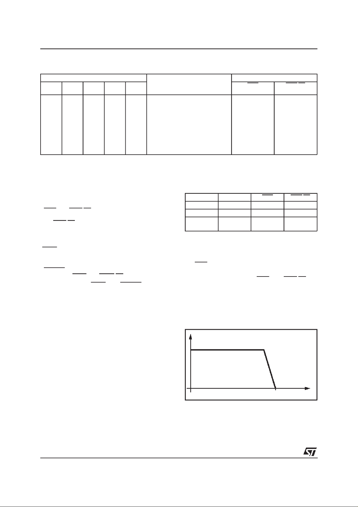
DC current is limited at 16mA (not programmable); feedingcharacteristicshown in fig.a.
The voltage drop in on-hook conditionis 7.8V.
Figurea: STLC3080 DC Characteristicin
Stand-ByMode.
I
16mA
R
=2R
D98TL307
FEED
V
BAT
-7.8V
P
V
Active
Mode selected to allow voice signal transmission.
When in ACTIVE mode the voltage drop in onhook condition is 7.8Vin orderto allowproper onhook transmission(Fig. b).
4/23
STLC3080
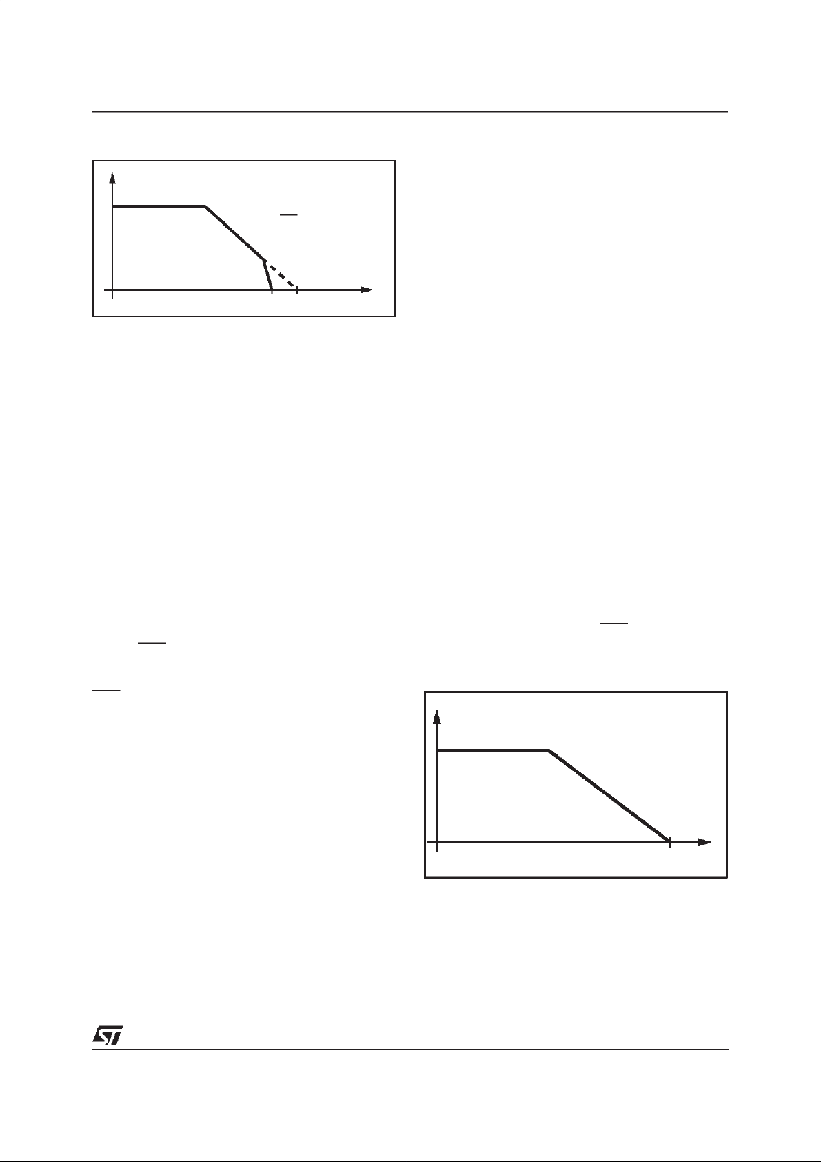
Figure b. STLC3080DC Characteristicin
ActiveMode.
I
I
[20÷50mA]
LIM
R
R
=2R
FEED
FEED
V
P
BAT
=
-7.8V
R
DC
+2R
P
5
V
BAT
V
Resistive Region is programmable by means of
external resistor R
lected by R
LIM
, limiting current can be se-
DC
resistor.
Concerning AC characteristic the STLC3080 allows
to set 2W terminationimpedance by meansof one
external scaled impedance that may be complex.
Two to four wire conversion isprovidedby an external network.Such network can be avoidedin case
of applicationwith COMBOII,in this casethe two to
four wire conversion is implemented inside the
COMBOII by means of the programmableHybal filter.
When in ACTIVE mode it is also possible to perform battery reversal in soft mode (with programmable transition time) without affectingthe AC signaltransmission.
Ringing
When Ringing mode is selected the STLC3080
activates the ring relay injectingthe ringing signal
on the line. As the ring trip is detectedthe logic indicator DET is set low and the ringing is automatically disconnected without waiting for the card
controllercommand (auto ring trip).
DET remains latched Low untill the operative
mode is modified.
If required , the ringing relay drive signal RELR
can be synchronised to a clock applied to
CKRINGinput.
This clock is derived from the ringing signal with
proper time delay, according to the activation/deactivationtime of the relay.
RELR is activated on the low level of CKRING
clock. The duty cycleof CKRING can be modified
in order to activate the RELR when required:
CKRINGlow must last 1µs minimum.
If the synchronisation is not required, CKRING input must be steadily kept Low.
All the STLC3080 relay drivers are open drain
with the source connectedto theRGND pin. Each
relay drivers integrates a protection structure that
allows to avoid external kick - back diodes,using
both 5Vor 12V relays.
The ring trip circuit and its behaviour is described
in AppendixD.
Ground Start.
This mode is selected when the SLIC is adopted
in a system using the Ground Start feature. In this
mode the TIP termination is set in High Impedance (100kΩ) while the RING one is active and
fixed at Vbat +4.8V. In the case of connection of
RING termination to GND the sinked current is
limited to 30mA. When RING is connected to
GND both Off-Hook and Ground-Key detectors
become active. Power dissipation in this mode
with a -48Vbattery voltage is 100mW
High Impedance Feeding.
As Stand-By, this mode is set in On-Hook condition, with furtherreducedpower consumption.
Higher power efficiency turns back a lower immunity of the Off-Hook detector to line common
modecurrents.
The DC feeding shows a constant current characteristic (I
with an equivalent series resistance R
= 17mA) followed by a resistive range
lim
FEED
1600Ω+ 2Rp.
Thermal protection circuit is still active, preventing
the junction temperature, in case of fault condition, to exceed150°C
In High Impedance Feeding most of the circuit is
switched off, only the circuit, dedicated to OffHook detection, is powered. This allows to reduce
the total power consumptionin On-hookto 30mW
(typical).
The Off-Hook detection threshold is not programmablebut defined at a fixed IDET
= 8mA(max.)
HI
Figurec. STLC3080 DC Characteristicin High
ImpedanceFeeding
I
17mA
D98TL373
R
FEED
= 1600Ω +2R
V
BAT
P
-0.8V
=
V
5/23

STLC3080
CONTROLINTERFACE
Automatic activation mode (MODE=High).
Inputs Operating Mode
R0 R1 D0 D1 D2
X X 0 0 0 1 Power Down disable disable
X X 0 0 1 1 Ringing Ring-Trip disable
X X 0 1 0 1 On-Hook Transmission
X X 0 1 1 1 On-Hook Transmission
X X 1 0 0 1 Active Direct Polarity
X X 1 0 1 1 Active Direct Polarity
X X 1 1 0 1 Active Reverse Polarity Off_Hook
X X 1 1 1 1 Active Direct Polarity
0/1 X X X X 1 R0 = 0/1: Rel0 = off/on (1) (1)
X 0/1 X X X 1 R1 = 0/1: Rel1 = off/on (1) (1)
XXXXX0Power Down; Rel0/1= off disable disable
DET: On/OffHook Signalling; togetherwith GDK/AL it is set Low also in case of Thermal Alarm or Ground-Key.
GDK/AL : Thermal Alarm or Ground-Key Signalling
(1) : DET and GDK/AL signallingfunction is relatedto D0,D1,D2 and it doesn’t depend on R0 and R1 setting.
RES DET GDK/AL
As in Slave mode the control is performed
through a parallel bus, with independent chip selects, CSIN and CSOUT, for inputs and outputs.
In Automatic Activation, once Active mode is selected the device automatically selects the proper
operating mode (Active,Stand By or H.I. feeding)
depending on the loop status in order to optimise
the power consumption.
In order to guaranteethe proper behaviour of the
internal state machine the ”CKRING” signal must
be always applied,this signalin fact is used to generatethe ”WTIME” delay(see Appendix)necessary
to properlyperformautomaticstatechange.
Power-Down
It’s an idle state characterised by a very low
power consumption; any functionalityis disabled;
only relays Rel0 and Rel1 can be driven by
proper settingof bitsR0 and R1.
It can be set during out of service periods just to
reduce the power consumption.
(Mode = High)
Off-Hook
Reverse Polarity
Off_Hook
Direct Polarity
Off_Hook
(default)
Off_Hook
(default)
Off_Hook
(default)
As a Ring-Trip is detected the logic indicator DET
is set Low and the ringing relay is automatically
switched-off without waiting for the card controller command(auto ring-trip).
DET remains latched Low until the operative
modeis modified.
Ringingrelay drive signal RELR must be synchronised to a clock applied to CKRING input. This
clock is derived from the ringing signal with
proper time delay, according to the activation /
deactivationtime of the relay.
RELR is activated on the low level of CKRING
clock. The duty cycle of CKRING can be modified
in order to activate the RELR when required:
CKRINGlow must last 1µs minimum.
All the relay drivers are open-drain with the
sourceconnectedto RGNDpin.
Each relay driver integrates a protectionstructure
to avoid external kick-back diodes using both 5V
or 12V relays.
The ring trip circuit and its behaviouris described
in AppendixD.
Outputs
Fault
Fault
Fault
Fault
Fault
Fault
It is worth noticing that two other conditions can
set theSlic in idle state but with some differences
as reported in the table:
Idle State Rel0/1 Drive DET GDK/AL
Power Down Enable Disable Disable
Reset Disable Disable Disable
Thermal
Alarm
Enable Low Low
On-HookTransmission.
Sets the Slic for conversation even thoughthe line
is in On-Hook; it is required for On/Hooktransmission purposes; Active mode cannot supporta conversationwhenthe lineis in On-Hookasit automatically turns in High ImpedanceFeeding.
Active.
Ringing
When Ringing mode is selected the STLC3080
activatesthe ringing relay injecting the ringing signal on the line.
6/23
The relevant feature of this setting is that when
Active Mode (D0D1D2=1XX) is set by the external control , internally, the device is ableto select
between three operative states according to the
statusof the line:
Fault
Fault
Fault
Fault
Fault
Fault
STLC3080
- High Impedance Feeding :
entered aftera Power-On Resetor 1XX word, this
statusis setduringsteadyOn/Hookcondition;
most of the circuitry is idle and only a low power
Off-Hookdetection circuit iskept alive.
Direct Polarity only is assumed , independentlyof
the selectedone.
To minimisethepowerconsumptiontheOff-Hookde-
tectioncircuithaslowcommonmodecurrentrejection.
-Standby
Notice that in Stand-Bystate theOff-Hook detec-
tor is sensitive only to the transversal component
of the line current with high immunity to common
mode disturbances; this performance implies an
increasing in power consumption: for that reason
Stand-Byis notused as a quiescent state.
- Active state gets operative for conversation after an Off-Hook validity check performed in
Stand-Bystate, set after any Off-Hook detected in
High ImpedanceFeeding.
If the Off-Hook condition is confirmedin StandBy,
Active mode is set ; if not (in case of spuriousdetection), false activation is prevented, and High
ImpedanceFeeding is resumed.
In order to havethe device falling back in HI-feeding mode after the line is back in on-hook condition. It is necessaryto selectas input state the active direct polarity mode (default).
During Active state On/Off-Hook status will affect in real time DET signalling bit.
In order to allow Pulse-Mode Dialling, once Active state is set, it cannot be changed by fast OnHook , but it is turned back to High Impedance
Feeding only if an On-Hook condition lasts
longer than 128 x CKRING period.
Automatic activation (and deactivation) is based
on an internal state-machine which is clocked by
a freerunninginternal oscillator.
A detaileddescriptionis reportedin the AppendixA.
DUAL BATTERY CONFIGURATION
STLC3080 is also meant for low power consumption systems using Dual Battery solution. It is sufficient to connectthe collector of the external transistor, through a diode, to the reduced battery
(see Fig. 2 for single battery solution and Fig. 3
for dual battery solution). The activation of the
batteries is automatic, only depending on the DC
load at the RING and TIP terminals; no controllers
action is required.
PROTECTIONCIRCUIT
- Suggested protection circuit is based on programmable Trisils (like LCP1511/2) as shown
in Fig.2 and Fig. 3, and the surge current is
limited by the resistors RPT2 and RPR2, which
are PTC types , protecting the device against
both lightningand power-cross.
- Additionally, STLC3080 is provided with the
PCD input to directly monitor overvoltages applied to the line wires.
When the current injected into PCD exceeds a
threshold of 320µA (+/- 30%) , DET and GDK/AL
are set Low signalling a fault condition. No
change on theSLIC mode is performed.
Voltage threshold is defined by proper value of
the series resistors (see Fig.1)
This circuit gives the possibility to protect the device against power crosses through a relay instead of PTCs; once the fault condition is detected the controller drives this relay
disconnectingthe Slic from the line terminals.
METERINGPULSE INJECTION
Figure1.
TIP
RING
VCC
R
PCD
R
Ith
DET
GDK/AL
CSOUT
D98TL385
STLC3080 provides external pins and components for Metering Pulse injection. TTXIN pin is
the input for the 12kHz or 16kHz Metering Pulse
injection. This pin also provides a DC constant
current source that is injected into the external
RDA resistor (typ. 10kΩ to obtain 2.2Vrms on
200Ω) connected between TTXIN pin and AGND.
The voltage drop across TIP and RING line amplifiers and, consequentallythe AC swing available.
When Metering Pulse injection is not used and
voltage drop is not required, TTXIN must be
shorted to AGND and RTTX, RDA and CTTX external components must be removed. The TTX
cancellation is obtained through an external
RTTX and CTTX network connected between
TTXIN and CAC pins.
Fault detection
The device provides current sense on TIP and
RING wires that allow to detect longitudinal DC
current (I
). When this ILLcurrent becomes
LL
higher than a threshold (see detectors table inside electrical characteristics) a fault indication is
provided on DET and GDK pin (both outputs become low). The fault indication is active till the
fault cause persists. With this circuit the following
fault condition can be detected.
TIP to VB1
TIP to GND
RINGto VB1
RINGto GND
RINGto TIP to VB1
7/23
 Loading...