

SGS Thomson Microelectronics STLC3065QTR, STLC3065Q Datasheet
WLL SUBSCRIBER LINE INTERFACE CIRCUIT
MONOCHIPSLIC OPTIMISEDFOR WLL APPLICATIONS
IMPLEMENT ALL KEY FEATURES OF THE
BORSHTFUNCTION
SINGLESUPPLY(5.5TO 15.8V)
BUILT IN DC/DC CONVERTER CONTROL-
LER.
SOFT BATTERY REVERSAL WITH PRO-
GRAMMABLE TRANSITIONTIME.
ON-HOOKTRANSMISSION.
PROGRAMMABLE OFF-HOOK DETECTOR
THRESHOLD
METERING PULSE GENERATION AND FIL-
TER
INTEGRATEDRINGING
INTEGRATEDRING TRIP
DUAL 2W PORT FOR DATA/VOICE OPERA-
TION
PARALLEL CONTROL INTERFACE (3.3V
LOGICLEVEL)
PROGRAMMABLE CONSTANT CURRENT
FEEDER
SURFACE MOUNTPACKAGE
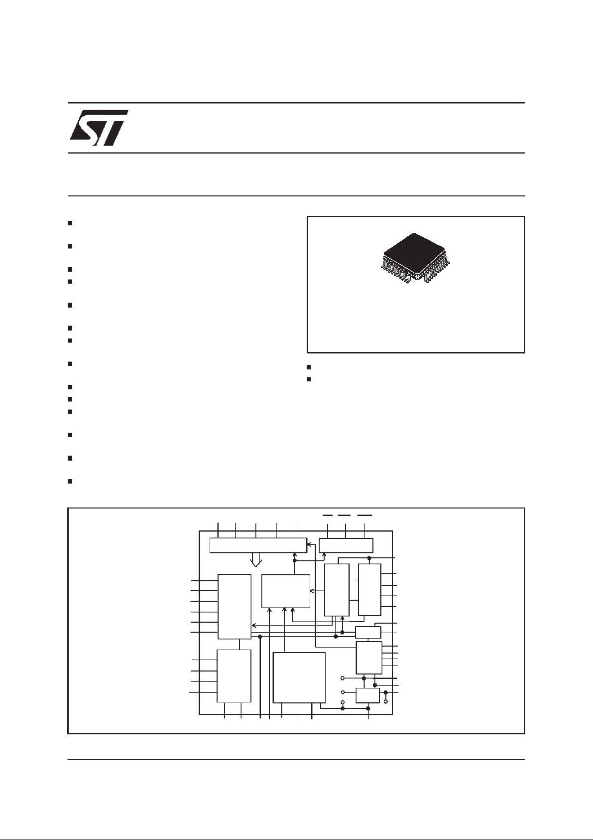
BLOCKDIAGRAM
STLC3065
TQFP44
ORDERING NUMBERS:
INTEGRATEDTHERMAL PROTECTION
-40 TO +85°COPERATING RANGE
DESCRIPTION
The STLC3065 is a SLIC device specifically designed for WLL (Wireless Local Loop) application.
One of the distinctive characteristics of this device is the ability to operate with a single supply
voltage (from +5.5V to +15.8V)and self generate
the negative battery by means of an on chip
DC/DCconvertercontrollerthatdrivesan external
STLC3065Q
STLC3065QTR
October 1999
TX
RX
ZAC1
ZAC
RS
ZB
CKTTX
CTTX1
CTTX2
FTTX
D0 D1 D2 P1 P2 DET DET1 DET2
INPUT LOGICAND DECODER
Status andfunctions
SUPERVISION
AC PROC
TTX PROC
RTTX CAC ILTF RD IREF RLIM RTH
REFERENCE
OUTPUT LOGIC
LINE
DRIVER
Vcc
Vss
Agnd
LINE
SWITCH
DC PROC
DC/DC
CONV.
VOLT.
REG.
AGND
Vbat
BGND
TIP1
TIP2
RING1
RING2
CREV
CSVR
CLK
RSENSE
GATE
VF
CVCC
VPOS
VBAT
1/27
STLC3065
DESCRIPTION
(continued)
MOSswitch.
The self generated battery voltage tracks the line
resistance. In this way the power dissipation inside the device is low enough to allow the use of
smallSMD package(TQFP44).
Other useful characteristics for application in the
WLL environment are the integratedringing generator and the dual two wire port that allows to
drive two different terminal equipment whether
the transmission is voice or data. When one port
is transmittingtheotherone is idle.
The control interface is a parallel type with open
drainoutput and 3.3V logiclevels.
The metering pulses are generated on chip starting from two logic signals (0, 3.3V) one defines
the metering pulse frequency and the other the
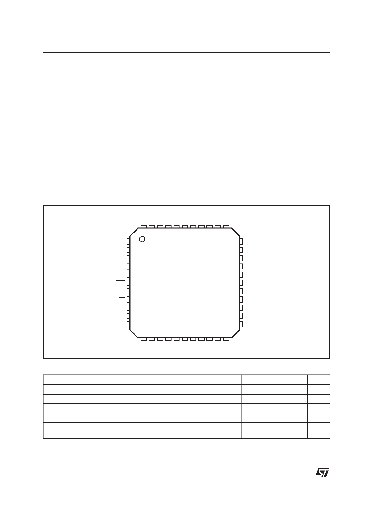
PIN CONNECTION
VBAT1
CREV
TIP2
TIP1
44 43 42 41 3940 38 37 36 35 34
1
D0
2
D1
3
D2
4
P1
5
P2
6
DET1
7
DET2
8
DET
9
CKTTX
CTTX1
10
CTTX2
12 13 14 15 16
metering pulse duration. An on chip circuit then
providesthepropershapingand filtering.
Meteringpulse amplitudeand shaping (rising and
decay time)can be programmedby externalcomponents. A dedicated cancellation circuit avoid
possible CODEC input saturationdue to Metering
pulse echo.
Constant current feed can be set from 20mA to
40mA.
Off-hook detection threshold is programmable
from5mA to 9mA.
The device, developed in BCD100II technology
(100V process), operates in the extended temperature range and integrates a thermal protection that set the device in power down when Tj
exceeds140°C.
N.C.
N.C.
N.C.
RING1
RING2
VBAT
BGND
33
CSVR
32
ILTF
31
RD
30
RTH
29
IREF
28
RLIM
27
AGND
26
CVCC
25
VPOS
24
RSENSE
23
GATE
171118 19 20 21 22
RTTX
FTTX
ZB
RX
ZAC1
ZAC
RS
CAC
TX
D96TL273B
VF
CLK
ABSOLUTEMAXIMUM RATINGS
Symbol Parameter Value Unit
V
pos
A/BGND AGND to BGND -1 to +1 V
V
dig
T
j
(1)
V
btot
(1) Vbat is self generated bytheon chip DC/DC converter and can be programmed via RF1 and RF2.
RF1andRF2 shall beselectedinorder tofulfil the a.m limits (see External Components Table page 13)
2/27
Positive Supply Voltage -0.4 to +17 V
Pin D0, D1, D2, P1,P2, DET, DET1, DET2 CKTTX -0.4 to 5.5 V
Max. junction Temperature 150 °C
Vbtot=|Vpos|+|Vbat|. (Total voltage applied to the device
100 V
supply pins).

STLC3065
OPERATINGRANGE
Symbol Parameter Value Unit
V
pos
A/BGND AGND to BGND -100 to +100 V
V
dig
T
op
(1)
V
bat
(1) Vbat is self generated bytheon chip DC/DC converter and can be programmed via RF1 and RF2.
RF1andRF2 shall beselectedinorder tofulfil the a.m limits (see External Components Table page 10)
THERMALDATA
Symbol Parameter Value Unit
R
thj-amb
PIN DESCRIPTION
N. Name Function
25 VPOS Positive supply inputranging from 5.5V to 15.8V.
34 BGND Battery Ground, must be shorted with AGND.
27 AGND Analog Ground, must be shorted with BGND.
16 ZAC AC impedance synthesis.
15 ZAC1 RX bufferoutput, the AC impedance is connected from this node to ZAC.
17 RS Protection resistors image (the image resistor is connected from this node toZAC).
18 ZB Balance Network for 2 to 4 wire conversion (the balance impedance ZB is connected from this
20 TX 4 wire output port (TX output). The signal is referred to AGND. If connected to single supply
14 RX 4 wire input port (RX input); 300KΩinput impedance. This signal is referred to AGND. If
19 CAC AC feedback input, AC/DC split capacitor (CAC).
32 ILTF Transversal line current image output.
41 TIP1 2 wire port #1; TIP wire (Ia is the current sourced from this pin).
37 RING1 2 wire port #1; RING wire (Ib is thecurrent sunk into this pin).
42 TIP2 2 wire port #2; TIP wire (Ia is the current sourced from this pin)
36 RING2 2 wire port #2; RING wire (Ib is thecurrent sunk into this pin)
28 RLIM Constant current feed programming pin (via RLIM). RLIM should be connected close to this
30 RTH Off-hook threshold programming pin (via RTH). RTH should be connected close to this pin
29 IREF Internal bias current setting pin. RREF should be connected close to this pin and PCB layout
43 CREV Reverse polarity transition time control.One proper capacitor connected between this pin and
26 CVCC Internal positive voltage supply filter.
Positive Supply Voltage 5.5 to +15.8 V
Pin D0, D1, D2, DET, DET1, DET2, CKTTX, P1,P
2
-0.25 to 5.25 V
Ambient Operating Temperature Range -40 to +85 °C
Self Generated Battery Voltage -74 max. V
Thermal Resistance Junction to Ambient Typ. 60 °C/W
node to AGND. ZA impedance is connected from this node to ZAC1).
CODEC input it must be DC decoupled with proper capacitor.
connected to single supply CODEC output it must be DC decoupled with proper capacitor.
pin andPCB layout should avoid noise injection on this pin.
and PCB layout should avoid noise injection on this pin.
should avoid noise injection on this pin.
AGND is setting the reverse polarity transition time. This is the same transition time used to
shape the”trapezoidal ringing” during ringing injection.
3/27
STLC3065
PIN DESCRIPTION (continued)
N. Name Function
35 VBAT Regulated battery voltage self generated by the device via DC/DC converter. Must be shorted
23 GATE Driver for external Power MOS transistor.
21 VF Feedback input for DC/DC converter controller.
22 CLK Power Switch Controller Clock (typ. 125KHz). From version marked STLC3065 A5, this pin
24 RSENSE Voltage input for current sensing. RSENSE should be connected close to this pin and VPOS
1 D0 Control Interface: input bit 0.
2 D1 Control Interface: input bit 1.
3 D2 Control interface: input bit 2.
4 P1 Control Interface: port 1 selection bit
5 P2 Control Interface: port 2 selection bit
8 DET Logic interface output of the supervision detector (active low).
6 DET1 Logic interface output of thr linr port 1 detector (active low)
7 DET2 Logic interface output of thr linr port 2 detector (active low)
33 CSVR Battery supply filter capacitor.
12 RTTX Metering pulse cancellation buffer output. TTX filter network should be connected to this point.
13 FTTX Metering pulse buffer inputthis signal is sent to the line and used to perform TTX filtering.
10 CTTX1 Metering burst shaping external capacitor.
11 CTTX2 Metering burst shaping external capacitor.
9 CKTTX Metering pulse clock input (12 KHz or 16KHz square wave).
44 VBAT1 Frame connection. Must be shorted to VBAT.
38,39,
40
NC Not connected.
to VBAT1.
can also be connected to CVCC or AGND. When the CLK pin is connected to CVCC an
internal auto-oscillation is internally generated and it is used instead of the external clock.
When the CLK pin is connected to AGND, the GATE output is disabled.
pin. The PCB layout should minimize the extra resistance introduced by the copper tracks.
If notused should be left open.
FUNCTIONAL DESCRIPTION
The STLC3065 is a device specifically developed
for WLLapplication.
It is based on a SLIC core, on purpose optimised
for this application, with the addition of a DC/DC
convertercontrollerand a dual port in order to fulfil the WLLrequirements.
The SLIC core performs the standard feeding,
signallingandtransmission functions.
It can be set in three different operating modes
via the D0, D1, D2 pins of the control logic interface (0 to 3.3V logic levels). The loop status is
carried out on the DET pin (active low).The DET
pin is an open drain outputto allow easy interfacing with both 3.3V and 5V logic levels.
The three possible SLIC core operating modes
are:
Power Down (PWD)
4/27
Active
Ringing
Table 1 shows how to set the different SLIC core
operatingmodes.
Table1. SLIC core operating modes.
D0 D1 D2 Operating Mode
0 0 X PowerDown
0 1 0 Active Normal Polarity
0 1 1 Active Reverse Polarity
1 1 0 Active TTX injection (N.P.)
1 1 1 Active TTX injection (R.P.)
1 0 0/1 Ring (D2 bit toggles @ fring)
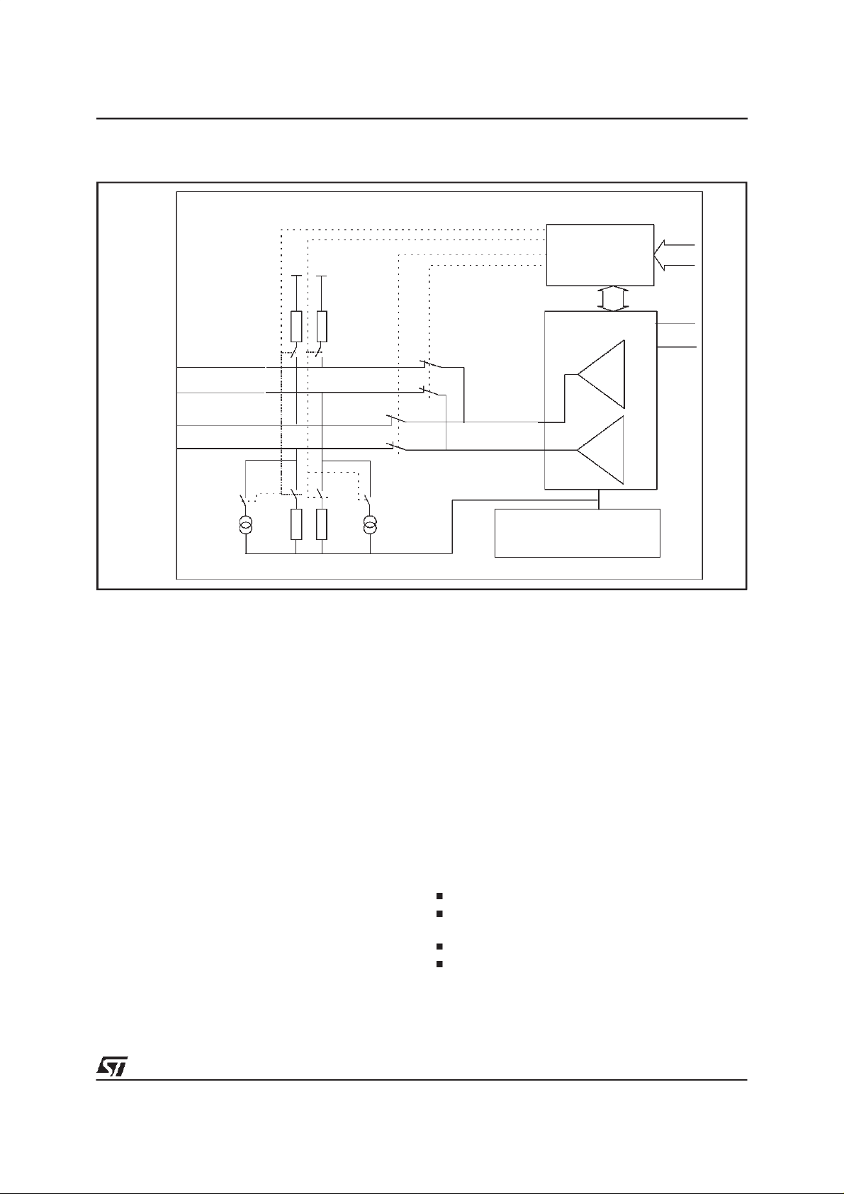
FUNCTIONAL DIAGRAM
STLC3065
CONTROL
INTERFACE
Tip1
Ring1
Tip2
Ring2
SW4R
300µA
SW4T
SW6R
SW3T
SW5R
SW3R
300µA
The STLC3065 operating modes will be obtained
as combination of the SLIC core status and the
dual port configuration.
The DC/DC converter controller is driving an external power MOS transistor(P-Channel)in order
to generate the negative battery voltage needed
for device operation.
The DC/DC converter controller is synchronised
withan externalCLK (125KHztyp.).
From version marked STLC3065 A5, it can be
synchronisedto an internalclockgeneratedwhen
the pin CLK is connected to CVCC. One sensing
resistor in series to Vpos supply allows to fix the
maximumallowedinput peak current.This feature
is implemented in order to avoid overload on
Vpos supply in case of line transient (ex. ring trip
detection).
The typical value is obtained for a sensing resistor equal to 110mΩthat will guarantee an average current consumptionfromVpos < 700mA.
In on-hook condition the self generated battery
voltageis set to a predefinedvalue.
This value can be adjusted via one externalresistor (RF1) and it is typical -50V. When RING mode
is selectedthis value is increasedup to -70Vtyp.
Once the line goes in off-hook condition the
DC/DC converter automatically adjust the generated battery voltage in order to feed the line with
SLIC core
SW1T
SW1T
SW2T
SW2R
DC/DC converter
controller
a fixed DC current(programmable via RLIM) optimisingin this way the power dissipation.
The Dual Port allows to connectthe SLIC core to
one of the two possible 2W ports (TIP1/RING1,
TIP2/RING2).
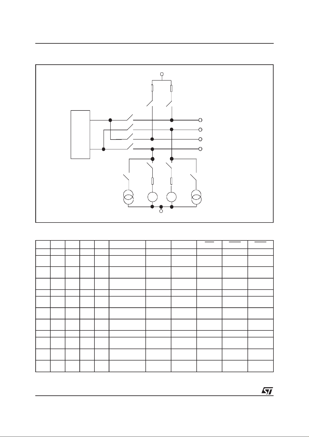
Dual port concept
One switches array integrated in STLC3065 allows to connect the TIP and RING output of the
SLIC core to one of the two 2W ports
(TIP1/RING1 or TIP2/RING2). For special conditions it is also possible to connect both ports to
the SLIC core.The structure of the switches array
is shown in fig.1 and it is controlled via the two
logicinputsP1 and P2.
Depending on the switches configurations each
2W port (TIP1/RING1or TIP2/RING2)can be set
in four possible conditions:
Open
Connected to BGND and Battery via two inte-
grated1.5KΩresistors.
Connectedto the SLIC core
Connected to an internal 300µA (min.) current
source.
Depending on the SLIC core operating modes
(definedby D0,D1 and D2) only a subsetof these
conditionscan be programmed.
TX
RX
5/27
STLC3065
Figure1. Dual Port Concept.
BGND
Tip
Line
Driver
Ring
R1 = 1500ohm
Table2. Dual Portcontrol.
R1
Sw1T
Sw1R
Sw2T
Sw2R
Sw6R
Sw4R
300µA 300µA
R1 R1
R1
Sw4T Sw3T
Is2
VBAT
TIP1
RING1
TIP2
RING2
Sw5R
Sw3R
Is1
LINE1
LINE2
D0 D1 D2 P1 P2 OPER. MODE LINE 1 LINE 2 DET DET1 DET2
0 0 X 0 0 Power Down Open Open - - 0 0 X 1 1 High Z feed. To P.S. via
Res.
0 0 X 0 1 Power Down/
Open To P.S. via
High Z feed.
0 0 X 1 0 High Z feed.
Power Down
To P.S. via
Res.
To P.S. via
Res.
off-hook
line 1+2
off-hook
Res.
Open off-hook
line 2
line 1
off-hook
line 1
- off-hook
off-hook
line 1
off-hook
X 1 X 0 0 ACTIVE 300µA bias 300µA bias - - X 1 X 1 1 ACTIVE To Buffer To Buffer off-hook
--
line 1+2
X 1 X 0 1 ACTIVE 300µA bias To Buffer off-hook
--
line 2
X 1 X 1 0 ACTIVE To Buffer 300µA bias off-hook
--
line 1
1 0 X 0 1 RING 300µA bias 300µA bias - - 1 0 X 1 1 RING To Buffer To Buffer Ring-trip
--
line 1+2
1 0 X 0 1 RING 300µA bias To Buffer Ring-trip
--
line 2
1 0 X 1 0 RING To Buffer 300µA bias Ring-trip
--
line 1
6/27
line 2
line 2
-

STLC3065
Where:
”Open”: the line port termination is in high impedance.
”To P.S. via Res”: the TIP(n) wire is connected to BGND through a 1500Ωresistor , the RING(n) wire is
”To Buffer”: the TIP(n) wire and RING(n) wire are connected to the SLIC core line driver and the off-
”300µA bias”: the TIP(n) wire is connected to BGND through a 1500Ωresistor , the RING(n) wire is
Note: see also Appendix C
connected to VBAT by a 1500Ωresistor. The current flowing in the second resistor is used
to detect the off-hook .
hook detection is performed using the SLIC core supervision circuit that drives the DET
output.
biased by a 300µA current generator to negative battery (Vbat)
Table 2 shows all the possible combinations between switches configurations and operating
modes.
A detailed description of each configuration can
be found in the ”OPERATING MODES” descriptionsection.
OPERATINGMODES
Power Down (PWD)
D0 D1 D2 P1 P2 DET DET1 DET2
0 0 X 0 0 disable disable disable
DC CHARACTERISTIC & SUPERVISION
When this mode is selected both 2W ports
(TIP1/RING1andTIP2/RING2) are in high impedance; all switches Sw1 to Sw6 are open (see
fig.1)
The SLIC core is switched off and the line detectors are disabled therefore the off-hook condition
cannotbe detected.
This mode can be selected in emergency condition when it is necessary to cut any current deliveredto the line.
This mode is also forced by STLC3065in case of
thermaloverload(Tj > 140°C).
In this case the device goes back to the previous
status as soon as the junction temperature decreaseunderthe hysteresisthreshold.
AC CHARACTERISTICS
Both the 2W ports (TIP1/RING1and TIP2/RING2)
are set in highimpedance,the TX outputbufferis
a low impedance output, no AC transmission is
possible.
High ImpedanceFeeding(HI-Z)
D0 D1 D2 P1 P2 DET DET1 DET2
0 0 X 1 1 off/hk
line 1+2
0 0 X 0 1 off/hk
line 2
0 0 X 1 0 off/hk
line 1
off/hk
line 1
disable off/hk
off/hk
line 1
off/hk
line 2
line 1
disable
DC CHARACTERISTIC & SUPERVISION
This operating mode is normally selected when
the telephone is in on-hook in orderto monitorthe
line status keeping the power consumption at the
minimum.
The SLIC core of STLC3065 is in PWD mode
(see fig.1 or FUNCTIONAL DIAGRAM); the two
line series switches (Sw1; Sw2) are open. Depending on P1, P2 the 2W ports (TIP1/RING1
and TIP2/RING2) can be in high impedance or
connected to the built in feeding resistors
(2x1500Ω) via SW3T and SW5R or SW4T and
SW6R.
P1 controls TIP1/RING1 and P2 controls
TIP2/RING2(see Fig.1 and Table2).
When this mode is selectednormallyboth P1, P2
bitsshould be set to one.
The output voltage in on-hook condition is equal
tothe self generatedbatteryvoltage(-50Vtyp).
When off-hook occurs on 2W port 1 (2) the current flowing through the RING1(2) wire activates
the DET1 (2_) detector indicating the line status
change. When DET1 or DET2 are activated also
the DET become active (low logiclevel).
The off-hook threshold in HI-Z mode is the same
value programmedin ACTIVEmode.
The DC characteristic in HI-Z mode is just equal
to the self generated battery with 2x(1500W+Rp)
7/27
STLC3065
in series (see fig.2), where Rp is the external protectionresistance.
It should be noted that in case of both ports in HIZ mode and both of them in off-hookconditionthe
power dissipated inside the chip could drive the
device in thermal protection. This can be prevented via a proper software control that should
avoid to keep as a steady condition both lines in
off-hook and HI-Z mode. Typical operation is to
set the SLIC core in active mode as soon as offhook is detected.
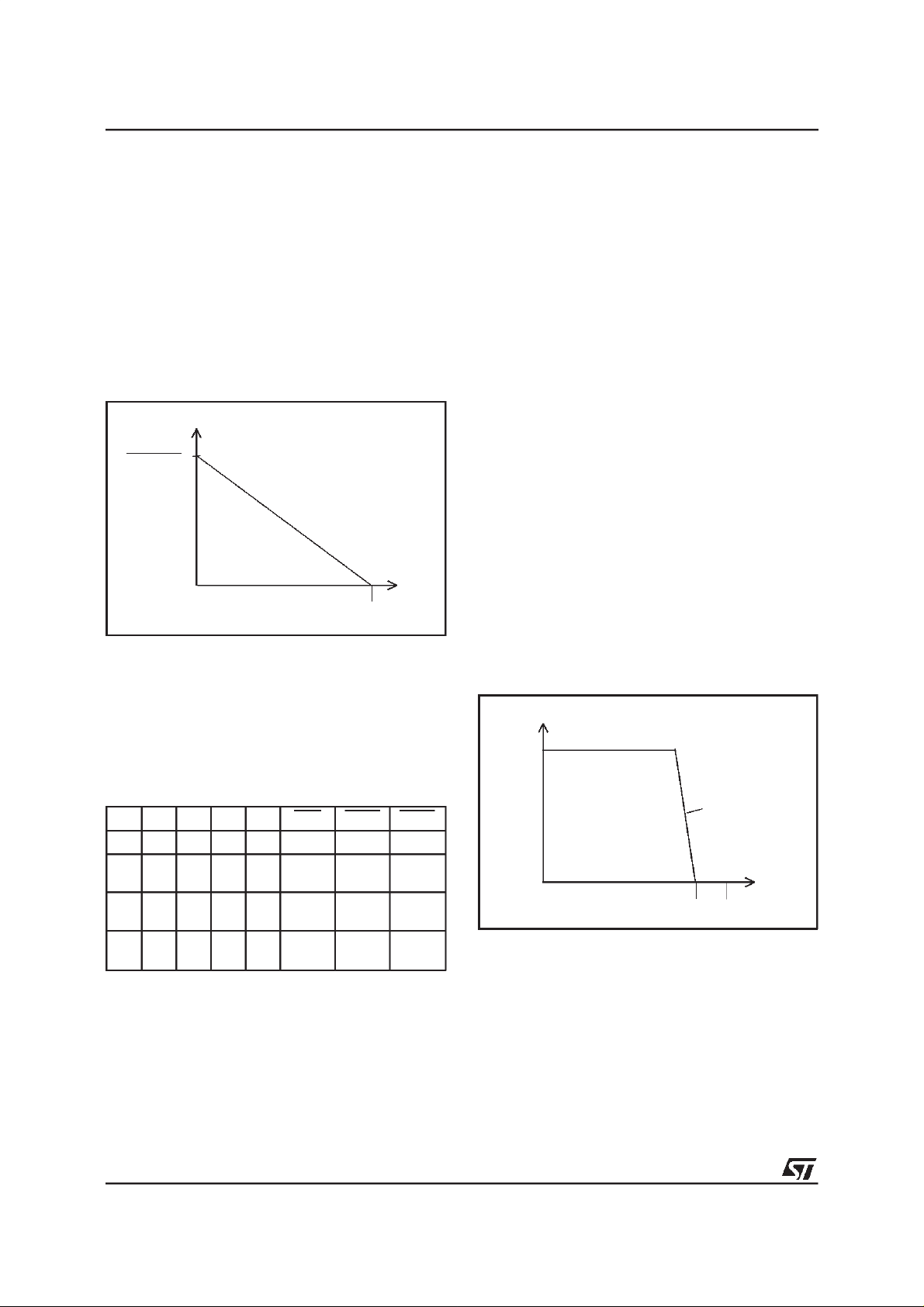
Figure2. DC characteristicin HI-Z mode.
IL
Vbat
2x(R1+Rp)
Slope: 2x(R1+Rp)
(R1=1500ohm)
VL
Vbat (-50V)
AC CHARACTERISTICS
The AC impedance shown at the 2W ports
(TIP1/RING1 and TIP2/RING2) is the same as
the DC one. Depending on the P1, P2 bits the
TIP1/RING1 and TIP2/RING2 AC impedance will
be 2x(1500Ω + Rp) or high impedance.
Active
D0 D1 D2 P1 P2
X 1 X 0 0 disable disable disable
X 1 X 1 1 off/hk
X 1 X 0 1 off/hk
X 1 X 1 0 off/hk
DET DET1 DET2
disable disable
line 1+2
disable disable
line 2
disable disable
line 1
DC CHARACTERISTICS & SUPERVISION
When this mode is selected it is because one
connected telephone goes off-hook and the
STLC3065 is providing both DC feeding and AC
transmission.
The SLIC core is in ACTIVE mode and normally
only one of the two portshould be connected to it:
P1,P2= (1,0) or (0,1). (see Fig.1 and Table 2).
The unselected port is anyway DC biased being
TIP wire connected to BGND via a 1600W resistor and the RING wire connected to a 300mA
(min.)currentsourceconnectedto Vbat.
It should be noted that since Vbat is self generated by the STLC3065 and it is tracking the line
voltage depending on the loop resistance connected to the selected port its voltage can range
typically from -12V to -50V. The unselected port
status (on/off hook) cannot be detected. For special configurations it is also possible to set ACTIVEmode with both port selected(P1,P2=1,1) or
bothunselected(P1,P2=0,0).
Considering now the selected port, this is connected to the SLIC core. The STLC3065 feeds
the line with a constant current fixed by RLIM
(20mA to 40mA range). The on-hook voltage is
typically 40V allowing on-hook transmission; the
selfgeneratedVbatis -52V typ.
If the loop resistance is very high and the line
current cannot reach the programmed constant
currentfeed value, the STLC3065 behaveslike a
40V voltage source with a series impedance
equalto the protection resistors2xRp(typ. 2x41Ω)
plus the line series switches (Sw1 or Sw2)on resistance2xRsw(typ.2x9Ω).
Fig.3 shows the typical DC characteristic in ACTIVEmode.
Figure3. DC characteristicin ACTIVE mode
IL
Ilim
(20 to
40mA)
2Rp+2Rsw
(100ohm typ.)
10V
Vbat (-50V)
VL
The line status (on/off hook) is monitored by the
SLIC core Supervision circuit. The off-hook
threshold can be programmed via the external
resistorRTHin the range from 5mA to 9mA.
When the line goes in off-hook condition the built
in DC/DC converter controller set properly the
Vbatsupplyin order to keep the loop current fixed
tothe programmedvalue.
Independently on the programmed constant current value, the TIP and RING buffers have a currentsourcecapabilitylimited to 70mA typ.
8/27
STLC3065
Moreover the power available at Vbat is controlled by the DC/DC converter that limits the peak
current drawn from the Vpos supply. The maximum allowed current peak is set by the RSENSE
resistorandit istypically900mApk.
AC CHARACTERISTICS
The SLIC core provides the standard SLIC trans-
missionfunctions:
Input impedance synthesis: can be real or
complex and is set by a scaled (x50) external
ZACimpedance.
Transmit and receive:
The AC signal present
on the 2W port (TIP/RING)is transferredto the
TX output with a -6dB gain and from the RX input to the2W port with a 0dB gain.
2 to 4 wire conversion: The balance impedance can be real or complex, the proper cancellation is obtained by means of two external
impedanceZAand ZB.
Once in Active mode (D1=1) the SLIC core can
operatein differentstatessetting properly D0 and
D2 control bits (see also Table3).
D0 D1 D2 Operating state
0 1 0 Active Normal Polarity
0 1 1 Active Reverse Polarity
1 1 0 Active TTX injection (N.P.)
1 1 1 Active TTX injection (R.P.)
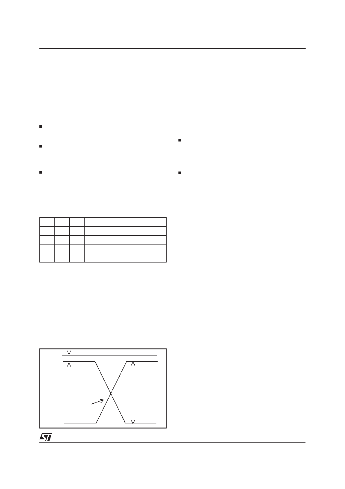
POLARITYREVERSAL
The D2 bit controls the line polarity, the transition
betweenthe two polaritiesis performed in a ”soft”
way. This means that the TIP and RING wire exchange their polarities following a ramp transition
(see fig.4). The transition time is controlled by an
external capacitor CREV. This capacitor is also
setting the shape of the ringing trapezoidal waveform.
Figure4. TIP/RINGtypicaltransition from
Directto Reverse Polarity
GND
TIP
4V typ.
40V typ
ON-HOOK
dV/dT set
byCREV
RING
Whenthe control pins set battery reversalthe line
polarity is reversed with a proper transition time
setvia an external capacitor(CREV).
METERING PULSE INJECTION (TTX)
The metering pulses circuit consist of a burst
shaping generator that gives a square wave
shaped and a low pass filter to reduce the harmonic distortionof theoutput signal.
The metering pulse is obtained starting from two
logicsignals:
CKTTX: is a square wave at the TTX frequency (12 or 16KHz) and should be permanently applied to the CKTTX pin or at least for
all the duration of the TTX pulse (including rising and decay phases).
D0: enable the TTX generation circuit and definethe TTX pulse duration.
This two signals are then processed by a dedicated circuitry integrated on chip that generate
the metering pulse as an amplitude modulated
shaped squarewave(SQTTX) (see fig.5).
Both the amplitude and the envelope of the
squarewave (SQTTX) can be programmed by
means of external components. In particular the
amplitudeis set by the two resistorsRLV and the
shapingbythe capacitorCS.
The waveform so generated is then filtered and
injectedon the line. The low pass filter can be obtained using the integratedbuffer OP1 connected
between pin FTTX (OP1 non inverting input) and
RTTX (OP1 output) (see fig.5) and implementing
a ”Sallen and Key” configuration.
Dependingon the externalcomponentscountit is
possible to build an optimised application depending on the distortion level required. In particular harmonic distortion levels equal to 13%,
6% and 3% can be obtained respectively with
first,secondand third order filters (see fig.5).
The circuit shown in the ”Application diagram” is
relatedto the simple firstorderfilter.
Once the shaped and filtered signal is obtainedat
RTTX buffer output it is injected on the TIP/RING
pins with a +6dB gain.
It should be noted that this is the nominal condition obtained in presence of ideal TTX echo cancellation(obtainedvia proper settingof RTTX and
CTTX). In addition the effective level obtained on
the line will depend on the line impedance, the
protection resistor value and the series switch
(SW1or SW2) on resistance.
In the typical application (TTX line impedance
=200Ω, RP=41Ω, SW1,2 on resistance= 9Ωand
ideal TTX echo cancellation) the metering pulse
level on the line will be 1.33 times the level appliedto the RTTXpin.
9/27
 Loading...