

SGS Thomson Microelectronics STLC3055QTR, STLC3055Q Datasheet
STLC3055
WLL & ISDN-TA SUBSCRIBER LINE INTERFACE CIRCUIT
MONOCHIP SLIC OPTIMISED FOR WLL &
ISDN-TAAPPLICATIONS
IMPLEMENT ALL KEY FEATURES OF THE
BORSHTFUNCTION
SINGLESUPPLY(5.5 TO 15.8V)
BUILT IN DC/DC CONVERTER CONTROL-
LER.
SOFT BATTERY REVERSAL WITH PRO-
GRAMMABLE TRANSITIONTIME.
ON-HOOKTRANSMISSION.
PROGRAMMABLE OFF-HOOK DETECTOR
THRESHOLD
METERING PULSE GENERATION AND FIL-
TER
INTEGRATEDRINGING
INTEGRATEDRINGTRIP
PARALLEL CONTROL INTERFACE (3.3V
LOGICLEVEL)
PROGRAMMABLE CONSTANT CURRENT
FEED
SURFACE MOUNTPACKAGE
INTEGRATEDTHERMALPROTECTION
-40 TO +85°COPERATINGRANGE
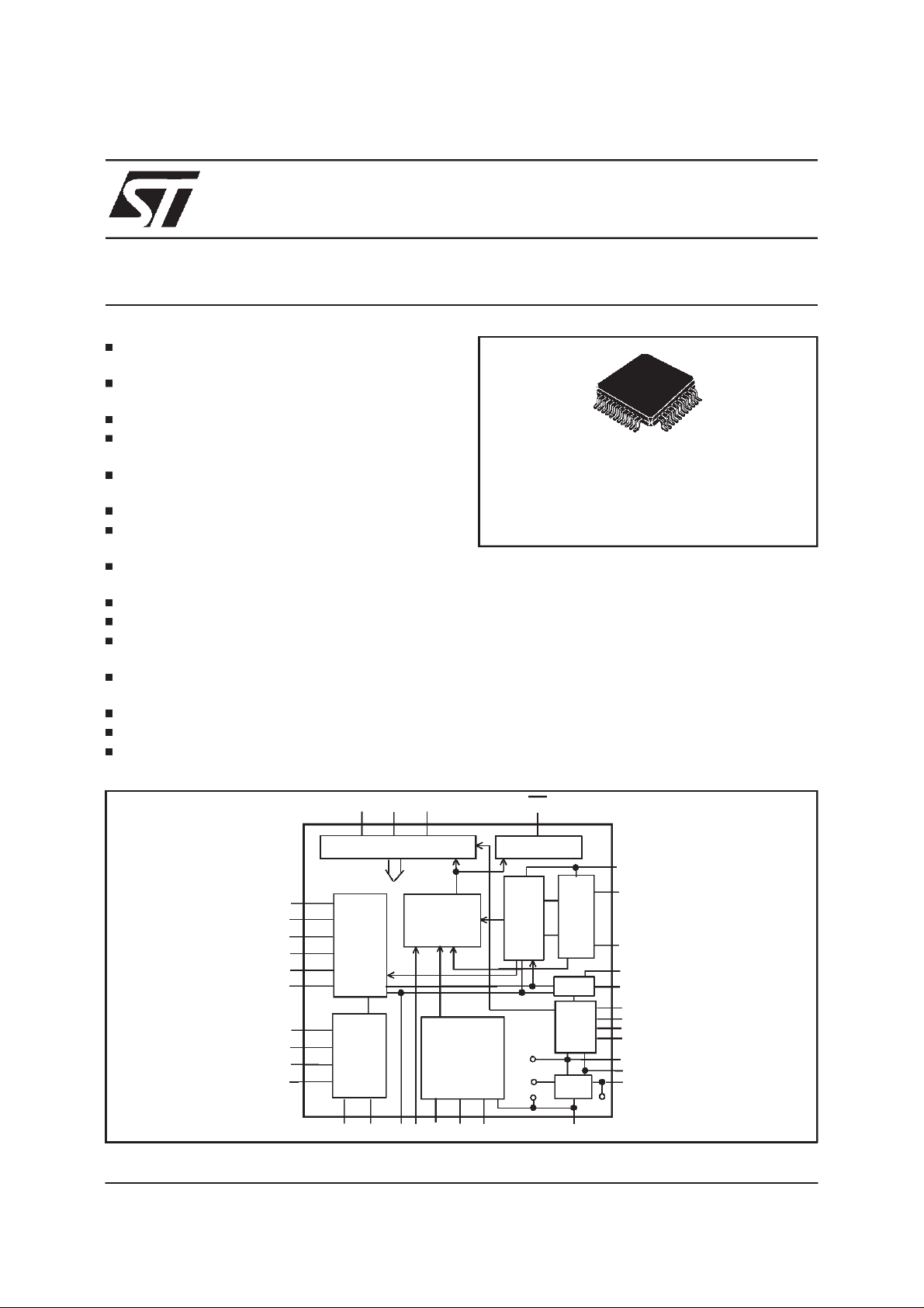
BLOCKDIAGRAM
ORDERING NUMBERS: STLC3055Q
DESCRIPTION
The STLC3055 is a SLIC device specifically designed for WLL (Wireless Local Loop) and ISDNTerminalAdaptors. One of the distinctive characteristic of this device is theability to operate with
a single supply voltage (from +5.5V to +15.8V)
and self generate the negative battery by means
of an on chip DC/DC converter controller that
drives an externalMOSswitch.
The battery level is properly adjusted depending
on the operatingmode. A useful characteristic for
TQFP44
STLC3055QTR
October 1999
TX
RX
ZAC1
ZAC
RS
ZB
CKTTX
CTTX1
CTTX2
FTTX
D0 D1 D2 DET
INPUT LOGICAND DECODER
Status and functions
SUPERVISION
AC PROC
TTX PROC
RTTX CAC ILTF RD IREF RLIM RTH
REFERENCE
OUTPUT LOGIC
LINE
DRIVER
Vcc
Vss
Agnd
OUTPUT
STAGE
DC PROC
DC/DC
CONV.
VOLT.
REG.
AGND
Vbat
BGND
TIP
RING
CREV
CSVR
CLK
RSENSE
GATE
VF
CVCC
VPOS
VBAT
1/22
STLC3055
DESCRIPTION (continued)
these applications is the integratedringing generator.
The control interface is a parallel type with open
drainoutput and3.3V logiclevels.
The metering pulses are generated on chip starting fromtwo logic signals(0, 3.3V) one define the
metering pulse frequency and the other the meteringpulse duration. An on chipcircuit then provides the proper shaping and filtering. Metering
pulse amplitude and shaping (rising and decay
time) can be programmed by external components. A dedicated cancellation circuit avoid pos-
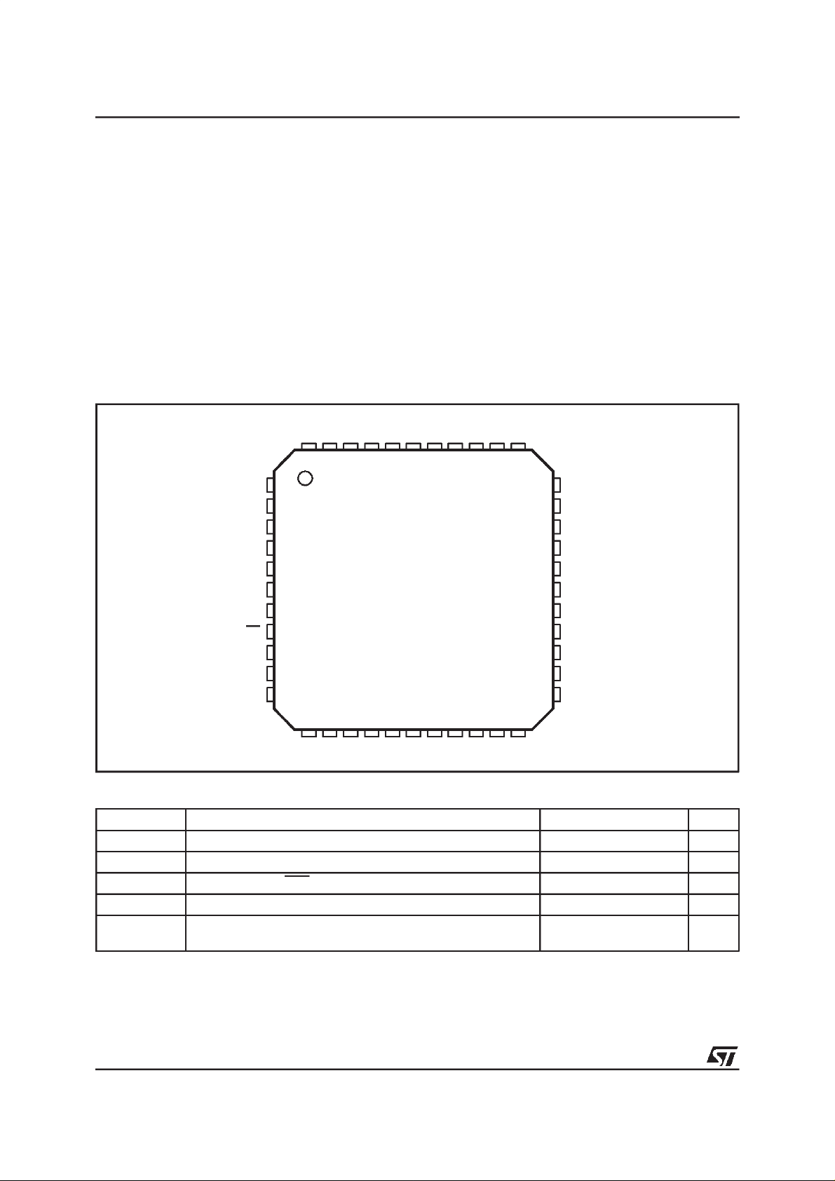
PIN CONNECTION
VBAT1
CREV
N.C.
TIP
44 43 42 41 3940 38 37 36 35 34
sible CODEC input saturation due to Metering
pulse echo.
Constant current feed can be set from 20mA to
40mA. Off-hook detection threshold is programmable from 5mAto 9mA.
The device, developed in BCD100II technology
(100V process), operates in the extended temperature range and integrates a thermal protection that sets the device in power down when Tj
exceeds140°C.
N.C.
N.C.
N.C.
RING
N.C.
VBAT
BGND
RES
N.C.
N.C.
DET
CKTTX
CTTX1
CTTX2
1
D0
2
D1
3
D2
4
PD
5
6
7
8
9
10
12 13 14 15 16
RX
FTTX
RTTX
171118 19 20 21 22
ZB
RS
ZAC
ZAC1
CAC
TX
VF
CLK
33
32
31
30
29
28
27
26
25
24
23
D97TL279A
CSVR
ILTF
RD
RTH
IREF
RLIM
AGND
CVCC
VPOS
RSENSE
GATE
ABSOLUTEMAXIMUM RATINGS
Symbol Parameter Value Unit
V
pos
A/BGND AGND to BGND -1 to +1 V
V
dig
T
j
(1)
V
btot
Positive Supply Voltage -0.4 to +17 V
Pin D0, D1, D2, DET, CKTTX -0.4 to 5.5 V
Max. junction Temperature 150 °C
Vbtot=|Vpos|+|Vbat|. (Totalvoltage applied tothe device
100 V
supply pins).
(1) Vbat is selfgenerated bythe on chip DC/DC converter and can be programmed via RF1 and RF2.
RF1and RF2 shall beselected in order tofulfil the a.mlimits (see External Components Table page 10)
2/22

STLC3055
OPERATINGRANGE
Symbol Parameter Value Unit
V
pos
A/BGND AGND to BGND -100 to +100 V
V
dig
T
op
(1)
V
bat
(1) Vbat is selfgenerated bythe on chip DC/DC converter and can be programmed via RF1 and RF2.
RF1and RF2 shall beselected in order tofulfil the a.mlimits (see External Components Table page 10)
THERMALDATA
Symbol Parameter Value Unit
R
thj-amb
PIN DESCRIPTION
N. Name Function
25 VPOS Positive supply inputranging from 5.5Vto 15.8V.
34 BGND Battery Ground, must beshorted with AGND.
27 AGND Analog Ground, must be shortedwith BGND.
16 ZAC AC impedance synthesis.
15 ZAC1 RX bufferoutput, the AC impedanceis connected fromthis node to ZAC.
17 RS Protection resistors image (theimage resistor is connectedfrom this node to ZAC).
18 ZB Balance Networkfor 2 to 4 wire conversion (the balanceimpedance ZB is connectedfrom this
20 TX 4 wire output port (TXoutput). The signal is referred toAGND. If connected to single supply
14 RX 4 wireinput port (RX input); 300KΩinput impedance. This signal is referred to AGND. If
19 CAC AC feedbackinput, AC/DC split capacitor (CAC).
32 ILTF Transversal line current image output.
41 TIP 2 wire port; TIP wire (Ia is the current sourced from this pin).
37 RING 2 wire port;RING wire (Ib is the current sunk into thispin).
28 RLIM Constant current feedprogramming pin (viaRLIM). RLIM should be connected close to this
30 RTH Off-hook threshold programming pin (via RTH).RTH should be connected close to this pin
29 IREF Internal bias current setting pin. RREF should be connected close to this pin and PCB layout
43 CREV Reverse polaritytransition time control.One proper capacitor connected between thispin and
31 RD DC feedback and ring trip input. RD should be connected closeto this pin and PCBlayout
Positive Supply Voltage 5.5 to +15.8 V
Pin D0, D1, D2, DET, CKTTX, PD -0.25 to 5.25 V
Ambient Operating Temperature Range -40 to +85 °C
Self Generated Battery Voltage -74 max. V
Thermal Resistance Junctionto Ambient Typ. 60 °C/W
node to AGND. ZA impedance is connected from this node to ZAC1).
CODEC input it must beDC decoupled with proper capacitor.
connected to single supply CODECoutput itmust beDC decoupledwith proper capacitor.
pin andPCB layout should avoid noise injection on this pin.
and PCB layout should avoid noise injectionon this pin.
should avoid noise injection on this pin.
AGND is setting the reverse polarity transitiontime. This is the same transitiontime used to
shape the”trapezoidal ringing” during ringing injection.
should avoid noise injection on this pin.
3/22
STLC3055
PIN DESCRIPTION (continued)
N. Name Function
4 PD Power Down input. Normally connected to CVCC (or to logic level high). Can beused to set
26 CVCC Internal positive voltage supplyfilter.
35 VBAT Regulated battery voltage self generated by the device via DC/DC converter. Must be shorted
23 GATE Driver for external Power MOS transistor.
21 VF Feedback inputfor DC/DC converter controller.
22 CLK Power Switch ControllerClock (typ. 125KHz). From version marked STLC3055 A5, this pin
24 RSENSE Voltage input for current sensing. RSENSE should beconnected close to this pin and VPOS
1 D0 Control Interface: input bit0.
2 D1 Control Interface: input bit1.
3 D2 Control interface: input bit 2.
8 DET Logic interface output of the supervision detector(active low).
33 CSVR Battery supply filter capacitor.
12 RTTX Metering pulse cancellation buffer output. TTX filter network should be connected to this point.
13 FTTX Metering pulse buffer input this signal is sent to the line andused to perform TTX filtering.
10 CTTX1 Metering burst shaping external capacitor.
11 CTTX2 Metering burst shaping external capacitor.
9 CKTTX Metering pulse clock input (12 KHz or 16KHz square wave).
44 VBAT1 Frame connection. Must be shorted to VBAT.
5 RES Reserved, must be connected toAGND.
6, 7,36,
38,39,
40,42
NC Not connected.
FUNCTIONALDESCRIPTION
The STLC3055 is a device specifically developed
for WLL and ISDN-TAapplications.
It is based on a SLIC core, on purpose optimised
for these applications, with the addition of a
DC/DC converter controller to fulfil the WLL and
ISDN-TAdesignrequirements.
The SLIC performs the standard feeding, signallingand transmissionfunctions.
It can be set in three different operating modes
via the D0, D1, D2 pins of the control logic interface (0 to 3.3V logic levels). The loop status is
carriedout onthe DET pin (activelow).
The DETpin is an opendrain output to alloweasy
interfacingwithboth 3.3Vand 5Vlogic levels.
The fourpossible SLIC’soperatingmodes are:
Power Down
TIP andRing terminals in open circuitsetting PD=0 and D0=D1=0.
to VBAT1.
can also be connected to CVCC or AGND. Whenthe CLK pin is connected toCVCC an
internal auto-oscillation is internally generatedand it is used instead of the external clock.
When the CLK pin is connected to AGND, theGATE output is disabled.
pin. The PCB layoutshould minimize the extra resistanceintroduced bythe copper tracks.
If notused should be left open.
HighImpedanceFeeding (HI-Z)
Active
Ringing
Table 1shows how to set the differentSLIC operatingmodes.
Table1. SLICoperatingmodes.
PD D0 D1 D2 Operating Mode
0 0 0 X Power Down
1 0 0 X H.I. Feeding(HI-Z)
1 0 1 0 Active NormalPolarity
1 0 1 1 Active ReversePolarity
1 1 1 0 Active TTX injection (N.P.)
1 1 1 1 Active TTX injection (R.P.)
1 1 0 0/1 Ring (D2 bit toggles @ fring)
4/22

STLC3055
The DC/DC converter controller is driving an external power MOS transistor (P-Channel) in order
to generate the negative battery voltage needed
for device operation.
The DC/DC converter controller is synchronised
withan externalCLK (125KHZtyp.).
From version marked STLC3055 A5, it can be
synchronisedto an internalclock generatedwhen
the pin CLK is connected to CVCC. One sensing
resistor in series to Vpos supply allows to fix the
maximumallowed input peakcurrent.This feature
is implemented in order to avoid overload on
Vpos supply in case of line transient (ex. ring trip
detection).
The typical value is obtained for a sensing resistor equal to 110mΩ that will guarantee an average current consumptionfrom Vpos < 700mA.
When in on-hook the self generated battery voltage is set to a predefinedvalue.
This value can be adjustedvia one externalresistor (RF1) and it is typical -50V. When RINGmode
is selectedthis valueis increasedto -70V typ.
Once the line goes in off-hook condition, the
DC/DC converter automatically adjust the generated battery voltage in order to feed the line with
a fixedDC current(programmablevia RLIM) optimising in this way the power dissipation.
This operating mode is normally selected when
the telephoneis in on-hook in order to monitorthe
line status keeping the power consumption at the
minimum.
The output voltage in on-hook condition is equal
totheself generatedbatteryvoltage(-50V typ).
When off-hook occurs the DET becomes active
(lowlogic level).
The off-hook threshold in HI-Z mode is the same
value asprogrammed inACTIVE mode.
The DC characteristic in HI-Z mode is just equal
to the self generated battery with 2x(1500W+Rp)
in series (see fig.1), where Rp is the externalprotectionresistance.
Figure1. DCCharacteristicin HI-Z Mode.
IL
Vbat
2x(R1+Rp)
Slope: 2x(R1+Rp)
(R1=1500ohm)
OPERATINGMODES
Power Down
DC CHARACTERISTIC& SUPERVISION
Whenthis modeis selected theSLIC is switched
off and the TIP and RING pins are in high impedance. Also the line detectorsare disabled thereforethe off-hookconditioncannot be detected.
This mode can be selected in emergency condition when it is necessary to cut any current deliveredto the line.
This mode is alsoforced by STLC3055 in case of
thermaloverload(Tj > 140°C).
In this case the device goes back to the previous
status as soon as the junction temperature decreaseunder the hysteresisthreshold.
AC CHARACTERISTICS
The 2W port is set in high impedance, the TX
output buffer is a low impedance output, no AC
transmissionis possible.
High Impedance Feeding (HI-Z)
DC CHARACTERISTIC& SUPERVISION
VL
Vbat (-50V)
AC CHARACTERISTICS
The AC impedance shown at the 2W port
(TIP/RING) is the same as the DC one. The
TIP/RINGAC impedance will be 2x(1500Ω+ Rp)
or highimpedance.
Active
DC CHARACTERISTICS & SUPERVISION
When this mode is selected the STLC3055 pro-
videsboth DC feedingandAC transmission.
The STLC3055 feedsthe line witha constantcur-
rent fixed by RLIM (20mA to 40mA range). The
on-hook voltage is typically 40V allowing on-hook
transmission;the selfgeneratedVbat is-50V typ.
If the loop resistance is very high and the line
current cannot reach the programmed constant
currentfeed value,the STLC3055 behaveslike a
40V voltage source with a series impedance
equal to the protection resistors 2xRp (typ.
2x41Ω) plus the internal resistance. Fig. 2 shows
thetypical DCcharacteristicin ACTIVE mode.
5/22

STLC3055
Figure2. DC characteristicin ACTIVE mode
IL
Ilim
(20 to
40mA)
2Rp
10V
VL
Vbat (-50V)
The line status (on/off hook) is monitored by the
SLIC’s supervision circuit. The off-hook threshold
can be programmed via the externalresistor R
TH
in the range from5mA to 9mA.
Independentlyon the programmed constant cur-
rent value, the TIP and RING buffers have a currentsource capabilitylimited to70mA typ.
Moreover the power available at Vbat is controlled by the DC/DC converter that limits the peak
current drawn from the Vpos supply. The maximum allowed current peak is set by the R
SENSE
resistorand it is typically900mApk.
POLARITYREVERSAL
The D2 bit controls the line polarity, the transition
betweenthe two polaritiesis performed in a ”soft”
way. This means that the TIP and RING wire exchange their polarities following a ramp transition
(see fig.3). The transition time is controlled by an
external capacitor CREV. This capacitor is also
setting the shape of the ringing trapezoidal waveform.
Whenthe control pins set battery reversal the line
polarity is reversed with a proper transition time
setvia an externalcapacitor(CREV).
Figure3. TIP/RING typical transitionfrom
Directto ReversePolarity
GND
TIP
4V typ.
40V typ
ON-HOOK
dV/dT set
by CREV
RING
AC CHARACTERISTICS
The SLIC provides the standard SLIC transmis-
sion functions:
Input impedance synthesis: can be real or
complex and is set by a scaled (x50) external
ZACimpedance.
Transmit and receive: The AC signal present
on the 2W port (TIP/RING)is transferredto the
TX outputwith a -6dBgain and from the RX input to the2W portwith a 0dBgain.
2 to 4 wire conversion: The balance impedance can be real or complex, the proper cancellation is obtained by means of two external
impedanceZA and ZB.
Once in Active mode (D1=1) the SLIC can operate in different states setting properly D0 and D2
controlbits (see also Table 2).
Table2. SLICstates in ACTIVEmode
D0 D1 D2 Operating Mode
0 1 0 Active Normal Polarity
0 1 1 Active Reverse Polarity
1 1 0 Active TTX injection (N.P.)
1 1 1 Active TTX injection (R.P.)
METERING PULSE INJECTION(TTX)
The metering pulses circuit consist of a burst
shaping generator that gives a square wave
shaped and a low pass filter to reduce the harmonic distortionof theoutput signal.
The metering pulse is obtained starting from two
logicsignals:
CKTTX: is a square wave at the TTX frequency (12 or 16KHz) and should be permanently applied to the CKTTX pin or at least for
all the duration of the TTX pulse (including rising and decayphases).
D0: enable the TTX generation circuit and definethe TTXpulse duration.
This two signals are then processed by a dedicated circuitry integrated on chip that generate
the metering pulse as an amplitude modulated
shaped squarewave (SQTTX)(see fig.4).
Both the amplitude and the envelope of the
squarewave (SQTTX) can be programmed by
means of external components. In particular the
amplitudeis set by the two resistorsRLV and the
6/22
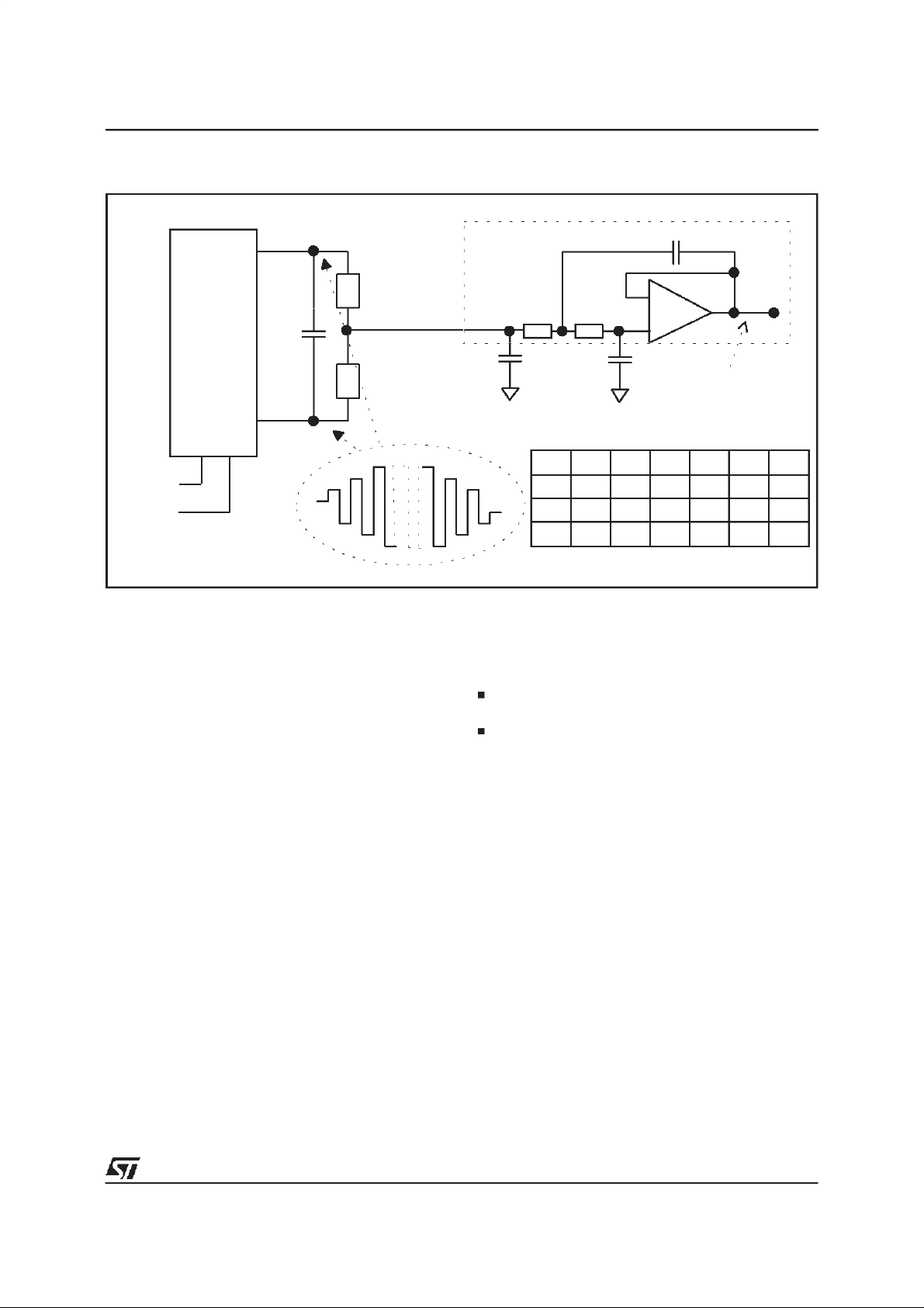
Figure4. Meteringpulse generationcircuit.
CTTX1
STLC3055
Low PassFilter
C1
RLV
BURST
SHAPING
GENERATOR
D0
CKTTX
Square wavepulse metering
CS
CTTX2
SQTTX
RLV
shapingby thecapacitorCS.
The waveform so generated is then filtered and
injectedon the line.
The lowpass filtercan be obtained usingthe inte-
grated buffer OP1 connected between pin FTTX
(OP1 non inverting input) and RTTX(OP1 output)
(see fig.4) and implementing a ”Sallen and Key”
configuration.
Dependingon the externalcomponents count it is
possible to build an optimised application depending on the distortion level required. In particular harmonic distortion levels equal to 13%,
6% and 3% can be obtained respectively with
first,second andthirdorder filters(see fig.4).
The circuit showed in the ”Applicationdiagram” is
relatedto thesimple firstorderfilter.
Once the shaped and filtered signal is obtained at
RTTX buffer outputit is injectedon the TIP/RING
pins with a +6dBgain.
It should be noted that this is the nominal condition obtained in presence of ideal TTX echo cancellation(obtained via proper settingof RTTXand
CTTX). In addition the effective level obtained on
the line will depend on the line impedance, the
protection resistor value and the series switch
(SW1or SW2)on resistance.
In the typical application (TTX line impedance
=200Ω ,RP=41Ω, SW1,2 on resistance = 9Ω
and ideal TTX echo cancellation) the metering
pulse level on the line will be 1.33 timesthe level
appliedto theRTTX pin.
RTTX
R1
CFL
R2
FTTX
OP1
+
C2
Sinusoidalwave
pulse metering
Required external components vs.filter order.
Order CFL R1 C! R2 C2 THD
1 X 13%
2 XXXX6%
3XXXXX3%
As already mentioned the metering pulse echo
cancellationis obtained by means of two external
components(RTTXand CTTX) thatshould match
the line impedance at the TTX frequency. This
simplenetwork has a doubleeffect:
Synthesise a low output impedance at the
TIP/RINGpins at theTTXfrequency.
Cut the eventual TTX echo that will be transferredfromthe line tothe TX output.
Ringing
When this mode is selected STLC3055 self generate an higher negativebattery (-70V typ.) in order to allow a balanced ringing signal of typically
65Vpeak.
In this condition both the DC and AC feedback
loop are disabled and the SLIC line drivers operateas voltagebuffers.
The ring waveform is obtained toggling the D2
controlbit atthedesired ringfrequency.This bitin
fact controls the line polarity (0=direct; 1=reverse). As in the ACTIVE mode the line voltage
transition is performed with a ramp transition,obtaining in this way a trapezoidal balanced ring
waveform(seefig.5).
The shaping is defined by the CREV external
capacitor.
Selecting the proper capacitor value it is possible
toget differentcrest factorvalues.
The following table shows the crest factor values
7/22
 Loading...