

SGS Thomson Microelectronics STLC1PD Datasheet

■ FULLY MONOLITHIC FIXED FREQUENCY
SMPS
■ THREE LOW SIDE DRIVERS FOR STOP
TAIL AND TURN LED LAMPS ARRAYS
DRIVING
■ PROGRAMMABLE LOW SIDE DRIVER
OVER CURRENT LIMIT PROTECTION
■ UNDER CURRENT DIAGNOSTIC
■ INPUT OVERVOLTAGE PROTECTION
■ VERY LOW STAND-BY CURRENT
■ THERMALPROTECTION WITH
HYSTERESIS
DESCRIPTION
The STLC1, a device realized with the well
established BCD technology, is a fixed f re quenc y
fully monolithic SMPS, with three independent
smart low side driver, p rima rily intended for
automotive rear led lamps driving.
STLC1
LED LAMPS CLUSTER DRIVER
PowerSO-20
The output voltage is set using a simple resistor
divider. Thermal shutdown with hysteresis, input
over-voltage and overcurrent protections give
robust des ign solutions.
TM
SCHEMATIC DIAGRAM
TURN
STOP
TAIL
CNTL
TS -PWM
GND
LMP -OU T
OSCILLATOR
PULSE WIDTH
CONTROLLER
OSC
LAMP
OUTAGE
DETECT
B+
THERMAL
PROTECTION
I
N
P
U
T
CONTOLLER
PWM
COMP
PWM
SWITCH
COMP1
M3
-
+
-
ERRAMP
+
REF
M2
ST - LTL-L
R
s
1.24V
TR -L
P-OUT
FDBK
REF
TR -DRV
M1
ST -DRV
TL - DRV
1/16September 2002
STLC1
ABSOLUTE MAXIMUM RATINGS
Symbol Parameter Value Unit
V
V
V
TURN,
V
STOP,
V
TAIL
I
TURN,
I
STOP,
I
TAIL
I
TR-DRV,
I
TL-DRV,
I
ST-DRV
I
LMP-OUT
V
P-OUT
I
P-OUT
T
T
Transient Supply Voltage (load dump)
B+
Operating Supply Voltage
B+
60 V
24 V
TURN, STOP and TAIL input pins voltage VB++ 0.3 V
TURN, STOP and TAIL pins current ± 10 mA
TR-DRV, TL-DRV and ST-DRV pins sink current 1.5 A
LMP-OUT pin sink current
P-OUT DC Voltage
P-OUT pin sink current
Storage Temperature Range
stg
Operating Junction Temperature Range
J
120 mA
60 V
Internally Limited A
-55 to +150 °C
-40 to +125 °C
THERMAL DATA
Symbol Parameter
R
thj-case
R
thj-amb
Thermal Resistance Junction-case
Thermal Resistance Junction-Ambient
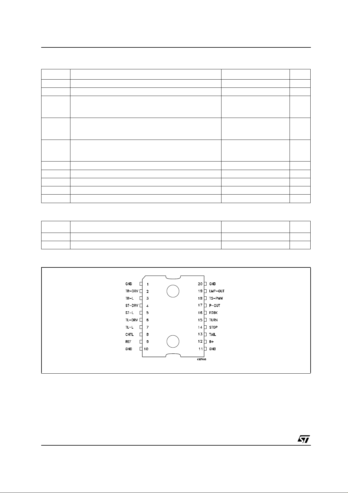
CONNECTION DIAGRAM (t op view)
PowerSO-20
TM
PowerSO-20
TM
2 °C/W
50 °C/W
Unit
2/16
PIN DESCRIPTION
Pin N° Symbol Name and Function
1 GND Ground
2 TR-DRV The Low Side Driver drain pin for the TURN LED array
3 TR-L The Low Side Driver source pin, used to detect either a lamp outage or an
over-current condition for the TURN LED array
4 ST-DRV The Low Side Driver drain pin for the STOP LED array
5 ST-L The Low Side Driver source pin, used to detect either a lamp outage or an
over-current condition for the STOP LED array
6 TL-DRV The Low Side Driver drain pin for the TAIL LED array
7 TL-L The Low Side Driver source pin, used to detect either a lamp outage or an
over-current condition for the TAIL LED array
8 CNTL Determines, according to a percentange of VREF,the Pulse Width Controller
internal oscillator duty cycle
9 REF Stable Reference Voltage
10 GND Ground
11 GND Ground
12 B+ Power Supply
13 TAIL TAIL input pin. When brought high, TAIL activates the IC anddrivestheTAIL led
array.
14 STOP STOP input pin. When brought high, STOP activates the IC and drives the
STOP led array.
15 TURN TURN input pin. When brought high, TURN activates the IC and drives the
TURN led array.
16 FDBK Internal Error Amplifier Inverting Pin
17 P-OUT Power MOSFET drain pin
18 TS-PWM A Three State Input. It determine the control logic for TAIL and STOP Low Side
Drivers.
19 LMP-OUT A weak pulled up signal during lamps No Fault condition and an active pulldown
when a Fault condition is detected.
20 GND Ground
STLC1
ORDERING INFORMATION
TYPE
STLC1 STLC1PD
PowerSO-20
TM
3/16
STLC1
TYPICAL APPLICATION CIRCUIT
TURNTAIL
STOP
RC1
RLR
RLS
RLT
RC2
Iout
OUT
C
OUT
RF1
GND
TR-DRV
TR-L
R
TR
ST-DRV
ST-L
R
TS
TL-DRV
TL-L
R
TT
CNTL
REF
C
GND
REF
GND
LMP-OUT
TS-PWM
P-OUT
FDBK
TURN
STOP
TAIL
GND
IP-OUT
B+
RF2
C
SEPIC
ELECTRICAL CHARACTERISTICS FORSMPD SECTION(T
Typical values are referred at T
=25°C, VB+=14V)
J
=-40 to125°C unless otherwise specified.
J
Symbol Parameter Test Conditions Min. Typ. Max. Unit
V
Supply Operating Voltage Normal Operating Range 9 24 V
B+
Normal Operating Range - TAIL only 6 24
V
I
SQ
f
osc
R
P(on)
I
D(off)
I
LIMITIP-OUT
t
SMPS-ON
V
LOAD
V
LINE
B+ Input Overvoltage
SD
Shutdown
Total Off State Quiescent
Current
VB+=14V, V
=0V
TURN=VSTOP=VTAIL
28 30 32 V
120 180 µA
PWM Oscillator Frequency VB+= 14V 140 180 240 kHz
Static drain to ground
SMPS N-channel switch
on resistance
P-OUT Off State leakage
=9V, I
V
B+
=14V, I
V
B+
=4A 180 mΩ
P-OUT
=4A 170 mΩ
P-OUT
VB+= 16V, 20 µA
Current
Current Limit VB+=14V, V
SMPS Turn On Delay C
=1µF (see note 1,4 and Fig 1, 2) 1.6 ms
REF
Load Regulation VB+=14V, I
V
=10V
OUT
Line Regulation VB+= 9 to 16V, I
V
=10V
OUT
= 1V 8 12 16 A
FDBK
= 0.6 to 3A
OUT
OUT
= 1.5A
60 mV
15 mV
4/16

STLC1
ELECTRICAL CHARACTERISTICS F OR LOW SIDE DRIVER SECTION (TJ=-40 to 125°C unless
otherwise specified. Typical v alues are referred at T
Symbol Parameter Test Conditions Min. Typ. Max. Unit
R
(on)
I
LSD(off)
t
LSD-ON
V
LS-ON
V
LS-OFF
f
LSD
V
IN(ON)
V
IN(OFF)
Static drain to source LSD
N-channel switch on
resistance
OFF State LSD’S leakage
current
LSD Turn On Delay C
FDBK Voltage over which
LSD’s are enabled
FDBK Voltage over which
LSD’s are disabled
Pulse Width Controller
Internal Oscillator
Frequency
Input Threshold voltage to
enable LSD
Input Threshold voltage to
disable LSD
VB+=9V, V
V
TURN=VSTOP=VTAIL
V
TR-DRV=VST-DRV=VTL-DRV=VB+
=1µFC
REF
(see note 2,4 and Fig 1, 2)
V
TAIL=VB+VTS-PWM=VREF
VB+= 9 to 16V
VB+= 9 to 16V
=25°C, VB+=14V)
J
TURN=VB+VTR-L
I
=1A
TR-DRV
V
STOP=VB+VST-L
I
=1A
ST-DRV
V
TAIL=VB+VTL-L
I
=1A
TL-DRV
=0V
= 220µF
OUT
=0V
=0V
=0V
500 mΩ
500 mΩ
500 mΩ
10 µA
2ms
0.95V
FB
0.5V
FB
/2 200 380 500 Hz
0.6V
B+
0.4V
B+
V
V
V
V
5/16
 Loading...