


■
Low power architecture -- Class AB, current
drive, output stage through a centre tapped
transformer to facilitate power supply switching
between 5.0V and a lower voltage. (3.3V in the
reference design) This gives a reduction in
power consumption.
■
480mW power consumption with a typical G.lite
signal.
■
600mA current driving capability
■
Positive +5.0V and one lower supply. (3.3V in
the reference design)
■
Switching power supplies to save power
■
Thermal overload shutdown
■
Four programmable receive gains
■
Opamp for a low pass filter in the receive path
■
Undedicated opamp with separate power down
control (used as a transmit path filter in the
reference design)
■
Separate power down control for Tx and Rx
path
■
48-pin TQFP (7x7x1.4mm) package
STLC1512
NorthenLite™ G.lite Loop Driver
PRODUCT PREVIEW
TQFP48 (7x7x1.40)
ORDERING NUM BER: STLC 1512
1.0 GENERAL DESCRIPTION
The STLC1512 G.lite line driver chip contai ns the l ine
driver as well as part of the receive path required i n a
central office G.lite modem. It provides an interface
between the AFE chip (STLC1511) and the telephone line. The line driver chip has been designed
with low power consumption, high signal to noise
plus distortion ratio and high current driving capability.
Figure 1. Block Diagram
DCFBON
PAIN
DCFBOP
AMPIN
TX REF
Buffer
RX REF
Buffer
LPF AMP
OPAMP
Thermal
Shutdown
BIAS
AMPIP
AMPOUT
PAI P
TXANG
RBIAS
REF2P5
RXANG
LPFIN
LPFOUT
November 2000
This is preliminary information on a new product now in development. Details are subject to change without notice.
Feedback
Preamp
PGA
DC
Amp
Power
Stage
DCFBIP
DCFBIN
FPP
PWRVEE x
PAOPx
BUFFP
BUFFN
FPN
PAON x
RXPD
AMPPD
TXPD
PGAIN
PGA1
PGA0
PGAOUT
1/26

STLC1512
1.0 GENERAL DESCRIPTION
The line driver transmit path contains a preamplifier
followed by a power output stage. The power stage
has current outputs that directly drive the primary
side of a center tapped transformer.
The receive path contains a programmable gain amplifier followed by an opamp which is used with off
chip passive components in an active low pass filter.
The Programmable Grain Amplifier (PGA) has four
steps optimized for the recommended G.lite CO line
interface.
There is also an undedicated opamp which can be
used for active filtering in either the transmit or re-
Figure 2. STLC1512 pinout
AMPIP
AMPIN
AMPOUT
TXVCC3
TXVCC2
DCFBON
ceive paths
2.0 PACKAGING AND PIN INFORMATION
2.1 Package Technology
STLC1512 will be packaged in a TQFP 48 package,
according to JEDEC Specification reference MS026-BBC.
2.2 STLC1512 Pin Allocation
The pin out for the STLC1512 is depicted in the following Figure 2.
TXVCC1
TXVEE1
TXVEE2
TXVEE3
QVEETX
DCFBIP
DCFBIN
NC
DCFBOP
TXANG
FPP
FPN
PAIP
PAIN
RBIAS
REF2P5
NC
LPFOUT
LPFIN
48
PWRVEE1
PWRVEE2
PAOP1
PAOP2
BUFFP
TQFP48 (7x7x1.4mm)
BUFFN
PAON1
PAON2
PWRVEE3
PWRVEE4
1
PGAIN
RXANG
RXVCC1
PGAOUT
RXVCC2
RXVEE1
QVEERX
PGA0
RXVEE2
PGA1
TXPD
AMPPD
RXPD
2/26
2.3 Pin Description
The pin description for the STLC1512 is given in the following Table 1.
Table 1. Pin Description
STLC1512
Pin # Pin Name Pin Type
1 PGAOUT AO Rx PGA output (programmable gain amplifier)
2 PGAIN AI Rx PGA input
3 RXANG AO 2.5V Rx buffered reference
4 RXVCC1 VCC +5.0V supply for Rx path circuitry
5 RXVCC2 VCC +5.0V supply for Rx path circuitry
6 QVEERX VEE Quiet ground for the Rx circuitry
7 RXVEE1 VEE Ground for Rx path circuitry
8 RXVEE2 VEE Ground for Rx path circuitry
9 PGA0 DI PGA gain setting control bit 0
10 PGA1 DI PGA gain setting control bit 1
11 TXPD DI Tx path power down control (Active low)
12
13 RXPD DI Rx path power down control (Active low)
14 PWRVEE4 VEE Power stage ground.
15 PWRVEE3 VEE Power stage ground.
16 PAON2 AO Tx Power Amplifier Negative output
AMPPD
2
DI Undedicated opamp power down control (Active low)
Pin Description
1
17 PAON1 AO Tx Power Amplifier Negative output
18 BUFFN AO Current generator buffer negative output
19 BUFFP AO Current generator buffer positive output
20 PAOP2 AO Tx Power Amplifier Positive output
21 PAOP1 AO Tx Power Amplifier Positive output
22 PWRVEE2 VEE Power stage ground.
23 PWRVEE1 VEE Power stage ground.
24 NC Not connected
25 DCFBIN AI Power amp DC feedback amplifier negative input
26 DCFBIP AI Power amp DC feedback amplifier positive input
27 QVEETX VEE Quiet ground for Tx circuitry
28 TXVEE3 VEE Ground for Tx path circuitry
29 TXVEE2 VEE Ground for Tx path circuitry
30 TXVEE1 VEE Ground for Tx path circuitry
31 TXVCC1 VCC +5.0V supply for power amp output stage
3/26
STLC1512
Table 1. Pin Description
32 TXVCC2 VCC +5.0V supply for power amp output stage
33 TXVCC3 VCC +5.0V supply for Tx path circuitry and bias blocks
34 AMPOUT AO Undedicated opamp output
35 AMPIN AI Undedicated opamp negative input
36 AMPIP AI Undedicated opamp positive input
37 DCFBON AO Power amp DC feedback amplifier negative output
38 DCFBOP AO Power amp DC feedback amplifier positive output
39 TXANG AO 2.5V Tx buffered reference
40 FPP AO Fast path positive output
41 FPN AO Fast path negative output
42 PAIP AI Tx Power amplifier positive input
43 PAIN AI Tx Power amplifier negative input
44 RBIAS AO Reference resistor generating bias current
45 REF2P5 AI Externally supplied 2.5V reference
46 NC Not connected
47 LPFOUT AO LPF (low pass filter) Op Amp output
48 LPFIN AI LPF (low pass filter) Op Amp negative input
<1>The values of the components that are conne ct ed to the pins a re shown in Figure 11.
<2>If the undedicated opamp is used in the transmit path, AMPPD can be connected to TXPD on the board. If the undedicated opamp
is used in t he receive pat h, AMPPD can be connected to RXPD on the board. This opamp is powered of f of TXVCC3.
3.0 FUNCTIONAL DESCRIPTION
The STLC1512 consists of the following functional
blocks:
■
Transmit Signal Path
■
Receive Signal Path
■
Thermal Protection
The transmit signal that comes from the AFE is filtered before it reaches the line driver. STLC1512
contains an opamp that can be utilized as part of this
filter. The AMPPD pin allows this op amp to be powered down independently. The line driver consists of
a preamp followed by a current drive power stage.
The preamplifier provides large open loop gain while
the power stage provides open collec tor current drive
to allow for single supply sw itchi ng. The center tap of
the primary side of the transformer is connected to a
supply that can be switched between 5.0V and a lower supply to realize power savings on a DMT signal.
The reference design sets this supply at 3.3V. The
line driver can be powered down by a low at the
TXPD pin.
The receive path consists of a Programmable Gain
Amplifier (PGA) and an active low pass filter. The
PGA is programmable in four steps. The active low
pass filter is composed of an on chip op amp and external passive components. The receive signa l passes through the PGA, is low pass filtered and then
driven off chip to the AFE chip. Both the PGA and the
opamp can be powered down by RXPD signal.
A thermal protection circuit has als o been implemented on the chip to prevent the chip from overheating
under fault conditions.
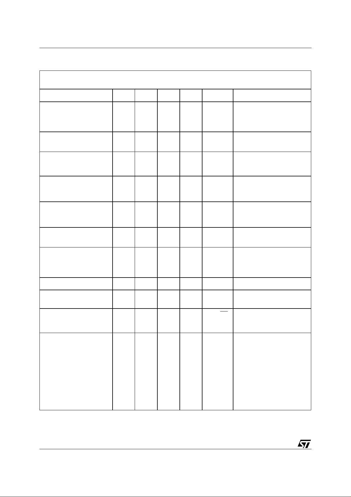
4.0 SPECIFICATIONS
4.1 Chip Specifications
The cross-talk specifications are based on the assumption that cross-talk should not degrade the
SNDR of the receive signal. If there is receive crosstalk into the transmit path, this signal will come back
through the hybrid balance and cause noi se in the receive path. If the signal is undistorted it will cause a
small gain and phase error which will not affect performance. If it is distorted it will cause an increased
4/26
STLC1512
noise floor which will degrade the SNDR of the receive signal.
The same is true of the transmit signal. If the signal is
undistorted it will show up out of band in the receive
path and will not degrade SNDR. However, if the
Table 2. Chip Performance Specifications
Description min nom max Units Comments
Rx Cross-Talk into Tx
Undistorted
Rx Cross-Talk into Tx
Distorted
Tx Cross-talk into Rx
Undistorted
Tx Cross-talk into Rx
Distorted
-55 dB Measured from the active low pass filter
-73 dB Measured from the active low pass filter
-50 dB Measured from tip and ring to the active
-86 dB Measured from tip and ring to the active
4.2 Pow er A mpl ifi e r P erf or m a nce
Specifications
The power amplifier must be specified with all of the
external components in the application diagram.
Without these components the ampli fier wi ll not function correctly. S pecifications th at are measured at the
chip are specified as such in the comments.
transmit signal is distorted by the cross-talk mechanism it will show up in the receive band and could reduce the SNDR.
The cross-talk numbers are specified from output to
output under maximum gain conditions.
output in the receive path to tip and ring.
output in the receive path to tip and ring.
low pass filter output with the maximum
gain setting in place.
low pass filter output with the maximum
gain setting in place.
Table 3 contains the conditions over which the specifications in Table 4 apply . The limits on the speci fications in Table are valid over all of the ranges
specified in Table 3. The nominal values of the specification occur at the nom inal v alue of all of the conditions in Table 3 unless otherwise specified.
...
Table 3. Power A m pl i fier P erf ormance Limi t s
Description min nom max Units
Gain 19.9 20.1 20.3 dB
Ambient Temperature -40 27 85
Line Impedance 80 100 160 W A nominal chip will have no problem
Supply voltage for TXVCC 4.75 5.0 5.25 V
<1>Nomi nal specifica tions are for n om i nal bias and pr ocess
<2>Maxim um and minimum specificat i ons are for worst case proc ess and bias co nditions
o
C
driving 200 Ω or 50 Ω.
Comments
1,2
5/26
STLC1512
Table 4. Power Amplifier Performance Specifications
Unless otherwise specified nom specs apply to the nom conditions in attribute and the max and min conditions are
defined by the process and other spec limits that give these worst case corners.
Description min nom max Goal Units Comments
Quiescent current at PAOP/
1
PAON
Total quiescent current at
output stage
Input bias current
2
3
Minimum Voltage at PAOP/
4
PAON
High Current Drive
Minimum Voltage at PAOP/
5
PAON
Low Current Drive
Common mode input
voltage range
6
Peak output sink
current on pin PAOP and
7
PAON
10 15 18 mA The spec is measured as the
sum of the currents at
POAP1+PAOP2 or
PAON1+PAON2.
20 30 36 mA Measured at the center tap of
the transformer.
15 µA Measured at pin PAIP/PAIN.
This parameter cannot be
measured very accurately.
0.85 Vpeak Measured at pin PAOP1,2/
PAON1,2
0.70 Vpeak Measured at pin PAOP1,2/
PAON1,2
1.6 VCC-
V Measured at pin PAIP/PAIN
0.5
600 1000 mA This is the sum of the current
from PAOP1 and PAOP2 or
the sum of the currents from
PAON1 and PAON2
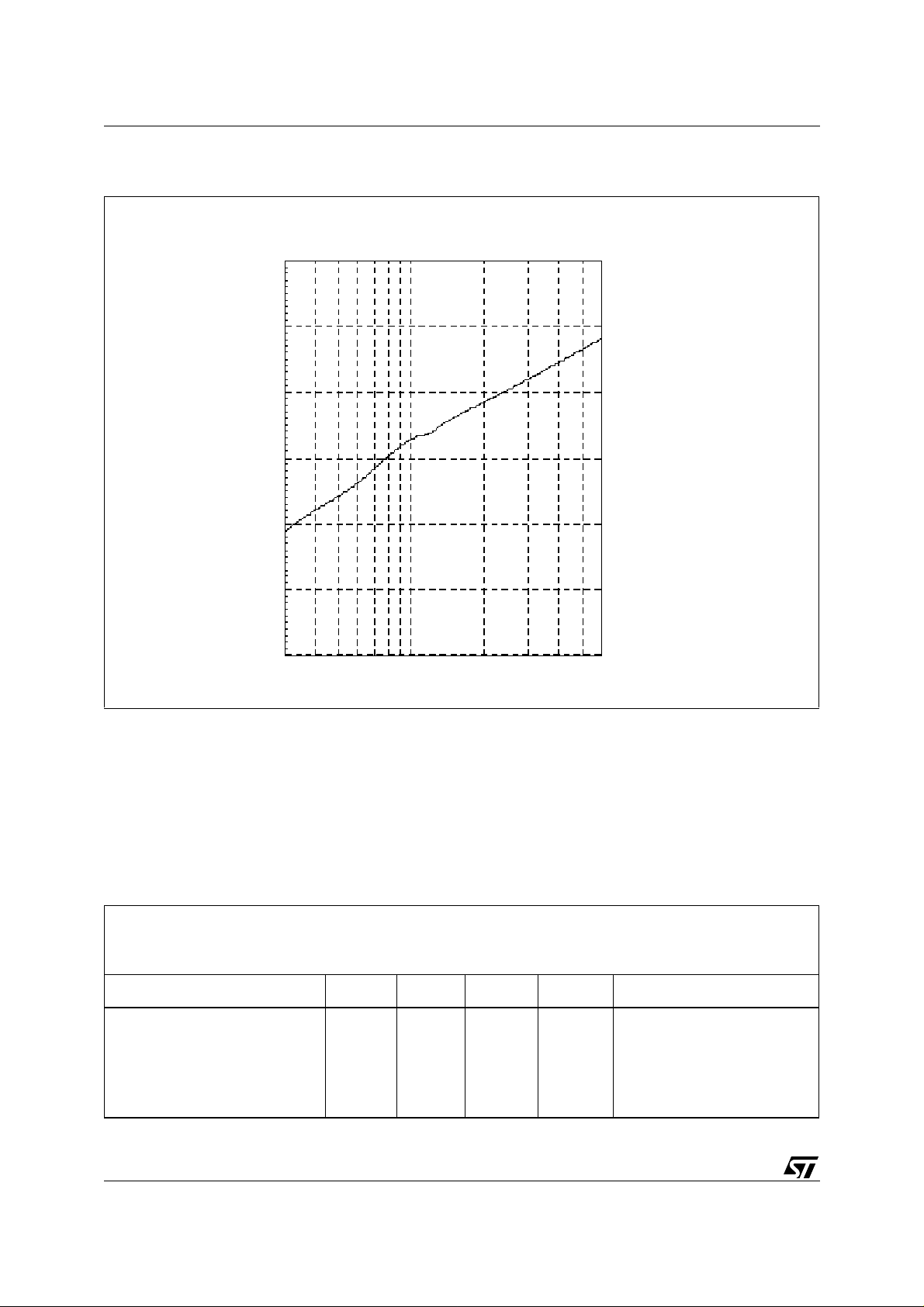
Power supply rejection See Figure 3.
Slew Rate
8
Output referred noise
9
voltage
Signal to distortion ratio
Two tone A
10
Im2 @ 200 kHz
Im3 @ 100 kHz
Two tone B<Superscript>10
Im3 @ 550 kHz
Output DS Multi-tone
11
28kHz < f < 121kHz
151kHz < f < 541kHz
35 V/µS Measured across the 100
Ohm line impedance
78 120 nV/÷√Hz measured at f=120kHz
Simulated to be good from
30kHz to 540kHz.
Measured at the line
impedance. The 4 to 1
78
78
86
86
dB
dB
transformer must have total
harmonic distortion better
than 50dB over 30kHz < f <
59
59
dB
550kHz.
The multi-tone spec is the
78
59
85
66
86
59
dB
dB
important spec. The two tone
specs exist because the test
equipment may not be able to
create a good enough multitone input signal.
6/26

Table 4. Power Amplifier Performance Specifications
STLC1512
e
------------------------- -log=
n
2
100
o
C
x 1000
Only the power amplifier is
shut down under overheat
condition
Thermal shutdown junction
temperature
<1> The quiescent current is th e current flo wi ng into pin PAOP/PAON when there is no signal.
<2> This is the cu rrent drawn from the power supply that is connected to the center tap on the primary side of the transforme r.
<3> This is the cu rrent flowing into the pin PAIN or PAI P when there is no signal. The nature of the test set up m akes this qua n tity
<4> This will allow the distortion specs to be met while driving a 160W line impedance. This applies for a 550mA output current. The
<5> This spec is meant as an aid in calculating the proper switching poi nt. It appli es for a 225mA ou tput current.
<6> This is a requirement on the input signal that allows the distortion spec to be met. It is not a testable parameter. The range has
<7> The minim um sink current refers to peak signal current in normal operation. This is tested by placing a 80 W lo ad as th e l i n e
<8> Slew Rate spec is to guarantee that there is no slewing limit on a ma xi m um amplitude sine wave at 540kHz. A 100 mV ste p is
<9> Measured ac ross the 100 Ohm l i ne impedanc e. This noise spec can be converted to dB/Hz through the followin g formula,
<10> Two tone dis torti on is measur ed w ith tw o sin e wave s wi th eac h sine wa ve at an amp litu de of 1/2 f ull scal e (fo r sig nal g ain of
<11> A multi-tone sine wave is used for the DS (Down Stream) Multi-tone test. (The multi-tone signal will be 91 sine waves equally
<12> The thermal shut down can not be directly tested in pr oduction. It will b e investigated at bench and a correlation will be done
12
very difficult to measure. It is verified through simulation.
worst case impedance f or a nominal chi p i s 200 W.
been arrive d at from simu l ations.
impedance and ensuring that the amplifier still passes the distortion tests. The maximum sink current refers to the current that
will be delivered if tip and ring are shorted. A nominal chip can drive a 50W load while a worst case chip will drive 80W.
placed at the power amp input and the slew rate at the output of the amplifier is measured across the 100 Ohm load impedance.
The effect of the noise in the receive path can be obtained by subtracting the hybrid balance number.
20.1dB, the full scale signal at power amplifier input is 1.05 Vp). The two tone distortion requirement is measured from the rms
voltage of a single signal tone to the rms voltage of the distortion product. For the Two Tone A spec the tones are at f1=500KHz
and f2=300KH z gi ving Im2=20 0kHz and Im3=100 kHz. For the Two tone B the to nes are at f1= 500kHz and f2=450kHz so that
Im3=550kHz.
spaced from 35x4.3125kHz to 125x4.3125kHz with a peak-to-rms voltage ratio of 5.3 and an rms voltage equal to 208mV. Each
tone will have a peak amplitude of 30.8mV) The multi-tone test measures the difference between the power of the test tones
and the maximum power of a s i ngl e distortion product in the given bands .
hermal shut down temperature.
130 150 175
N
dB
10
7/26
STLC1512
)
Figure 3. Powe r Su ppl y Re j ect io n of t he P ower Amplifie r
WDB (PAOUT
-40
-60
dB
-80
1
-100
3.00e+04 1 .00e+ 05
6.00e+05
Hz
<1>This is a nominal specification. 6 dB of margi n should be added to arrive at a worst case spec.
4.3 Programmable Gain Ampl ifier (PGA) Performanc e Specification s
It should be noted that the PGA and LPF in the receive path must be AC coupled to avoid problems with amplifying any offsets.
Both the PGA and the amplifiers are specified in terms of the silicon only. This is to allow the system design to
be more flexible. The appendices show how to convert some of the silicon specs to system specs.
Table 5. PGA performance Specifications
Unless otherwise specified, NOM specifications apply for VCC=5.0V, temperature range outlined in Table 4.4,
nominal process and bias current. MAX and MIN performances with 5% variation on VCC, -40 <= T
and worst case process and bias current and a minimum load of 440 W.
DESCRIPTION MIN NOM MAX UNITS COMMENTS
Absolute Voltage Gain
D=00
D=01
D=10
D=11
1,2
11.4
1.4
-5.6
-19.8
11.8
1.8
-5.2
-19.2
12.2
2.2
-4.8
-18.8
dB
dB
dB
dB
Where ‘D’ is the binary value
of the control word
[PGA1, PGA0]
Gain settings are from the pin
PGAIN to pin PGAOUT (See
‘application diagram’)
ambient
<=85oC,
8/26