

■
Wide transmit (~80dB) and receive (~69dB)
dynamic range to limit the external filtering
requirements for extended loop reach operation
■
Programmable tx gain: 0 ÷ -32dB in 2dB steps
■
14-bit D/A converter in transmit path
■
Programmable rx gain: 0 ÷40dB in 0.5dB steps
■
12-bit A/D converter in receive path
■
Integrated phase-locked loop with an externall
LC or crystal oscillator
■
Low power: 300mW @ 5.0V
■
64-pin TQFP package
1.0 GENERAL DESCRIPTION
The STLC1511 G.lite Analog Front End (AFE) chip
implements the analog transceiver functions required
in both a central office modem and a customer
premise modem. It connects the digital modem chip
with the loop driver and hybrid balance circuits. The
STLC1511 has been designed with excellent dynamic range in order to greatly reduce the external filtering requirements at the front end. The AFE chip and
its companion digi tal chip along with a loop driv er, implement the complete G.992.2 DMT modem solution.
STLC1511
NorthenLi te™ G.lite BiCM OS
Analog Front-End Circuit
PRODUCT PREVIEW
TQFP64
ORDERING NUM BER: STLC 1511
The STLC1511 transmit path consists of a 14-bit
Nyquist rate D/A converter, followed by a programmable gain amplifier (TxPGA). The transmit gain is
programmable from 0 to -32dB in 2dB steps.
The STLC1511 receive path contains a buffer amplifier followed by a programmable gain amplifier (RxPGA), a low pass anti-aliasing filter, and a 12-bit
Nyquist rate A/D converter. The RxPGA is digitally
programmable from 0 to 40dB in 0.5dB steps.
2.0 PACKAGING AND PIN INFORMATION
2.1 STLC1511 Pin Allocation
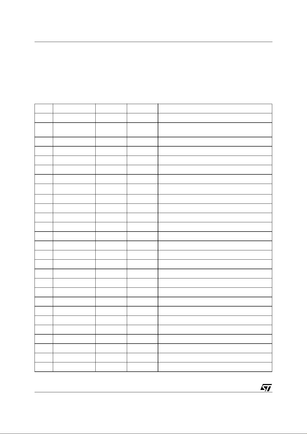
The pinout for the STLC1511 is depicted in Figure 1.
Figure 1. STLC1511 pinout
QVEEDAC
TXDADC1
VEEDAC
VCCDAC
VDDESD2
VSSESD2
VEETXPGA
VCCTXPGA
TXON
TXOP
RXOPINP
VCCRXPGA
QVEETX
48
47
46
45
44
43
42
41
40
39
38
37
36
35
34
33
TQFP64
QVEERX
VEERXPGA
QVEEBIAS
VEEBIAS
VCCBIAS
IREF50m
V3P75V
VCCPLL
VEEPLL
FREQ
OSCNE
OSCNB
OSCPB
OSCPE
VCAP
VDDPLL
VSSPLL
QVEEPLL
RESETN
TXSIN[0]
TXSIN[1]
FRMCLK
VSSDIG1
60
61
62
63
VDDDIG1
CK35M
DIGREF
RXSOUT[0]
RXSOUT[1]
VSSDIGE1
VSSDIG2
VDDDIGE1
VDDDIG2
DTX
DIGCLK
ENB
DRX
VEEADC
VCCADC
QVEEADC
64
1
2
3
4
5
6
7
8
9
10
12
13
14
15
16
17 18 19 20 21
ADCDC3
ADCDC2
59 58 57 56 5455 53 52 51 50 49
22 23 24 25 26
ADCDC1
VSSESD1
RXDCINP
VDDESD1
RXDCON
RXDCINN
RXINN
RXDCOP
271128 29 30 31 32
RXINP
RXOPIINN
November 2000
This is preliminary information on a new product now in development. Details are subject to change without notice.
1/31
STLC1511
2.2 Pin Description
Table 1. details the pinout assignment for the
STLC1511. The following list gives the different pin
types for the STLC1511.
■
VDD/VCC - 5V power supply
■
VEE/VSS - Ground supply
■
DO/DI - Digital Output/ Digital Input
■
AO/AI/AIO - Analog Output/ Analog Input/
Analog Input-Output
Table 1. Pin Assignement
Pin # Pin Name Pin Type Pad Type Description
1 VDDDIG1 VDD VDDCO 5V supply (digital) for ADC and DAC
2 CK35M DI TLCHT 35.328MHz serial interface clock input (also used in
Test Mode to test PFD. See Table on page 21)
3 DIGREF DO BT4CR 35.328/17.644MHz reference for Digital ASIC PLL
4 RXSOUT[0] DO BT4CR Rx serial data (lsb) output
5 RXSOUT[1] DO BT4CR Rx serial data (msb) output
6 VSSDIGE1 VSS VSSE Ground for digital output drivers
7 VSSDIG2 VSS VSSCO Ground supply for digital interface, serial interface
8 VDDDIGE1 VDD VDDE
9 VDDDIG2 VDD VDDCO 5 V supply for digital interface, serial interface
5 V supply for digital output drivers
1
10 DTX DO BT4CR Data Output for digital interface
11 DIGCLK DI TLCHT 35.328MHz clock input for digital interface
12 ENB DI TLCHT Enable input for digital interface
13 DRX DI TLCHT Data Input for digital interface
14 VEEADC VEE VSSCO Ground for ADC
15 VCCADC VCC VDDCO 5 V supply for ADC
16 QVEEADC VEE VSSCO Quiet ground for ADC circuitry
17 ADCDC3 AIO ANA ADC reference decoupling (3.75 V) 0.1uF
18 ADCDC2 AIO ANA ADC reference decoupling (2.5 V) 0.1uF
19 ADCDC1 AIO ANA ADC reference decoupling (1.25 V) 0.1uF
20 VSSESD1 VSS VSSA Ground for ESD ring
21 VDDESD1 VDD VDDA 5 V supply for ESD ring
22 RXDCINP AI ANA RxPGA positive input from DC blocking capacitor
23 RXDCINN AI ANA RxPGA negative input from DC blocking capacitor
24 RXDCON AO ANA RxPGA negative output to DC blocking capacitor
25 RXDCOP AO ANA RxPGA positive output to DC blocking capacitor
26 RXINN AI ANA Rx negative input (AC coupled)
27 RXINP AI ANA Rx positive input (AC coupled)
2/31
STLC1511
Table 1. Pin Assignement
Pin # Pin Name Pin Type Pad Type Description
28 RXOPINN AI ANA Rx opamp negative input (must be DC coupled)
29 RXOPINP AI ANA Rx opamp positive input (must be DC coupled)
30 VCCRXPGA VCC VDDCO 5V supply for RxPGA
31 VEERXPGA VEE VSSCO Ground for RxPGA
32 QVEERX VEE VSSCO Quiet ground for Rx circuitry
33 QVEEPLL VEE VSSCO Quiet ground for PLL circuitry
34 VSSPLL VSS VSSCO
35 VDDPLL VDD VDDCO
Ground for Oscillator
5 V supply for Oscillator
2
2
36 VCAP AO ANA Charge pump output to varactor
37 OSCPE AIO ANA Oscillator I/O (emitter)
38 OSCPB AIO ANA Oscillator I/O (base)
39 OSCNB AIO ANA Oscillator I/O (base)
40 OSCNE AIO ANA Oscillator I/O (emitter)
41 FREF AI ANA 2.56 MHz PLL input reference/ 35.328 MHz clock
input
42 VEEPLL VEE VSSCO
43 VCCPLL VCC VDDCO
Ground for oscillator
5 V supply for oscillator
2
2
44 V3P75V AIO ANA 3.75V output from Bandgap to 0.22mF capacitor
45
IREF50
m AIO ANA External resistor for bias current R=2.5V/
50mA=50kohm
46 VCCBIAS VCC VDDCO 5V supply for biasing
47 VEEBIAS VEE VSSCO Ground for biasing
48 QVEEBIAS VEE VSSCO Quiet ground for bias circuitry
49 QVEETX VEE VSSCO Quiet ground for Tx circuitry
50 TXOP AO ANA Tx positive output
51 TXON AO ANA Tx negative output
52 VCCTXPGA VCC VDDCO 5V supply for TxPGA
53 VEETXPGA VEE VSSCO Ground for TxPGA
54 VDDESD2 VDD VDDA 5V supply for ESD ring
55 VSSESD2 VSS VSSA Ground for ESD ring
56 VCCDAC VCC VDDCO 5V supply for DAC
57 VEEDAC VEE VSSCO Ground for DAC
58 TXDADC1 AIO ANA DAC reference (2.5V) 0.1uF
3/31
STLC1511
Table 1. Pin Assignement
Pin # Pin Name Pin Type Pad Type Description
59 QVEEDAC VEE VSSCO Quiet ground for DAC circuitry
60 RESETN DI TLCHT ResetN for the AFE
61 TXSIN[0] DI TLCHT Tx serial data (lsb) input
62 TXSIN[1] DI TLCHT Tx serial data (msb) input
63 FRMCLK DO BT4CR Tx 4.416MHz frame clock reference output
64 VSSDIG1 VSS VSSCO Ground (digital) for ADC and DAC
<1>H CMOS5 guidelines are fo r 1 pair of power/g r ound for 4 output dr i vers (4 m A)
<2>Pins 35 and 43 are both connected to the analog VCC supplying the on chip oscillator. Similarly, Pins 34 and 42 are connected
to analog VSS for th e oscillato r . Su pply lin e indu ctan ce is re duced u sing two p ads fo r VCC (an d VSS) in this manner. At the board
level, Pins 35 and 43 should be connected to analog VCC, and pins 34 and 42 should be connected to analog VSS.
3.0 FUNCTIONAL DESCRIPTION
3.1 General Functional Desc ription
The STLC1511 consists of the following functional
blocks:
■
Transmit Signal Path
■
Receive Signal Path
■
Phase Lock Loop and Amplifier for an external
oscillator .
■
Bias Voltage and Current Generation
■
Digital Interface
■
Serial Interface
The transmit path contains the 14-bit digital to analog
converter (DAC) necessary to generate the transmit
signal from a 14-bit digital input word. This transmit
signal is then scaled by the on chip programmable
gain amplifier (TxPGA) from 0 to -32dB in 2dB steps.
The scaled output signal is then driven off chip to the
external filters and power amplifier (PA) which drives
the DMT signal to the subscriber loop. The transmit
path is fully differential but may be used single ended
if both outputs from the TxPGA are terminated correctly.
The receive path c ontains an optio nal uni ty gain buffer followed by a two stage programmable gain amplifier (RxPGA), a 1st order low pass anti-aliasing filter,
and a 12-bit analog to digital converter (ADC). The
RxPGA consists of two s tages and the gain i s digitall y
programmable from 0 to 40dB in 0.5dB ste ps. The receive path is fully differential but may be used single
ended provided the other input to the RxPGA is
grounded.
The STLC1511 contains the circuits required to con-
struct a PLL that generates either a 17.644MHz/
35.328 MHz clock from a 2.56 MHz reference clock
when supplied with an external LC or crystal oscillator and tuning circuit. This clock is supplied to the
both the transmit and receive converters, and the serial interface used to transfer the Rx/Tx da ta betw een
the STLC1511 and digital chip. The STLC1511 also
has the ability to be driven directly by an external
35.328MHz clock supplied to the FREF pin.
The bias circuitry contains a bandgap voltage refer-
ence from which the converter references and analog
ground voltage is generated. This block also generates an accurate current using an external resistor
from which all of the S TLC1511 circuits are biased. In
addition, the bias circuitry also generates a 2.5V reference for the external Vco/Vcxo components and
can be used for other external circuits if necessary.
There is a 4 pin serial digital interface (
DIGCLK, ENB
) that loads a one of four 8-bit control
DTX, DR X,
register that controls all the programmable features
on the STLC1511. Refer to “Digital Interface And
Memory Map” on page 20 for more information on
the programmability of the AFE.
To facilitate data transfer between the STLC1511
and the digital ASIC (STLC1510), a 2-bit wide serial
interface for the transmit path and a 2-bit wide serial
interface for the receive path is incorporated into the
AFE. This in terface c onsists of tw o trans mit pins (
SIN[0:1]
), two receive pins (
necessary control signals (
RXSOUT[1:0]
FRMCLK, CK35M
TX-
), and the
) to
transmit the required data. For more information See
“Serial Interface” on page 18.
4/31
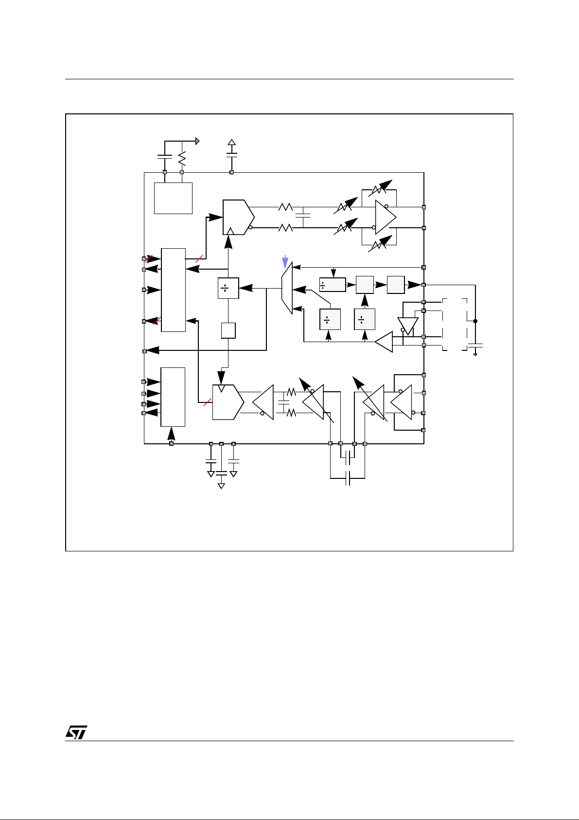
Figure 2. The block diagram of the STLC1511
50k
0.22uF
V3P5V
IREF50U
0.1uF
TXDADC 1
STLC1511
TX SIN[1:0]
FRM CLK
CK35M
RXS OU T[1:0]
DIGREF
DIGCLK
ENB
DRX
DTX
Band gap/
Bias Gen
2
2
Serial I/F
D igital I/F
RESETN
fp=2M H z
14-bit
DAC
14
4.416M
8/4
35.328M/
17.622M
I/F
dig
2.56M/35.328M
2/3/4/8
PFD
CP
TXON
TXOP
2.56M
(Os c il la t or M od e )
FREF
35.328M
(External Clock Mode)
VCAP
OSCNB
rn
e
t
Ex
Resonator
al
90
OSCPB
5
°
69
G
OSCPE
OSCNE
4.416M
12-bit
ADC
+
-
12
G=1
-
+
+
-
-+
fp=2 M Hz
0.1uF
0.1uF
0.1uF
ADCDC2
ADCDC1
ADCDC3
0.1uF
RXDCOP
RXDCIP
RXDCIN
RXDCO N
0.1uF
+
-
RXINN
RXOPINP
RXOPINN
RXINP
Shaded blocks are only usabe when the PLL is active. Crystal based external resonator for the CPE Mode, LC
based resonator for the CO Oscillator Mode. 35.328 MHz external reference in CO External Clock Mode.
3.2 Receive Path Specifications
Note: The first stage of the RxPGA provides a coarse gain of 0/20dB with a differential input or 6/26dB with a
single ended input. The second stage implements a programmable gain from 0dB to 20dB in 0.5dB steps.
5/31
STLC1511
Table 2. Receive Path Specifications
Unless otherwise noted, typical specifications apply for VCC=5.0Volts, temperature=27×C, nominal process and
current. Maximum and minimum performance is with VCC
Description min typ max
1 2
2
0
20
3
6
26
(0.5 · D) - 1.8
18.2
(0.5 · D)
20
1st Stage Absolute Gain1
Diff in to Diff out
3
D = 00
D = 01
Single ended in to Diff out
D = 10
D = 11
2nd Stage Absolute Gain
Diff in to Diff out
4
0 =< D =< 40
D > 40
±5%, -40=<T
(0.5 · D) + 0.8
20.8
junction
=<
105×C, and worst case process.
Units
Comments
Where “D” is the binary
value in b[7:6] of the
dB
control word.
Includes Vcc,
temperature, process,
dB
and frequency variation.
Where “D” is the binary
value in b[5:0] of the
dB
control word.
Includes Vcc,
±
temperature, process,
and frequency variation.
Relative Gain Accuracy
5
(relative to ideal gain of 0.5dB per
LSB change.)
-0.4 +0.4 dB
For more than a 1LSB
change in the control
word.
Assumes a fixed Vcc,
temperature, and
frequency.
Gain Variation with Temperature
Gain Variation with Supply
7
Voltage
Gain Variation with Frequency
8
30kHz =< f =< 120kHz
155kHz =< f =< 540kHz
Gain Step Size
For all steps except step 19.5 to
20dB (differential) or step 25.5 to
26dB (single ended)
For step 19.5 to 20dB
(differential) or step 25.5 to 26dB
(single ended)
6
-0.3 +0.3 dB For a fixed Vcc and
frequency f (30kHz =< f
=< 540kHz) relative to
o
C.
27
-0.1 +0.1 dB For a fixed frequency f.
(30kHz =< f =< 540kHz)
and fixed temperature
relative to Vcc=5.0V.
For a fixed Vcc and
temperature.
-1.0
-1.0
0.4
0.5
0
0
0.6
dB
dB
relative to 30kHz
relative to 155kHz
For a 1 LSB change in
the control word at a
fixed frequency f. (30kHz
=< f =< 540kHz)
0.3
0.5
0.7
dB
6/31
Table 2. Receive Path Specifications
STLC1511
Unless otherwise noted, typical specifications apply for VCC=5.0Volts, temperature=27×C, nominal process and
current. Maximum and minimum performance is with VCC
Description min typ max
Input Referred Noise9 10 11
at G=0dB
at G=max
13
12
250
15
±5%, -40=<T
252
19
junction
=<
105×C, and worst case process.
Units
Comments
spot noise @30Khz
measured single ended
nV
at RXINP or RXINN
-----------
Hz
±
spot noise @30kHz
at G=0dB
at G=max
Input Referred Noise
11
9 10 11
at G=0dB
at G=max
Op amp Input Referred Noise
11
9 10 11
Output Signal to Distortion ratio
Two tone (ATE testing)
DS Multi tone
15
14
30kHz =< f =< 120kHz
155kHz =< f =< 540kHz
US Multi-tone
16
30kHz =< f =< 120kHz
155kHz =< f =< 540kHz
60
63
63
63
63
250
20
250
20
10 15
66
69
69
69
69
252
27
252
27
-----------
-----------
dB
measured differentially at
RXINP/N
spot noise @30kHz
measured differentially at
nV
RXDCINP/N
Hz
spot noise @30kHz
nV
measured differentially at
Hz
RXOPINP/N
For all RxPGA gain.
Measured at output of
ADC
Input Impedance
@pins
@ pins
@ pins
RXOPINP/N
RXINP/N
RXDCIP/N
250
1
1
1000
19
10
kW Rx Opamp input pins
Rx PGA input pins
Rx AC coupling pins
DC Offset at output 15 mV measured at output of
ADC
Max Input Signal Level
single ended
differential
1.2
2.4
Vpe
ak
single-ended input
differential input
Vpe
ak
measured at any input
(RXINP/N, RXOPINP/N,
or RXDCINP/N)
Settling Time
17
300
nsec
Time for PGA to settle to
3t accuracy after a
change in the control
word indicated by
ENB
going high.
7/31
STLC1511
Table 2. Receive Path Specifications
Unless otherwise noted, typical specifications apply for VCC=5.0Volts, temperature=27×C, nominal process and
current. Maximum and minimum performance is with VCC
±5%, -40=<T
±
junction
Description min typ max
Power Up Time
Rx @ DS
Rx @ US
<1>For the purposes of this specification, a gain of 1 or 0dB is defined as the ratio of the full scale ADC output word to the input voltage
at RXINP/ RXINN when the input t o the Rx path is at 2. 4Vp differ ential measured betw een RXINP and RXINN.
<2>For G.lite the STLC1511 will support both CO and CPE applications. As such it needs to support rates from 30kHz to 120kHz (CO
Receive band) and 155kHz to 540kHz (CPE Receive band).
<3>First stage gain is measured from RXINP/RXINN (differential input) to RXOP/RXON (differential output). Note that the gain from
input to ou tp ut ca n be adj ust ed fo r si ngle ended i nput or di ffe rent ial i nput so tha t the outp ut sign al l evel a t the out put o f the first
stage of the PGA is at full scale. For a single ended input, the unused input, either RXINP or RXINN must be ac coupled to ground.
<4>Second stage gain is me asured from RXDCINP/R XDCINN (differenti al in put) to the out put of the ADC.
<5>Will be tested at Vcc=5.0V, 27
<6>Will be tested at Vcc=5.0V and f=275kHz.
<7>Will be tested at 27
<8>Will be tested at Vcc=5.0V and 27
<9>Due to 1/f component, the spot noise is maximum at 30kHz over the bands of interest (US and DS).
<10>Noise voltage is specified as the noise spectral density (
<11>Input referre d noise assumes that there is a 7dB cut in t he first ba nd of aliased noise whi ch falls i nto the DMT frequencies and
that higher order al i ases are negligi ble. For example, the si ngle ended in put referred noise for th e m aximum gain setting of 40 dB
is calculated as follows:
18
19
20
o
C, and f=275kHz.
o
C and f=275kHz.
o
C.
e
n
PSD 10
1
en 1
-----------------+
10
17nV Hz⁄()
⁄
720
100
530
) at the inpu t. Conversion to power spectral de nsity is as follows
2
en
--------- -
log×=
2
17nV Hz⁄
------------------------------
+
1000×
100
⁄
20 20
10
105×C, and worst case process.
=<
Units
Comments
Time to meet output SNR
mse
requirement
c
2
250nV Hz⁄
----------------------------------
+=
40 20
10
2
⁄
In general , the single ended input referred noise can be calculated as follows:
⁄
.
2
250nV Hz⁄
-------------------------------------
+=
+
()
G1 G2
10
en 1
where G 1 and G2 are the gains of the first and second stages of the RxPGA res pectively. Note that the assumption of a 7dB c ut
on the aliased noise is also used in the above form ul a and that all other higher order noise i s s ufficiently suppressed.
<12>Note that the Rx path noise at 0dB gain is dominated by the quantization noise of the ADC and as such there is very little process,
vcc, or tem perature de pendency and the variati on from typic al to maximum noise is only due to the Rx PG A .
<13>At maximum gain PGA and Rx input opamp noise are the dominant contributors.
<14>Two t one distortion is measured w ith two sinew aves with eac h sinewave at a n amplitude of 1/2 full scale. Tone one is at
f1=400kHz and tone two is at f2=500kHz. The two tone distortion requirement is measured from the rms voltage of a single signal
tone to th e peak rms voltage of the distortion products.
<15>A multi-tone sine wave is used for the DS Multi-tone test. (The multi-tone signal will be 89 sinewaves equally spaced from
36*4.3125kHz to 125*4.3125kHz with a peak-to-rms ratio of 5.3V/V and an rms voltage equal to 1/5.3 of the peak full scale range
of the P GA.) Multi-t one test me asures the di fference between t he rms voltage of a sin gl e tone at the output to the rms vol tage of
the peak distortion product at the output in the band of interest.
<16>A multi-tone sine wave is used for the US Multi-tone test. (The multi-tone signal will be 22 sinewaves equally spaced from
7*4.31 25kHz to 28*4.3125kH z with a peak-to-rm s ratio of 5. 3V/V and an rms vol ta ge equal to 1/5.3 of the peak ful l scale range
of the P GA.) Multi-t one test me asures the di fference between t he rms voltage of a sin gl e tone at the output to the rms vol tage of
the peak distortion product at the output in the band of interest.
<17>The 1t set tling time is roughly equi valent to the unity gain frequency of t he PGA block.
<18>The power up time is the time it takes the power up transient to dissipate such that the output SNR specification is met. This time
is domin ated by the coupling capa citors at pins
-----------------+
10
17nV·Hz⁄()
⁄
710
RXINP/ N
1
2
17nV H z⁄
------------------------------
+
G1 20
10
RXDCIP/N
and
2
⁄
20
8/31
STLC1511
<19>Min imum DS f requenc y is 36*4 .3125kH z=155. 25kHz an d as such the coup ling cap acitors b etween
must be such that the high pass pole is ~15kHz (typical). With a 1kW minimum input impedance at
value of about 10nF. This gives a 1t settling time of 10ms.To guarantee 12-bit performance a minimum of 10t settling gives 100ms.
<20>Min imum DS f requenc y is 7*4.31 25kH z=30.18 75kHz an d as such the coup ling cap acitors b etween
must be such that the high pass pole is ~3kHz (typical). With a 1kW minimum input impedance at
value of about 53nF. This gives a 1t settling time of 53ms.To guarantee 12-bit performance a minimum of 10t settling gives 530ms.
RXINP/N
RXDCIP/N
RXINP/N
RXDCIP/N
and
this g ives a ca pacit or
and
this gives a ca pacit or
3.3 TRANSMIT PATH SPECIFICATIONS
Table 3. Transmit Path Specifications
Unless otherwise noted, typical specifications apply for VCC=5 Volts, temperature=27×C, nominal process and
current. Maximum and minimum performance is with VCC
Description min typ max
Absolute Gain1
0 =< D =< 16
D > 16
2
-(2 · D) - 1 . 8
-33.8
Gain Step Size 1.8 2.0 2.2 dB For a 1 LSB change in
-(2 · D)
-32.0
±5%, -40 =<T
-(2 · D) - 1.0
-31.0
junction
=<
105×C, and worst case process.
Units
Comments
Where “D” is the binary
dB
value in b[11:7] of the
control word.
Includes Vcc,
temperature, process,
and frequency variation.
the control word at a
fixed frequency f (30kHz
=< f =< 540kHz)
RXDCIP/N
RXDCIP/N
Relative Gain Accuracy
3
(relative to ideal gain of 2dB per
step.)
Gain Variation with Temperature
Gain Variation with Supply
5
Voltage
Gain Variation with Frequency
6
30kHz =< f =< 120kHz
155kHz =< f =< 540kHz
For more than a 1LSB
change in the control
-0.4 +0.4 dB
word.
Assumes a fixed Vcc,
temperature, and
frequency.
4
-0.3 0.3 dB For a fixed Vcc and
frequency f (30kHz =< f
=< 540kHz) relative to
o
C.
27
-0.1 0.1 dB For a fixed frequency f.
(30kHz =< f =< 540kHz)
and fixed temperature
relative to Vcc=5.0V.
For a fixed Vcc and
temperature.
-0.6
-1.0
0
0
dB
relative to 30kHz
relative to 155kHz
9/31
STLC1511
Table 3. Transmit Path Specifications
Unless otherwise noted, typical specifications apply for VCC=5 Volts, temperature=27×C, nominal process and
current. Maximum and minimum performance is with VCC
±5%, -40 =<T
junction
=<
105×C, and worst case process.
Description min typ max
Output Signal to Distortion ratio
Two tone
DS Multi-tone
7
8
30kHz =< f =< 120kHz
155kHz =< f =< 540kHz
US Multi-tone
9
30kHz =< f =< 120kHz
155kHz =< f =< 540kHz
Output Referred Noise Voltage
10 11 12
TxPGA Gain = 0dB
30kHz =< f =< 120kHz
155kHz =< f =< 540kHz
TxPGA Gain = min
30kHz =< f =< 120kHz
155kHz =< f =< 540kHz
Output Signal to Noise and
Distortion Ratio (DS)
13 14
TxPGA Gain = 0dB
30kHz =< f =< 120kHz
155kHz =< f =< 540kHz
TxPGA Gain = min
30kHz =< f =< 120kHz
155kHz =< f =< 540kHz
75
78
76
78
78
74
73
53
53
81
84
82
84
84
80
80
30
30
80
79
59
59
100
100
40
40
Units
dB
nV
-----------
dB
Comments
For all TxPGA gains.
Measured differentially at
TXOP/N
measured differentially at
TXOP/N
Hz
measured differentially at
TXOP/N
Output Signal to Noise and
Distortion Ratio (US)
TxPGA Gain = 0dB
30kHz =< f =< 120kHz
155kHz =< f =< 540kHz
TxPGA Gain = min
30kHz =< f =< 120kHz
155kHz =< f =< 540kHz
Out of Band Noise 72 band from 550KHz - 2.2
15 13
76
76
55
55
82
82
61
61
dB
nV
-----------
Hz
measured differentially at
TXOP/N
MHz (f
/2)
S
Maximum Output Signal
@TXOP/N 2.4 Vp differential output
Load Resistance @ pin
TXOP/N
per output to 2.5V
500 W
Load Capacitance @ pin
N
TXOP/
10 pF
per output to 2.5V
10/31
 Loading...