

STL5NK65Z
N-CHANNEL 650V - 1.5Ω - 4.2A PowerFLAT™
Zener-Protected SuperMESH™Power MOSFET
PRELIMINARY DATA
TYPE V
STLNK65Z 650 V < 1.8 Ω 4.2 A 75 W
■ TYPICAL R
■ EXTREMELY HIGH dv /d t C APABILITY
■ IMPROVED ESD CAPABILITY
■ 100% AVALANCHE RATED
■ GATE CHARGE MINIMIZED
■ VERY LOW INTRINSIC CAPAC ITANCES
■ VERY GOOD MANUFACTURING
(on) = 1.5 Ω
DS
DSS
R
DS(on)ID
(1)
Pw (1)
REPEATIBILITY
DESCRIPTION
The SuperMESH™ series is obtained through an
extreme optimization of ST ’s well established stripbased PowerMESH™ layout. In addition to pushing
on-resistance significantly down, special care is taken to ensure a very good dv/dt capability for the
most demanding applications. Such series c om pl ements ST full range of high voltage MOSFE Ts including revolutionary MDmesh™ products.
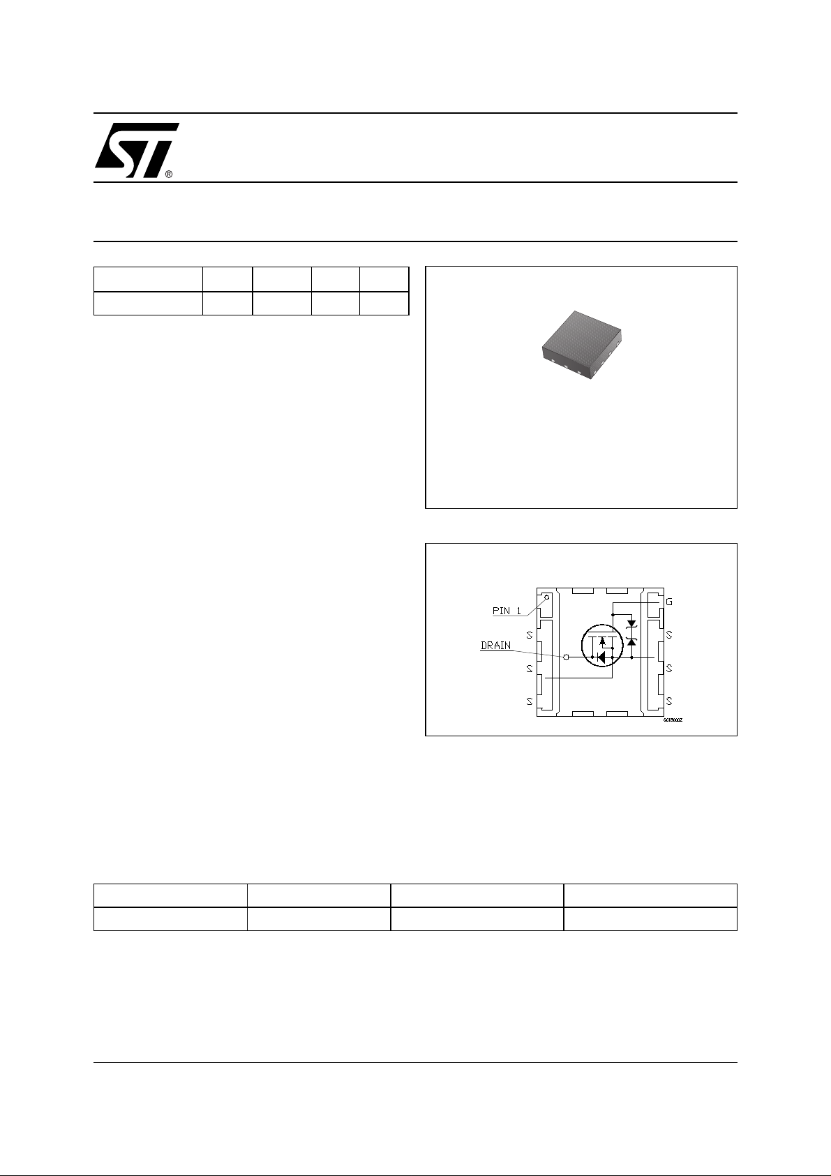
PowerFLAT™(5x5)
(Chip Scale Package)
INTERNAL SCHEMATIC DIAGRAM
APPLICATIONS
■ LIGHTING
■ IDEAL F OR OFF - L IN E POWER SUP PLIE S,
ADAPTORS AND PFC
ORDERING INFORMATION
SALES TYPE MARKING PACKAGE PACKAGING
STL5NK65Z L5NK65Z PowerFLAT™ (5x5) TAPE & REEL
April 2002
1/6
STL5NK65Z
ABSOLUTE MAXIMUM RATINGS
Symbol Parameter Value Unit
V
DS
V
DGR
V
GS
I
(2) Drain Current (continuous) at TC = 25°C (Steady State)
D
I
DM
P
TOT
P
TOT
dv/dt (4) Peak Diode Recovery voltage slope 4.5 V/ns
T
stg
T
THERMA L D ATA
Symbol Parameter Max. Unit
Rthj-F Thermal Resistance Junction-Foot (Drain) 1.67 °C/W
Rthj-amb (2) Thermal Resistance Junction-ambient 50 °C/W
Note: 1. The va l u e i s ra t ed according to R
2. When M ounted on FR-4 Board of 1i nch
3. Pulse wi dth limited by safe operat i ng area
4. I
Drain-source Voltage (VGS = 0)
Drain-gate Voltage (RGS = 20 kΩ)
650 V
650 V
Gate- source Voltage ± 30 V
0.76
Drain Current (continuous) at TC = 100°C
(2)
Drain Current (pulsed) 3 A
0.48
(2) Total Dissipation at TC = 25°C (Steady State) 2.5
(1) Total Dissipation at TC = 25°C (Steady State) 75 W
Derating Factor (2) 0.02 W/°C
Storage Temperature
Max. Operating Junction Temperature
j
<4.2A, di/dt<300A/µs, VDD<V
SD
.
thj-F
(BR)DSS
2
, 2 oz Cu
, TJ<T
JMAX
–55 to 150 °C
A
A
W
AVALANCHE CHARACTERISTICS
Symbol Parameter Max Value Unit
I
AR
E
AS
Avalanche Current, Repetitive or Not-Repetitive
(pulse width limited by T
max)
j
Single Pulse Avalanche Energy
(starting T
= 25 °C, ID = IAR, VDD = 50 V)
j
4.2 A
190 mJ
GATE-SOURCE ZENER DIODE
Symbol Parameter Test Conditions Min. Typ. Max. Unit
BV
GSO
Gate-Source Breakdown
Igs=± 1mA (Open Drain) 30 V
Voltage
PROTECTION FEATURES OF GATE-TO-SOURCE ZENER DIODES
The built-in back-to-back Zener diodes have specifically been designed to enhance not only the device’s
ESD capability, but also to make them safely absorb possible voltage transients that may occasionally be
applied from gate to souce. In this respect the Zener voltage is appropriate to achieve an efficient and costeffective intervention to protect the device’s integrity. These integrated Zener diodes thus avoid the usage
of external components.
2/6
 Loading...