

SGS Thomson Microelectronics STL35NF3LL Datasheet
STL35NF3LL
N-CHANNEL 30V - 0.0055Ω - 35A PowerFLAT™
LOW GATE CHARGE STripFET™ MOSFET
TARGET DATA
TYPE V
DSS
R
DS(on)
I
D
STL35NF3LL 30 V < 0.007 Ω 35 A
■ TYPICAL R
■ IMPROVED DIE-TO-FOOTPRINT RATIO
■ VERY LOW PROFILE PACKAGE
(on) = 0.0055Ω
DS
DESCRIPTION
This Power MOSFET is t he second generation of
STMicroelectronics unique “STripFET™” technology. The resulting transistor shows extremely low onresistance and minimal gate charge. The new PowerFLAT™ package allows a significant reduction in
board space without compromising performance.
APPLICATIONS
■ DC-DC CONVERTERS
■ BATTERY MANAGEMENT IN NOMADIC
EQUIPMENT
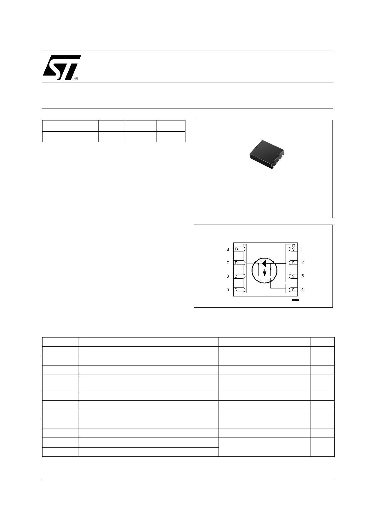
PowerFLAT™(6x5)
(Chip Scale Package)
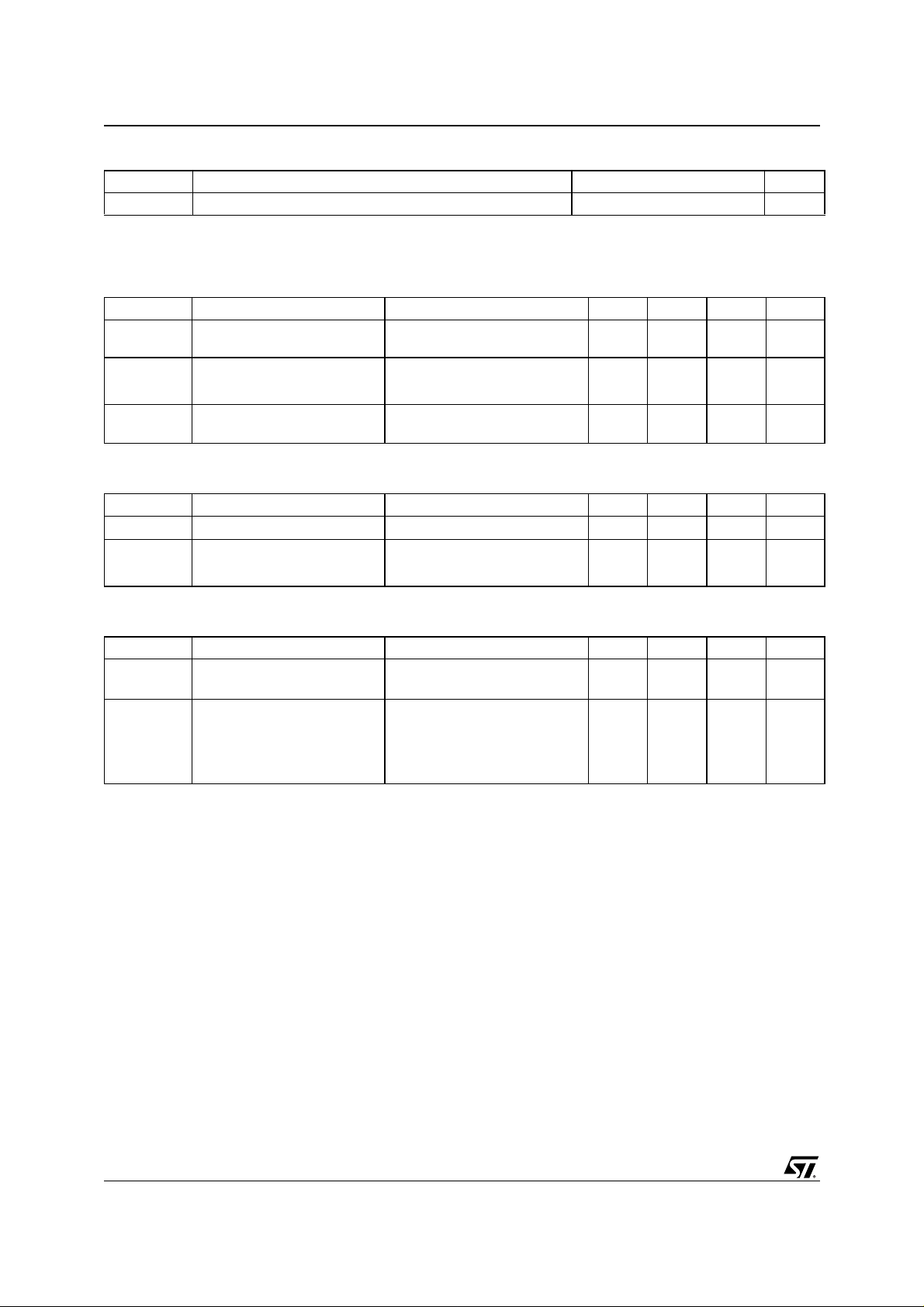
INTERNAL SCHEMATIC DIAGRAM
ABSOLUTE MAXIMUM RATINGS
Symbol Parameter Value Unit
V
DS
V
DGR
V
GS
I
(#) Drain Current (continuos) at TC = 25°C
D
I
DM
P
TOT
dv/dt(1) Peak Diode Recovery voltage slope TBD V/ns
E
AS
T
stg
T
j
(●) Pulse width limited by safe operating area
(#) Limited by Wire Bonding
October 2001
Drain-source Voltage (VGS = 0)
Drain-gate Voltage (RGS = 20 kΩ)
30 V
30 V
Gate- source Voltage ± 15 V
35
Drain Current (continuos) at TC = 100°C
(●)
Drain Current (pulsed) 140 A
Total Dissipation at TC = 25°C
22
80 W
Derating Factor 0.64 W/°C
(2)
Single Pulse Avalanche Energy TBD J
Storage Temperature
Max. Operating Junction Temperature
(1)ISD<35A, di/dt<300A/µs, VDD<V
(2) Starting Tj = 25°C, ID = 30A, VDD = 27.5V
–55 to 150 °C
, TJ<T
(BR)DSS
JMAX
A
A
1/6
STL35NF3LL
THERMA L D ATA
Rthj-case Thermal Resistance Junction-case Max 1.56 °C/W
Rthj-amb Thermal Resistance Junction-ambient Max 50 °C/W
ELECTRICAL CHARACTERISTICS (TCASE = 25 °C UNLESS OTHERWISE SPECIFIED)
OFF
Symbol Parameter Test Conditions Min. Typ. Max. Unit
V
(BR)DSS
Drain-source
Breakdown Voltage
Zero Gate Voltage
Drain Current (V
GS
Gate-body Leakage
Current (V
DS
= 0)
= 0)
ON
I
DSS
I
GSS
(1)
Symbol Parameter Test Conditions Min. Typ. Max. Unit
V
GS(th)
R
DS(on)
Gate Threshold Voltage
Static Drain-source On
Resistance
ID = 250 µA, VGS = 0 30 V
V
= Max Rating
DS
V
= Max Rating, TC = 125 °C
DS
V
= ± 15V ±100 nA
GS
V
= VGS, ID = 250µA
DS
VGS = 10 V, ID = 17.5 A
VGS = 4.5 V, ID = 17.5A
1V
0.0055 0.007 Ω
0.007 0.010 Ω
1µA
10 µA
DYNAMIC
Symbol Parameter Test Conditions Min. Typ. Max. Unit
(1) Forward Transconductance VDS > I
g
fs
C
iss
C
oss
C
rss
Input Capacitance
Output Capacitance 900 pF
Reverse Transfer
Capacitance
ID= 17.5 A
V
DS
x R
D(on)
DS(on)max,
= 25 V, f = 1 MHz, VGS = 0
TBD S
2650 pF
150 pF
2/6
 Loading...