

SGS Thomson Microelectronics STW8NA80, STH8NA80FI Datasheet
STW8NA80
N - CHANNEL ENHANCEMENT MODE
TYPE V
STW8NA80
ST H8NA80FI
■ TYPICALR
■ ± 30V GATE TO SOURCE VOLTAGERATING
■ 100%AVALANCHETESTED
■ REPETITIVEAVALANCHEDATA AT 100
■ LOW INTRINSICCAPACITANCES
■ GATEGHARGEMINIMIZED
■ REDUCEDTHRESHOLD VOLTAGE SPREAD
DS(on)
DSS
800 V
800 V
= 1.3 Ω
DESCRIPTION
This series of POWER MOSFETSrepresents the
most advanced high voltage technology. The optimized cell layout coupled with a new proprietary
edge termination concur to give the device low
RDS(on) and gate charge, unequalled ruggednessand superiorswitchingperformance.
R
DS(on)
<1.50Ω
<1.50Ω
I
D
7.2 A
4.5 A
o
C
STH8NA80FI
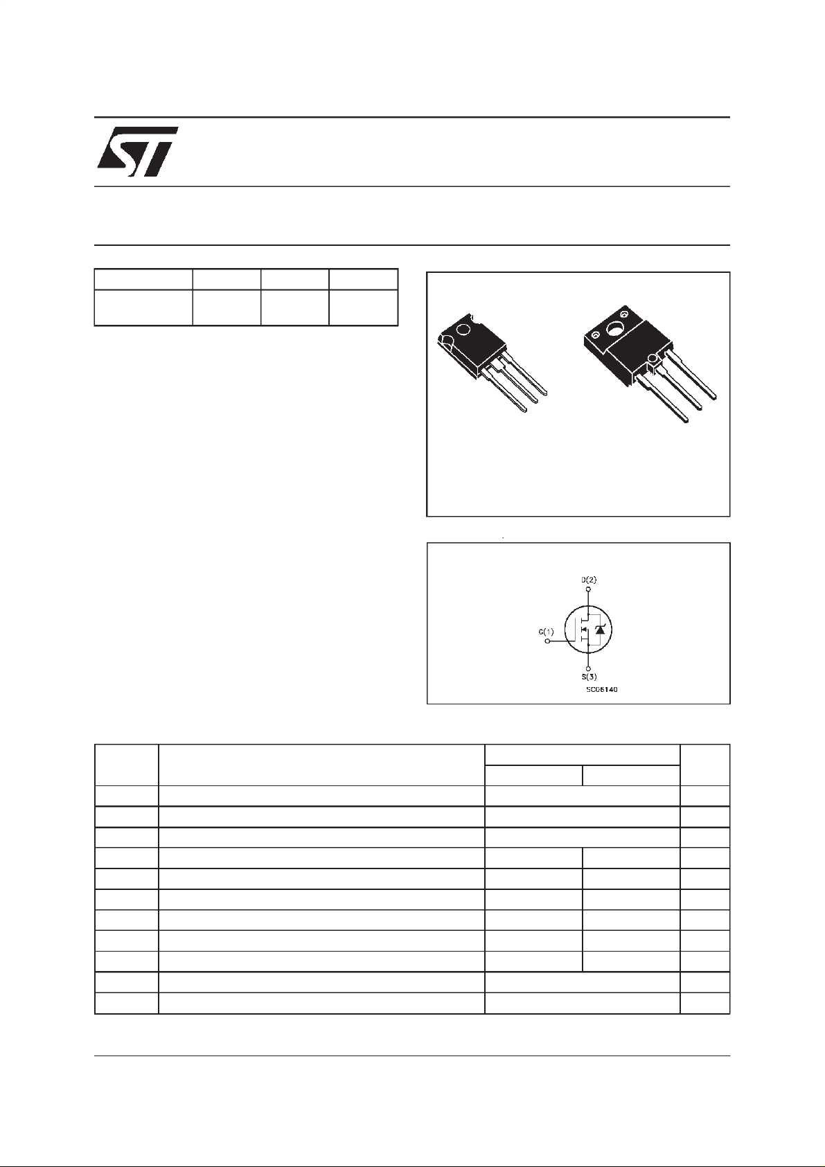
POWER MOS TRANSISTORS
PRELIMINARY DATA
3
2
1
TO-247 ISOWATT218
INTERNAL SCHEMATIC DIAGRAM
3
2
1
APPLICATIONS
■ HIGHCURRENT, HIGH SPEEDSWITCHING
■ SWITCHMODE POWER SUPPLIES (SMPS)
■ DC-AC CONVERTERS FOR WELDING
EQUIPMENTANDUNINTERRUPTIBLE
POWERSUPPLIESAND MOTORDRIVE
ABSOLUTE MAXIMUM RATINGS
Symb o l Parame t er Val ue Unit
ST W8NA80 STH8N A80 F I
V
V
V
I
DM
P
Drain-sourc e Voltage (VGS=0)
DS
Drain- ga t e Voltage (RGS=20kΩ)
DGR
Gate-s ource Voltage
GS
I
Drain Cur rent ( c ont i nuous) at Tc=25oC
D
I
Drain Cur rent ( c ont i nuous) at Tc= 100oC
D
(•)
Drain Cur rent ( puls e d)
Total Dissipation at Tc=25oC
tot
Derating Factor
V
T
(•) Pulse width limited by safe operating area
Ins ula t ion Withst and Volta ge (DC)
ISO
St orage Temper ature
stg
T
Max. Operating Junct ion Temperatu re
j
7.2 4.5 A
4.5 2.8 A
28.8 28.8 A
175 70 W
1.4 0.56 W/
800 V
800 V
± 30 V
4000 V
-65 to 150
150
o
C
o
C
o
C
October 1998
1/6
STW8NA80 STH8NA80FI
THERMAL DATA
TO-247 ISOWATT218
R
thj-case
R
thj-amb
R
thc-sink
T
Ther mal Resistanc e Junct ion-case Max
Ther mal Resistanc e Junct ion-ambient Max
Ther mal Resistanc e Case-sink Ty p
Maximum Lead T e m pe ra t ure For Soldering P urpose
l
AVALANCHE CHARACTERISTICS
Symbol Parameter Max V alue Unit
I
AR
E
Avalanche C urrent, Repetitive or Not-Repetitive
(pulse width limited by T
Single Pul se Avalanc he Ener gy
AS
(starting T
=25oC, ID=IAR,VDD=50V)
j
max,δ <1%)
j
0.71 1.78
30
0.1
300
7.2 A
700 mJ
o
C/W
o
C/W
o
C/W
o
C
ELECTRICAL CHARACTERISTICS
=25oC unless otherwisespecified)
(T
case
OFF
Symbol Parameter Test Conditions Min. Typ. Max. Unit
V
(BR)DSS
I
DSS
I
GSS
Drain-source
Break dow n Vo lt age
Zero Gate Voltage
Drain Curre nt (V
GS
Gat e- bod y Leakag e
Current (V
DS
=0)
=0)
=250µAVGS=0
I
D
V
=MaxRating
DS
=MaxRating Tc= 100oC
V
DS
V
= ± 30 V
GS
800 V
50
500
100 nA
ON(∗)
Symbol Parameter Test Conditions Min. Typ. Max. Unit
V
GS(th)
R
DS(on)
I
D(on)
Gate Threshold Voltage VDS=VGSID= 250µA
Sta t ic Drain-s our c e On
Resistance
On State Drain Current
V
=10V ID=4A
GS
V
DS>ID(on)xRDS(on)max
VGS=10V
2.25 3 3.75 V
1.3 1. 5
7.2 A
DYNAMIC
Symbol Parameter Test Conditions Min. Typ. Max. Unit
g
(∗)Forward
fs
Tr ansc on duc tance
C
C
C
Input Capaci t ance
iss
Out put Capac itance
oss
Reverse Transfer
rss
Capacit a nc e
V
DS>ID(on)xRDS(on)maxID
=25V f=1MHz VGS=0
V
DS
=4A
4.5 7.9 S
1750
188
50
2300
245
70
µA
µA
Ω
pF
pF
pF
2/6
 Loading...