

SGS Thomson Microelectronics STW8NA60, STH8NA60FI Datasheet
STW8NA60
N - CHANNEL ENHANCEMENT MODE
FAST POWER MOS TRANSISTOR
TYPE V
STW8NA60
ST H8NA60FI
■ TYPICALR
■ ± 30V GATE TO SOURCE VOLTAGERATING
■ 100%AVALANCHETESTED
■ REPETITIVEAVALANCHEDATA AT 100
■ LOW INTRINSICCAPACITANCES
■ GATECHARGE MINIMIZED
■ REDUCEDTHRESHOLD VOLTAGE SPREAD
DS(on)
DSS
600 V
600 V
= 0.92 Ω
APPLICATIONS
■ HIGHCURRENT, HIGH SPEEDSWITCHING
■ SWITCHMODE POWER SUPPLIES (SMPS)
■ DC-AC CONVERTERS FOR WELDING
EQUIPMENTANDUNINTERRUPTIBLE
POWERSUPPLIESAND MOTORDRIVE
R
DS(on)
< 1 Ω
< 1 Ω
I
D
8A
5A
o
C
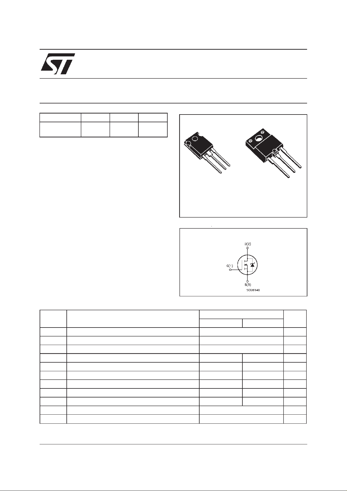
STH8NA60FI
3
2
1
TO-247 ISOWATT218
INTERNAL SCHEMATIC DIAGRAM
1
3
2
ABSOLUTE MAXIMUM RATINGS
Symb o l Parameter Value Uni t
ST W 8N A60 ST H8 NA6 0F I
V
V
V
I
DM
P
V
T
(•) Pulse width limited by safe operating area
October 1998
Dra in- sour c e Volt age (VGS= 0) 600 V
DS
Dra in- gat e Voltage (RGS=20kΩ) 600 V
DGR
Gat e-source Voltage
GS
I
Dra in Cu rr ent (contin uous ) a t Tc=25oC85A
D
I
Dra in Cu rr ent (contin uous ) a t Tc=100oC5.13.2A
D
30 V
±
(•) Dra in Cu rr ent (pulsed) 32 32 A
Tot al Dissipat ion at Tc=25oC 150 60 W
tot
Der ati ng Fact or 1.2 0.48 W/
Insulation Withstand Voltage (DC) 4000 V
ISO
St orage Temperat ure -65 to 150
stg
T
Max. Operating Junct ion Temperat ure 150
j
o
C
o
C
o
C
1/10
STW8NA60-STH8NA60FI
THERMAL DATA
TO-247 ISOWATT218
R
thj-case
R
thj-amb
R
thc-sink
T
AVALANCHE CHARACTERISTICS
Symbol Parameter Max V alue Unit
I
AR
E
Ther mal Resistanc e Junct ion-case Ma x 0.83 2.08
Ther mal Resistanc e Junct ion-ambient Max
Ther mal Resistanc e Case-sink Ty p
Maximum Lead T e m pe ra t ure For Soldering P urpose
l
Avalanche C urrent, R epetitive or Not-Repetitive
(pulse width limited by T
Single Pul se Avalanc he Ener gy
AS
(starting T
=25oC, ID=IAR,VDD=50V)
j
max,δ <1%)
j
30
0.1
300
8A
480 mJ
o
C/W
o
C/W
o
C/W
o
C
ELECTRICAL CHARACTERISTICS
=25oC unless otherwisespecified)
(T
case
OFF
Symbol Parameter Test Conditions Min. Typ. Max. Unit
V
(BR)DSS
Drain-source
ID=250µAVGS= 0 600 V
Break dow n Vo lt age
I
DSS
I
GSS
Zero Gate Voltage
Drain Curre nt (V
GS
Gat e- bod y Leakag e
Current (V
DS
=0)
=0)
V
=MaxRating
DS
=MaxRating Tc= 100oC
V
DS
V
=± 30 V
GS
25
250
100 nA
±
ON(∗)
Symbol Parameter Test Conditions Min. Typ. Max. Unit
V
GS(th)
R
DS(on)
Gate Threshold Voltage VDS=VGSID= 250µA2.2533.75V
Sta t ic Drain-s our c e On
VGS=10V ID=4A 0.92 1
Resistance
I
D(on)
On State Drain Current VDS>I
D(on)xRDS(on)max
8A
VGS=10V
DYNAMIC
Symbol Parameter Test Conditions Min. Typ. Max. Unit
g
(∗)Forward
fs
Tr ansc on duc tance
C
C
C
Input Capaci t ance
iss
Out put Capac itance
oss
Reverse Transfer
rss
Capacit a nc e
VDS>I
D(on)xRDS(on)maxID
=4A 4.5 6.6 S
VDS=25V f=1MHz VGS= 0 1350
175
45
1690
230
60
µA
µA
Ω
pF
pF
pF
2/10
STW8NA60-STH8NA60FI
ELECTRICAL CHARACTERISTICS
(continued)
SWITCHINGON
Symbol Parameter Test Conditions Min. Typ. Max. Unit
t
d(on)
t
r
Turn-on Time
Rise Time
VDD=300V ID=4A
R
=4.7
G
Ω
VGS=10V
20
35
28
35
(see test circuit, figure 3)
(di/dt)
Tur n-on Current Slope VDD=480V ID=8A
on
R
G
=47
Ω
VGS=10V
200 A/µ s
(see test circuit, figure 5)
Q
Q
Q
Tot al Gate Charge
g
Gat e- Source Charge
gs
Gate-Drain Charge
gd
VDD= 480 V ID=8A VGS=10V 58
9
27
82 nC
SWITCHINGOFF
Symbol Parameter Test Conditions Min. Typ. Max. Unit
t
r(Voff)
t
t
Off-voltage Ris e Time
Fall T ime
f
Cross-over Tim e
c
VDD=640V ID=8A
=4.7 Ω VGS=10V
R
G
(see test circuit, figure 5)
16
16
26
23
23
37
SOURCEDRAINDIODE
Symbol Parameter Test Conditions Min. Typ. Max. Unit
I
SD
I
SDM
V
SD
t
Q
I
RRM
(∗) Pulsed:Pulse duration = 300 µs, duty cycle 1.5 %
(•) Pulse width limited by safe operatingarea
Source-drain Current
(•)
Source-drain Current
8
32
(pulsed)
(∗)ForwardOnVoltage ISD=8A VGS=0 1.6 V
Reverse Recovery
rr
Time
Reverse Recovery
rr
ISD=8A di/dt=100A/µs
= 100 V Tj=150oC
V
DD
(see test circuit, figure 5)
600
10
Charge
Reverse Recovery
33
Current
ns
ns
nC
nC
ns
ns
ns
A
A
ns
µC
A
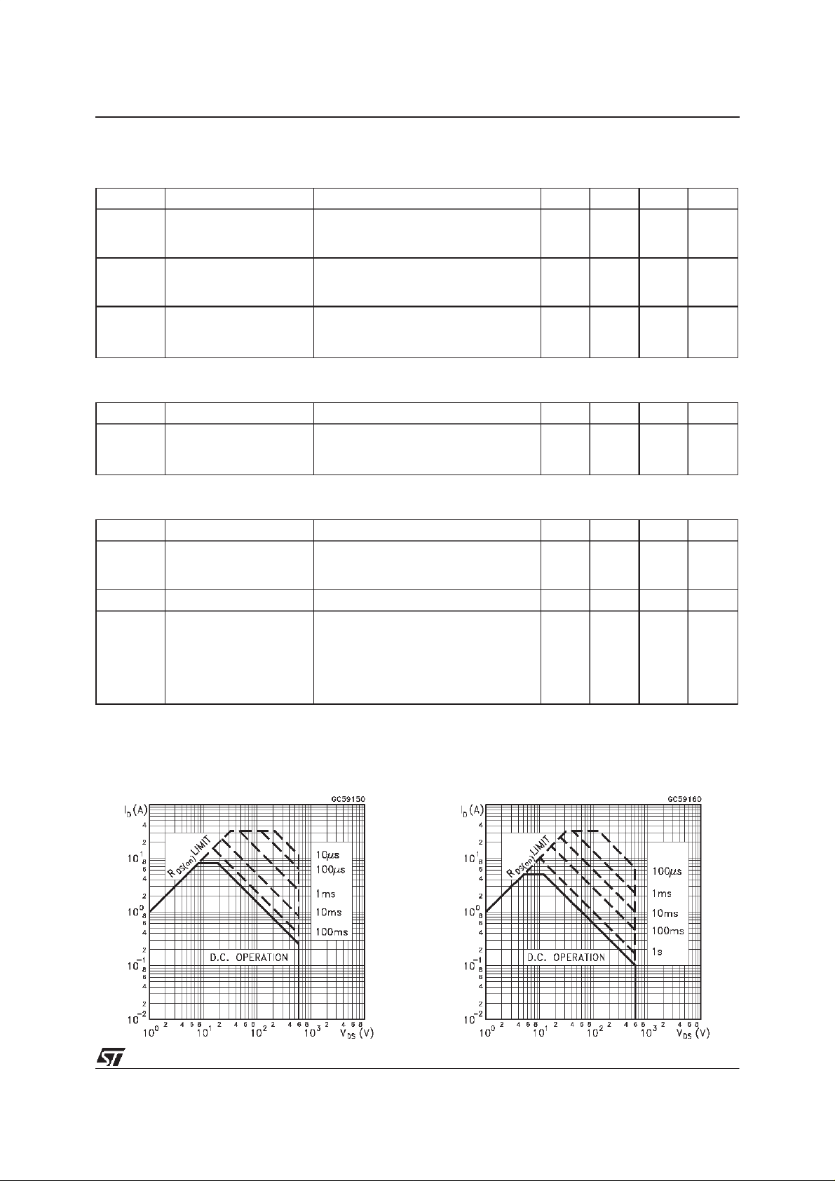
SafeOperating Area for TO-247 Safe OperatingArea for ISOWATT218
3/10
 Loading...