

SGS Thomson Microelectronics STGY50NB60HD Datasheet
N-CHANNEL 50A - 600V MAX247
TYPE V
CES
ST G Y50NB60H D 600 V < 2.8 V 50 A
■ HIGHINPUTIMPEDANCE
(VOLTAGEDRIVEN)
■ LOW ON-VOLTAGEDROP(V
■ LOW GATE CHARGE
■ HIGHCURRENT CAPABILITY
■ VERYHIGH FREQUENCYOPERATION
■ OFFLOSSES INCLUDE TAIL CURRENT
■ CO-PACKAGEDWITHTURBOSWITCH
ANTIPARALLELDIODE
DESCRIPTION
Using the latest high voltage technology based
on a patented strip layout, STMicroelectronics
has designed an advanced family of IGBTs, the
PowerMESH
IGBTs, with outstanding
perfomances. The suffix ”H” identifies a family
optimized to achieve very low switching times for
high frequency applications (<120kHz).
V
CE(sat)
CESAT
I
C
)
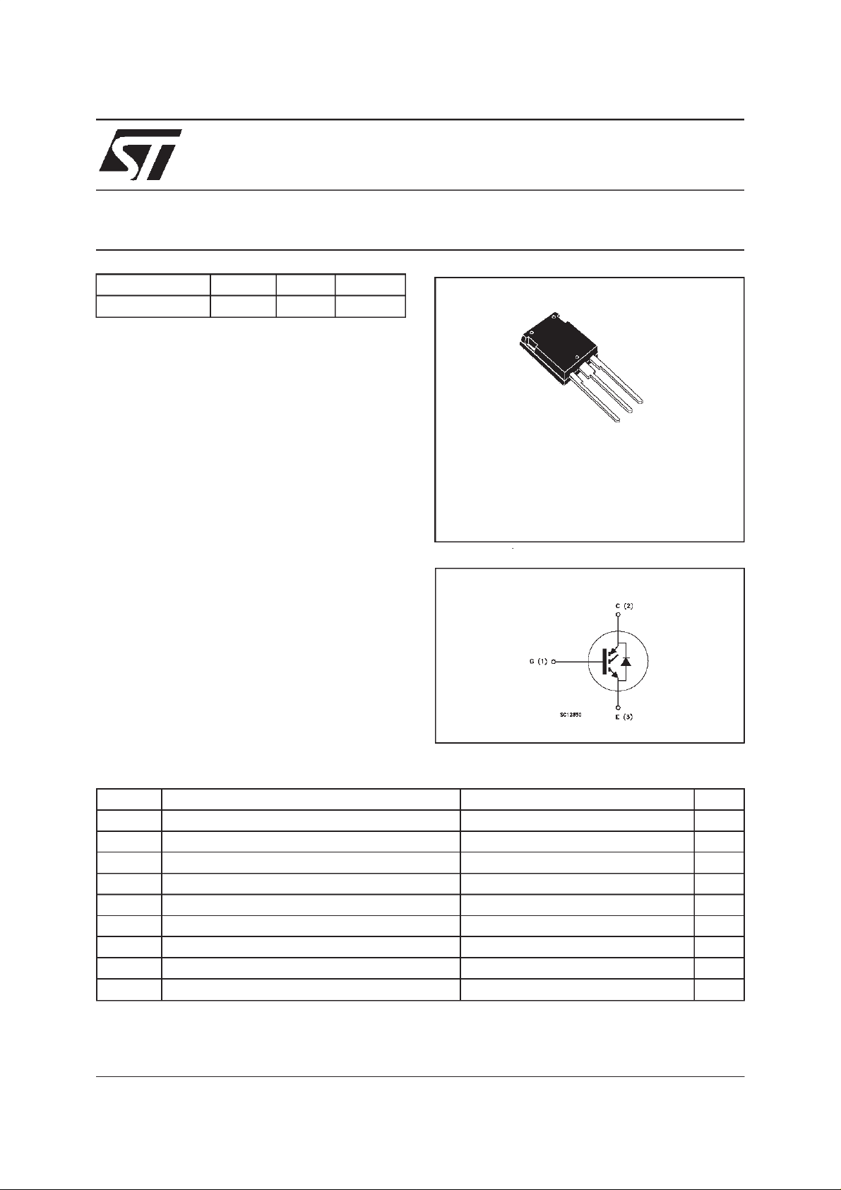
STGY50NB60HD
PowerMESH IGBT
PRELIMINARY DATA
3
2
1
MAX247
INTERNAL SCHEMATIC DIAGRAM
APPLICATIONS
■ HIGHFREQUENCYMOTORCONTROLS
■ WELDINGEQUIPMENTS
■ SMPSAND PFC IN BOTH HARD SWITCH
AND RESONANTTOPOLOGIES
ABSOLUTE MAXIMUM RATINGS
Symbol Parameter Value Unit
V
V
I
CM
P
T
(•) Pulse width limited by safe operating area
Collect o r -Em i t t er Volt age (VGS= 0) 600 V
CES
Gate-Emitter Voltage ± 20 V
GE
I
Collect o r Current (continuo us ) at Tc=25oC 100 A
C
I
Collect o r Current (continuo us ) at Tc= 100oC50A
C
(•) Collect o r Current (pul s ed) 400 A
Tot al Dis sipation at Tc=25oC 250 W
tot
Derat ing Fact or 2 W/
Sto rage Tem perature -65 t o 15 0
stg
T
Max. O per a t ing J unction T emperature 150
j
o
C
o
C
o
C
June 1999
1/6
STGY50NB60HD
THERMAL DATA
R
thj-case
R
thj-amb
R
thc-h
Ther mal Resistanc e Junct ion-case Max
Ther mal Resistanc e Junct ion-ambie nt Max
Ther mal Resistanc e Case-heatsink Typ
0.5
30
0.1
o
C/W
oC/W
o
C/W
ELECTRICAL CHARACTERISTICS
=25oC unless otherwisespecified)
(T
j
OFF
Sym bol Param e t er Test Condit ion s Min . Typ. Max. Unit
V
BR(CES)
Collector-Emitter
IC=250µAVGE= 0 600 V
Break dow n Voltage
I
I
ON (∗
CES
GES
Collect o r cut-off
=0)
(V
GE
Gat e- Em i t t er Lea kage
Current (V
)
CE
=0)
V
=MaxRating Tj=25oC
CE
=MaxRating Tj=125oC
V
CE
V
= ± 20 V VCE=0 ±100 nA
GE
100
1000
Sym bol Param e t er Test Condit ion s Min . Typ. Max. Unit
V
GE(th)
Gate Threshold
VCE=VGEIC= 250 µA35V
Voltage
V
CE(SAT)
Collector-Emitter
Sat urat ion Voltage
VGE=15V IC=50A
V
=15V IC=50A Tj= 125oC
GE
2.3
1.9
2.8 V
DYNAMIC
Sym bol Param e t er Test Condit ion s Min . Typ. Max. Unit
C
C
C
Q
Q
g
Q
I
CL
Forward
fs
Tr ansc on duc tance
Input Capac i t ance
ies
Out put Capacitance
oes
Reverse Tr ansfer
res
Capacit a nc e
Tot al Gat e Charge
G
Gate-Emitt er Charge
GE
Gat e- Col lect or C har ge
GC
Latc hing C ur rent V
VCE=25 V IC=50A 22 S
VCE=25V f=1MHz VGE= 0 4500
450
90
VCE= 480 V IC=50A VGE= 15 V 260
28
15
=480V RG=10 Ω
clamp
T
= 150oC
j
200 A
µA
µ
V
pF
pF
pF
nC
nC
nC
A
SWITCHINGON
Sym bol Param e t er Test Condit ion s Min . Typ. Max. Unit
(di/dt)
2/6
t
d(on)
t
r
Eon(❍)
Delay T ime
Rise Ti me
Tur n-on Current Slop e
on
Turn-on
Switching Losses
VCC= 480 V IC=50A
=15V RG=10Ω
V
GE
V
=480V IC=50A
CC
=10Ω VGE=15V
R
G
T
=125oC
j
20
70
350
950
ns
ns
A/µs
J
µ
 Loading...