

SGS Thomson Microelectronics STGW50NB60H Datasheet
®
N-CHANNEL 50A - 600V TO-247
TYPE V
CES
STGW50NB60H 600 V < 2.8 V 50 A
■
HIGH INPUT IMPEDANCE
(VOLTAGE DRIVEN)
■
LOW ON-VOLTAGE DROP (V
■
LOW GATE CHARGE
■
HIGH CURRENT CAPABILITY
■
VERY HIGH FREQUENCY OPERATION
■
OFF LOSSES INCLUDE TAIL CURRENT
DESCRIPTION
Using the latest high voltage technology based
on a patented strip layout, STMicroelectronics
has designed an advanced family of IGBTs, the
PowerMESH IGBTs, with outstanding
perfomances. The suffix "H" identifies a family
optimized to achieve very low switching times for
high frequency applications (<120kHz).
APPLICATIONS
■
HIGH FREQUENCY MOTOR CONTROLS
■
WELDING EQUIPMENTS
■
SMPS AND PFC IN BOTH HARD SWITCH
AND RESONANT TOPOLOGIES
V
CE(sat)
CESAT
I
C
)
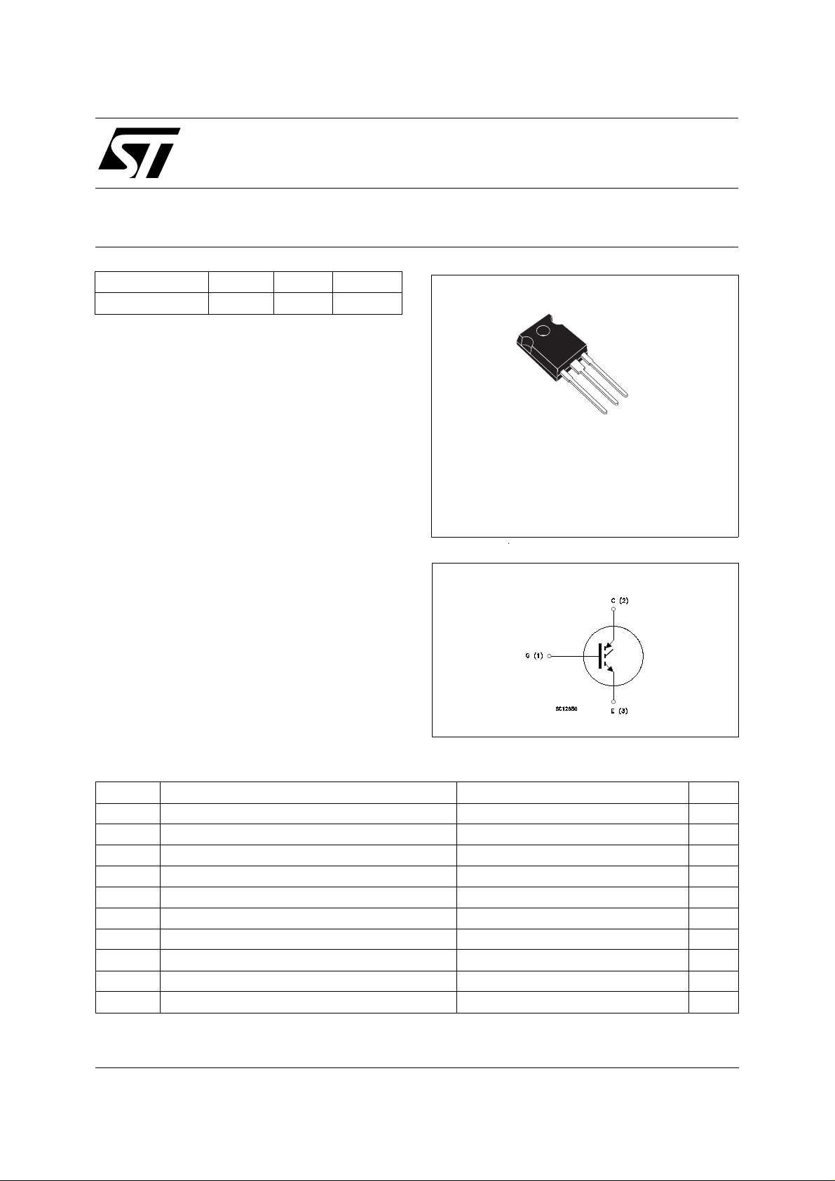
STGW50NB60H
PowerMESH IGBT
PRELIMINARY DATA
3
2
1
TO-247
INTERNAL SCHEMATIC DIAGRAM
ABSOLUTE MAXIMUM RATINGS
Symbol Parameter Value Unit
V
V
V
I
CM
P
T
(•) Pulse width limited by safe operating area
June 1999
Collector-Emitter Voltage (VGS = 0) 600 V
CES
Emitter-Collector Voltage 20 V
ECR
Gate-Emitter Voltage ± 20 V
GE
I
Collector Current (continuous) at Tc = 25 oC100A
C
I
Collector Current (continuous) at Tc = 100 oC50A
C
(•) Collector Current (pulsed) 400 A
Total Dissipation at Tc = 25 oC250W
tot
Derating Factor 2 W/
Storage Temperature -65 to 150
stg
T
Max. Operating Junction Temperature 150
j
o
C
o
C
o
C
1/5
STGW50NB60H
THERMAL DATA
R
thj-case
R
thj-amb
R
thc-h
Thermal Resistance Junction-case Max
Thermal Resistance Junction-ambient Max
Thermal Resistance Case-heatsink Typ
0.5
30
0.1
o
C/W
oC/W
o
C/W
ELECTRICAL CHARACTERISTICS
= 25 oC unless otherwise specified)
(T
j
OFF
Symbol Parameter Test Conditions Min. Typ. Max. Unit
V
BR(CES)
Collector-Emitter
IC = 250 µA V
= 0 600 V
GE
Breakdown Voltage
I
I
CES
GES
Collector cut-off
(V
= 0)
GE
Gate-Emitter Leakage
Current (V
CE
= 0)
= Max Rating Tj = 25 oC
V
CE
V
= Max Rating Tj = 125 oC
CE
= ± 20 V VCE = 0 ± 100 nA
V
GE
10
100
ON (∗)
Symbol Parameter Test Conditions Min. Typ. Max. Unit
V
GE(th)
Gate Threshold
V
= VGE IC = 250 µA35V
CE
Voltage
V
CE(SAT)
Collector-Emitter
Saturation Voltage
VGE = 15 V IC = 50 A
V
= 15 V IC = 50 A Tj = 125 oC
GE
2.3
1.9
2.8 V
DYNAMIC
Symbol Parameter Test Conditions Min. Typ. Max. Unit
g
C
C
C
Q
Q
Q
I
CL
Forward
fs
Transconductance
Input Capacitance
ies
Output Capacitance
oes
Reverse Transfer
res
Capacitance
Total Gate Charge
G
Gate-Emitter Charge
GE
Gate-Collector Charge
GC
Latching Current V
VCE =25 V IC = 50 A 22 S
V
= 25 V f = 1 MHz V
CE
= 0 4500
GE
450
90
VCE = 480 V IC = 50 A VGE = 15 V 260
28
115
= 480 V RG=10 Ω
clamp
V
= 15 V Tj = 150 oC
GE
200 A
µA
µA
V
pF
pF
pF
nC
nC
nC
SWITCHING ON
Symbol Parameter Test Conditions Min. Typ. Max. Unit
30
90
350
600
2/5
t
d(on)
t
r
(di/dt)
E
on
Delay Time
Rise Time
Turn-on Current Slope
on
Turn-on
Switching Losses
VCC = 480 V IC = 50 A
V
= 15 V RG = 10Ω
GE
V
= 480 V IC = 50 A
CC
R
= 10 Ω VGE = 15 V
G
T
= 125 oC
j
ns
ns
A/µs
µJ
 Loading...