

SGS Thomson Microelectronics STGP7NB60HD, STGP7NB60HDFP Datasheet
STGP7NB60HD
N-CHANNEL 7A - 600V TO-220/FP
TYPE V
ST G P7NB60HD
ST G P7NB60HDFP
■ HIGHINPUT IMPEDANCE
CES
600 V
600 V
(VOLTAGEDRIVEN)
■ LOW ON-VOLTAGEDROP (V
■ LOW GATECHARGE
■ HIGHCURRENTCAPABILITY
■ VERYHIGH FREQUENCYOPERATION
■ OFFLOSSES INCLUDETAIL CURRENT
■ CO-PACKAGEDWITH TURBOSWITCH
ANTIPARALLELDIODE
DESCRIPTION
Using the latest high voltage technology based
on a patented strip layout, STMicroelectronics
has designed an advanced family of IGBTs, the
PowerMESH IGBTs, with outstanding
perfomances. The suffix ”H” identifies a family
optimized to achieve very low switching times for
high frequencyapplications(<120kHz).
V
CE(sat)
I
C
<2.8V
<2.8V7A7A
)
cesat
STGP7NB60HDFP
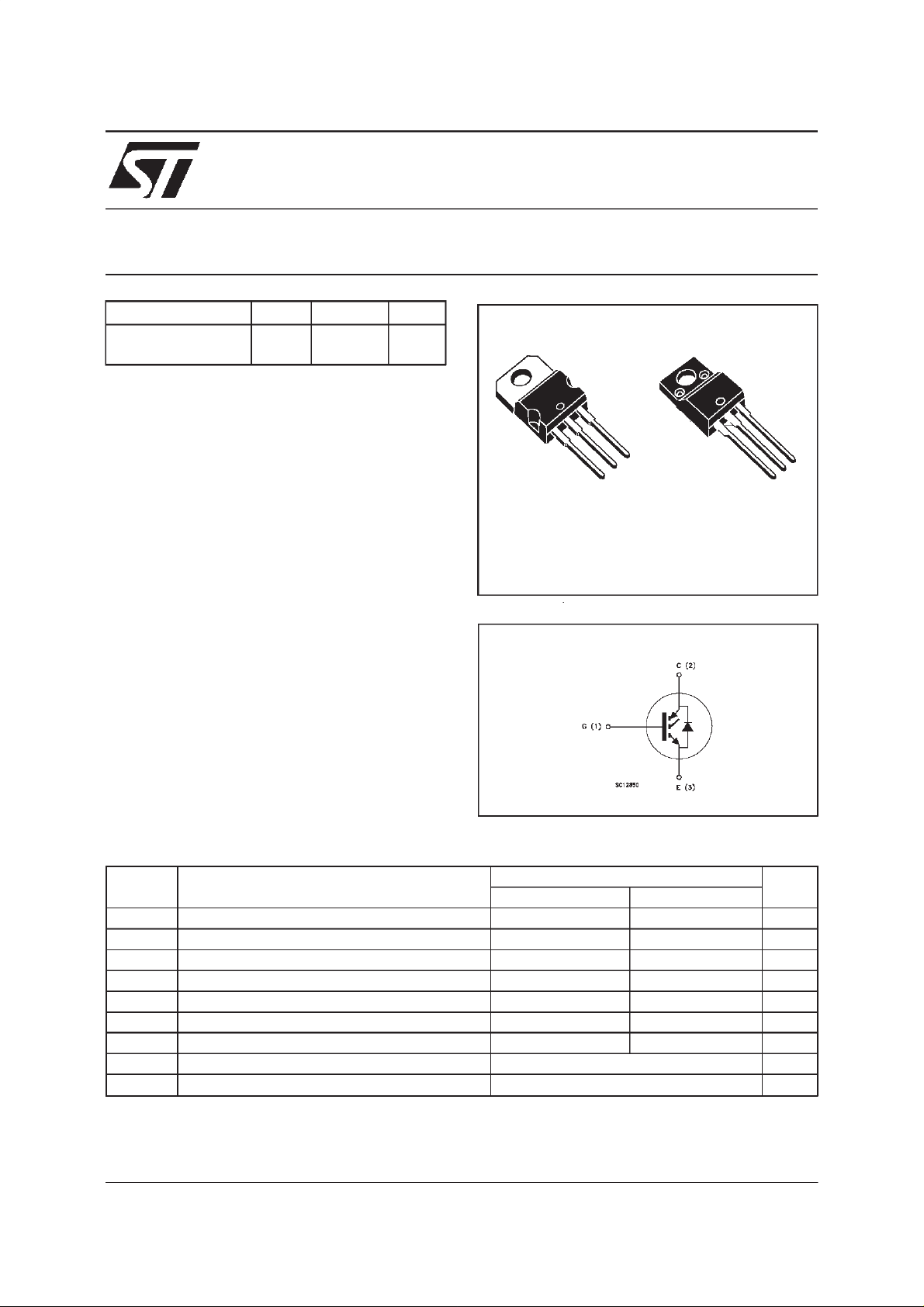
PowerMESH IGBT
3
2
1
TO-220 TO-220FP
INTERNAL SCHEMATIC DIAGRAM
3
2
1
APPLICATIONS
■ HIGHFREQUENCY MOTOR CONTROLS
■ SMPSAND PFC IN BOTH HARDSWITCH
AND RESONANTTOPOLOGIES
ABSOLUTE MAXIMUM RATINGS
Sym bol Parame t er Value Unit
STGP7NB60HD ST G P7 NB 60H DF P
V
V
I
CM
P
T
(•) Pulse widthlimited by safe operating area
June 1999
Collec t or -Emitte r Volt age (VGS = 0) 600 600 V
CES
Gate-Emitter Voltage ± 20 ± 20 V
GE
Collec t or Curr e nt (contin uous) at Tc = 25oC14 13A
I
C
Collec t or Curr e nt (contin uous) at Tc = 100oC7 6 A
I
C
(•) Collec t or Curr e nt (pulsed) 56 56 A
Total Dissipation at Tc = 25oC8035W
tot
Derat i ng Fac t or 0.64 0. 28 W/
St orage Tem p er at u re -65 to 150
stg
Max. Operat ing Junct ion Temp er at u re 150
T
j
o
C
o
C
o
C
1/9

STGP7NB60HD/FP
THERMAL DATA
R
thj-case
R
thj-amb
R
thc-sink
Ther mal Resistanc e Junct ion-case Max 1.56 3.57
Ther mal Resistanc e Junct ion-ambient Max
Ther mal Resistanc e Case-sink Ty p
TO-220 TO- 220FP
62.5
0.5
o
C/W
o
C/W
o
C/W
ELECTRICAL CHARACTERISTICS
=25oC unless otherwise specified)
(T
j
OFF
Sym bol Parame t er Test Conditions M in. Typ. Max. U nit
V
BR(CES)
Collector-Emitter
IC=250µAVGE= 0 600 V
Break dow n Volt age
I
I
CES
GES
Collect o r cut - off
=0)
(V
GE
Gat e- Em i t t er Leakage
Current (V
CE
=0)
V
=MaxRating Tj=25oC
CE
=MaxRating Tj=125oC
V
CE
= ± 20 V VCE=0 ±100 nA
V
GE
250
2000µAµA
ON(∗)
Sym bol Parame t er Test Conditions M in. Typ. Max. U nit
V
GE(th)
Gate Th reshold
VCE=VGEIC= 250 µ A35V
Voltage
V
CE(SAT)
Collector-Emitter
Sat urat ion Volt age
VGE=15V IC=7A
=15V IC=7A Tj=125oC
V
GE
2.3
1.9
2.8 V
DYNAMIC
Sym bol Parame t er Test Conditions M in. Typ. Max. U nit
C
C
C
Q
Q
g
Q
I
CL
Forward
fs
Tr ansc on duc tance
Input Capacitanc e
ies
Out put Capacitance
oes
Reverse Transfer
res
Capacit a nc e
Tot al Gate Charge
G
Gate-Emitt er C harge
GE
Gat e- Col lect or C har ge
GC
Latc hing Curr ent V
VCE=25 V IC=7A 3.5 5 S
VCE=25V f=1MHz VGE= 0 390
45
10
VCE= 480 V IC=7A VGE=15V 42
560
68
15
730
90
20
55 nC
7.9
17.6
=480V RG=10Ω
clamp
T
= 150oC
j
28 A
V
pF
pF
pF
nC
nC
SWITCHINGON
Sym bol Parame t er Test Conditions M in. Typ. Max. U nit
(di/dt)
2/9
t
d(on)
t
r
Eon(❍)
Delay Time
Rise Time
Tur n-on Current Slope
on
Turn-on
Switching Losses
VCC= 480 V IC=7A
=15V RG=10Ω
V
GE
V
=480V IC=7A
CC
=10Ω VGE=15V
R
G
T
=125oC
j
15
48
160
185
ns
ns
A/µs
J
µ
STGP7NB60HD/FP
ELECTRICAL CHARACTERISTICS
(continued)
SWITCHINGOFF
Sym bol Parame t er Test Conditions M in. Typ. Max. U nit
tr(v
t
E
E
tr(v
t
E
E
t
d(off
off
ts
t
d(off
off
ts
Cross-Over Time
c
Off Voltage Rise Time
)
off
)
Delay Time
t
Fall T ime
f
(**)
Turn-off Switching Loss
(❍)
Tot al Switching Loss
Cross-Over Time
c
Off Voltage Rise Time
)
off
Delay Time
)
Fall T ime
t
f
Turn-off Switching Loss
(**)
(❍)
Tot al Switching Loss
V
=480V IC=7A
CC
R
=10
Ω
=480V IC=7A
=10
Ω
= 125oC
V
R
T
GE
CC
GE
j
VGE=15V
VGE=15V
85
20
75
70
85
235
150
50
110
110
220
405
COLLECTOR-EMITTERDIODE
Sym bol Param e t er Tes t Conditions Min . Typ. Max. Unit
I
For ward Current
f
I
V
t
Q
I
rrm
(•) Pulse width limited by max. junction temperature
(
❍) Include recovery lossess on the STTA506 freewheeling diode
(∗) Pulsed: Pulse duration= 300µs, duty cycle 1.5%
(**)Losses Include Also The Tail (Jedec Standardization)
For ward Current pulsed
fm
For ward On- Voltage If=7A
f
Reverse Recovery Time
rr
Reverse Recovery Charge
rr
Reverse Recovery Current
=7A Tj= 125oC
I
f
If=7A VR=200 V
dI/dt = 100 A/µST
= 125oC
j
1.6
1.4
100
180
3.6
7
56
2.0 V
ns
ns
ns
ns
µJ
µ
ns
ns
ns
ns
µ
µ
J
J
J
A
A
V
ns
nC
A
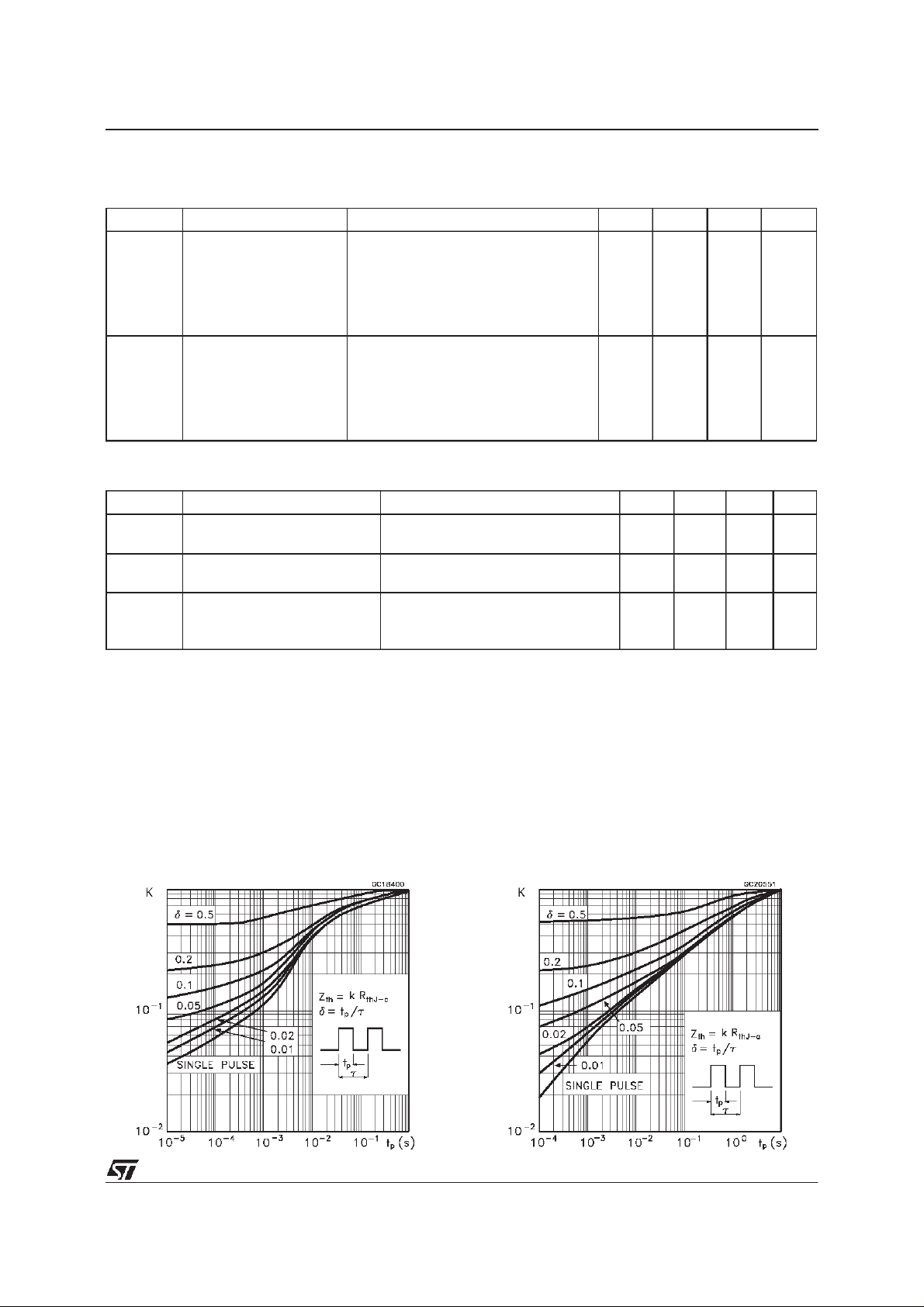
ThermalImpedeanceFor TO-220 ThermalImpedeanceFor TO-220FP
3/9
 Loading...