

SGS Thomson Microelectronics STGP7NB120SD Datasheet
STGP7NB120SD
N-CHANNEL 7A - 1200V -TO-220
PowerMESH™ IGBT
TYPE V
CES
V
CE(sat)
I
C
STGP7NB120SD 1200 V < 2.1 V7A
■ HIGH INPUT IMPEDANCE (VOLTAGE DRIVEN)
■ VERY LOW ON-VOLTAGE DROP (V
■ OFF LOSSES INCLUDE TAIL CURRENT
■ HIGH CURRENT CAPABILITY
cesat
)
DESCRIPTION
Using the lates t high voltage technology based on a
patented strip layout, STMicroelectronics has
designed an advanced family of IGBTs, the
PowerMESH
™
IGBTs, with outstanding
performances. The suffix “S” identifies a f amily
optimized achieve minimum on-v oltage drop for low
frequency applications (<1kHz).
APPLICATIONS
■ MOTOR CONTROL
■ LIGHT DIMMER
■ INTRUSH CURRENT LIMITATION
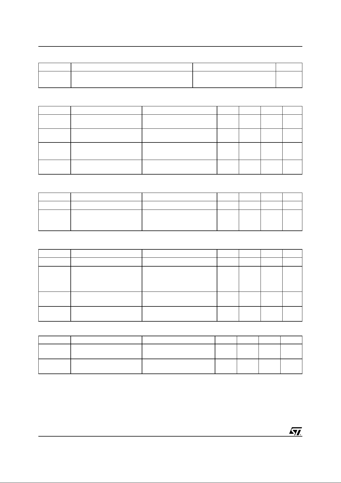
3
2
1
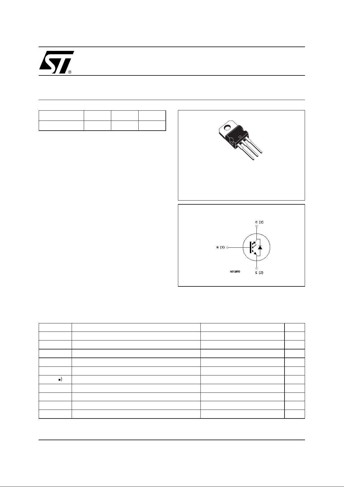
TO-220
INTERNAL SCHEMATIC DIAGRAM
ABSOLUTE MAXIMUM RATINGS
Symbol Parameter Value Unit
V
CES
V
ECR
V
GE
I
C
I
C
I
CM
P
TOT
T
stg
T
j
Collector-Emitter Voltage (VGS=0)
1200 V
Reverse Battery Protection 20 V
Gate-Emitter Voltage ±20 V
Collector Current (continuous) at TC=25°C
Collector Current (continuous) at TC=100°C
()
Collector Current (pulsed) 20 A
Total Dissipation at TC= 25°C
10 A
7A
90 W
Derating Factor 0.7 W/°C
Storage Temperature –65 to 150 °C
Max. Operating Junction Temperature 150 °C
(●) Pulsewidthlimited by safeoperatingarea
1/8November 2002
STGP7NB120SD
THERMAL DATA
Rthj-case Thermal Resistance Junction-case Max 1.38 °C/W
Rthj-amb Thermal Resistance Junction-ambient Max 62.5 °C/W
Rthc-h Thermal Resistance Case-heatsink Typ 0.5 °C/W
ELECTRICAL CHARACTERISTICS (T
= 25 °C UNLESS O THERWISE SPECIFIED)
CASE
OFF
Symbol Parameter Test Conditions Min. Typ. Max. Unit
V
BR(CES)
Collector-Emitter Breakdown
IC= 250 µA, VGE= 0 1200 V
Voltage
V
BR(ECR)
Emitter-Collector Breakdown
IC= 10mA, VGE= 0 20 V
Voltage
I
CES
I
GES
Collector cut-off
=0)
(V
GE
Gate-Emitter Leakage
Current (V
CE
=0)
V
= Max Rating, TC=25°C
CE
VCE= Max Rating, TC= 125 °C
V
=±20V,VCE= 0 ±100 nA
GE
50 µA
250 µA
ON (1)
Symbol Parameter Test Conditions Min. Typ. Max. Unit
V
GE(th)
V
CE(sat)
Gate Threshold Voltage
Collector-Emitter Saturation
Voltage
V
CE=VGE,IC
VGE=15V,IC= 3.5 A
VGE=15V,IC=7A
=15V,IC=10A
V
GE
= 250µA
35V
1.6
2.1
1.7
DYNAMIC
Symbol Parameter Test Conditions Min. Typ. Max. Unit
V
g
fs
C
ies
C
oes
C
res
Q
g
I
CL
Forward Transconductance
Input Capacitance
Output Capacitance
Reverse Transfer
Capacitance
Gate Charge VCE= 960V, IC=7A,
Latching Current V
=25V,IC=7 A
CE
=25V,f=1MHz,VGE= 0 430
V
CE
V
=15V
GE
= 960V , Tj = 150°C
clamp
2.5 4.5 S
10 A
RG=1KΩ
40
7
29 nC
V
V
V
pF
pF
pF
SWITCHING ON
Symbol Parameter Test Conditions Min. Typ. Max. Unit
=960V,IC=7A
V
CC
=1KΩ,VGE=15V
R
G
= 960 V,IC= 7 A, RG=1KΩ
V
CC
VGE= 15 V,Tj = 125°C
570
270
800
3.2
2/8
t
d(on)
t
(di/dt)
Eon
Turn-on Delay Time
r
Rise Time
Turn-on Current Slope
on
Turn-on Switching Losses
ns
ns
A/µs
mJ
STGP7NB120SD
ELECTRICAL CHARACTERISTICS (CONTINUED)
SWITCHING OFF
Symbol Parameter Test Conditions Min. Typ. Max. Unit
= 960 V,IC=7A,
V
cc
=1KΩ,VGE=15V
R
GE
V
= 960 V,IC=7A,
cc
R
=1KΩ,VGE=15V
GE
Tj = 125 °C
If= 3.5 A, Tj = 125 °C
= 3.5 A ,VR= 600 V,
I
f
Tj =125°C, di/dt = 100A/µs
4.9
7.5
1.7
1.5
190
850
3.5
28
2.0
9
t
r(Voff
E
tr(V
E
t
c
t
f
(**)
off
t
c
off
t
f
(**)
off
Cross-over Time
)
Off Voltage Rise Time 2.9
Fall Time 3.3
Turn-off Switching Loss 15
Cross-over Time
)
Off Voltage Rise Time 5.5
Fall Time 6.2
Turn-off Switching Loss 22
COLLECTOR-EMITTER DIODE
Symbol Parameter Test Conditions Min. Typ. Max. Unit
I
f
I
fm
V
f
t
rr
Q
rr
I
rrm
Note: 1. Pulsed: Pulse duration = 300 µs, duty cycle 1.5 %.
2. Pulse width limited by max. junction temperature.
(**)Losses include Also the Tail (Jedec Standardization)
Forward Current
Forward Current pulsed
Forward On-Voltage If=3.5 A
Reverse Recovery Time
Reverse Recovery Charge
Reverse Recovery Current
µs
µs
µs
mJ
µs
µs
µs
mJ
A
A
V
V
ns
nC
A
3/8
 Loading...