

SGS Thomson Microelectronics STGP10NB60S Datasheet
STGP10NB60S
N-CHANNEL 10A - 600V TO-220
PowerMESH IGBT
TYPE V
CES
V
CE(sat)
I
C
ST G P10NB60S 600 V < 1. 7 V 10 A
■ HIGHINPUT IMPEDANCE
(VOLTAGEDRIVEN)
■ VERYLOWON-VOLTAGEDROP(V
■ HIGHCURRENTCAPABILITY
■ OFFLOSSESINCLUDETAILCURRENT
cesat
)
DESCRIPTION
Using the latest high voltage technology based
on a patented strip layout, STMicroelectronics
has designed an advanced family of IGBTs, the
PowerMESH IGBTs, with outstanding
perfomances. The suffix ”S” identifies a family
optimized to achieve minimum on-voltage drop
for low frequencyapplications(<1kHz).
APPLICATIONS
■ LIGHT DIMMER
■ STATICRELAYS
■ MOTORCONTROL
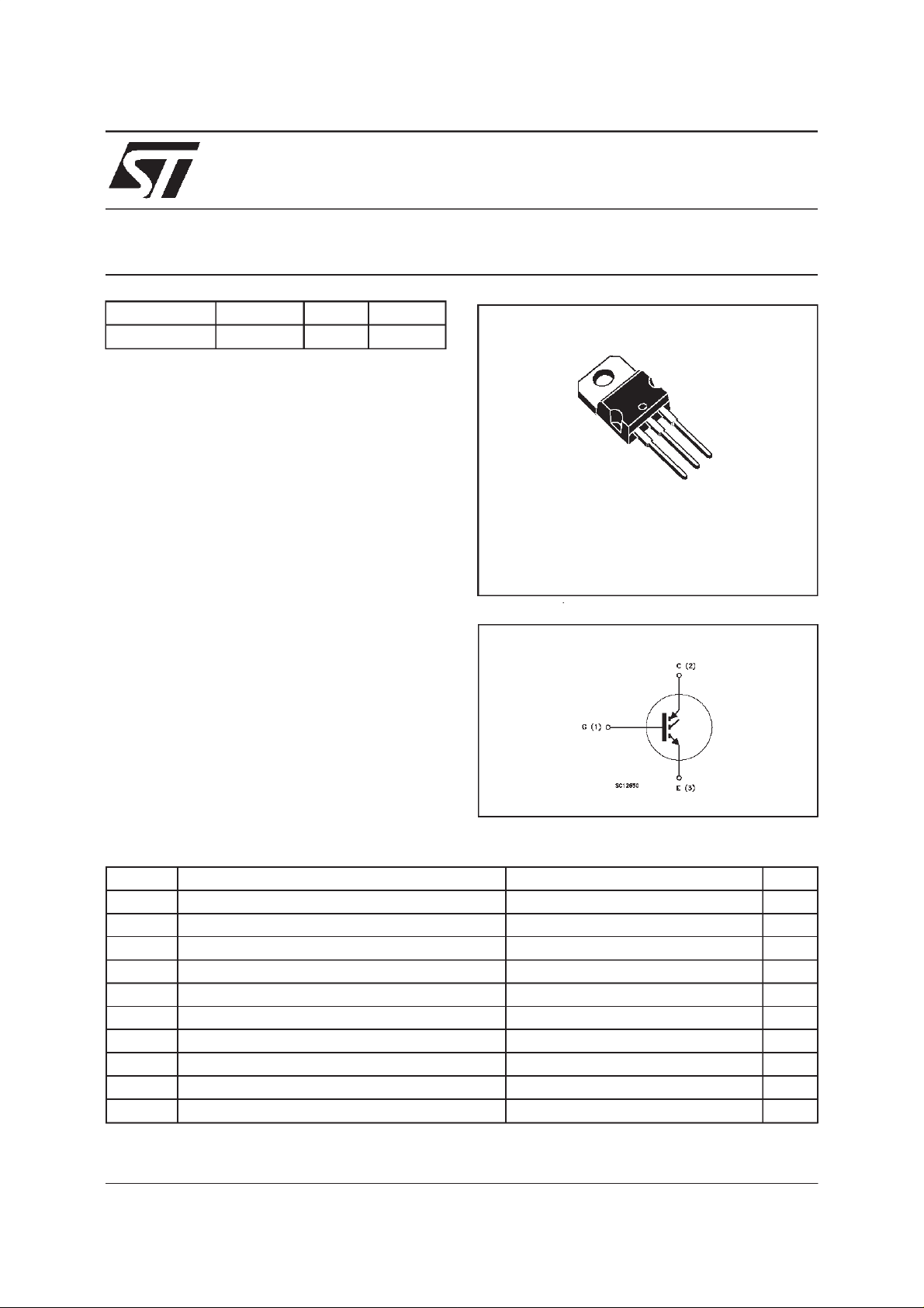
3
2
1
TO-220
INTERNAL SCHEMATIC DIAGRAM
ABSOLUTE MAXIMUM RATINGS
Symb o l Parameter Value Unit
V
V
V
I
CM
P
T
(•) Pulse width limitedby safe operating area
June 1999
Collect o r -Em i t t er Voltage (VGS= 0) 600 V
CES
Reverse Bat tery Protec t io n 20 V
ECR
Gate-Emitter V oltage
GE
I
Collect o r Current (continuous) at Tc=25oC20A
C
I
Collect o r Current (continuous) at Tc= 100oC10A
C
20 V
±
(•) Collect o r Current (pulsed) 80 A
Tot al Diss i pat ion at Tc=25oC80W
tot
Derat ing Factor 0.64 W/
Sto rage Temperature -65 t o 150
stg
T
Max. O perating Junction T emperature 150
j
o
C
o
C
o
C
1/8
STGP10NB60S
THERMAL DATA
R
thj-case
R
thj-amb
R
thc-sink
Ther mal Resistanc e Junct ion-case Max
Ther mal Resistanc e Junct ion-ambie nt Max
Ther mal Resistanc e Case-sink Ty p
1.56
62.5
0.2
o
C/W
o
C/W
o
C/W
ELECTRICAL CHARACTERISTICS
=25oC unless otherwise specified)
(T
j
OFF
Symbol Parameter Test Conditions Min. Typ. M ax. Unit
V
BR(CES)
Collector-Emitter
IC=250µAVGE= 0 600 V
Break dow n V o lt age
V
BR(ECR)
Emitter-Collector
IC = 1 mA VGE=0 20 V
Break dow n V o lt age
I
I
CES
GES
Collect o r cut- off
=0)
(V
GE
Gat e- Em i t t er Leak age
Current (V
CE
=0)
V
=MaxRating Tj=25oC
CE
=MaxRating Tj=125oC
V
CE
V
= ± 20 V VCE=0 ±100 nA
GE
10
100
ON(∗)
Symbol Parameter Test Conditions Min. Typ. M ax. Unit
V
GE(th)
Gate Th reshold
VCE=VGEIC= 250 µA2.55V
Voltage
V
CE(SAT)
Collector-Emitter
Sat urat ion Voltage
VGE=15V IC=5A
=15V IC=10A
V
GE
=15V IC=10A Tj= 125oC
V
GE
1.15
1.35
1.25
1.7
DYNAMIC
Symbol Parameter Test Conditions Min. Typ. M ax. Unit
C
C
C
g
Q
I
CL
Forward
fs
VCE=25 V IC=10A 5 S
Tr ansc on duc tance
Input Capaci t anc e
ies
Out put Capac it ance
oes
Reverse Tr ansfer
res
VCE=25V f=1MHz VGE= 0 610
65
12
Capacit a nc e
Gat e Charge VCE= 400 V IC=10A VGE= 15 V 33 nC
G
Latc hing C urrent V
=480V RG=1k
clamp
= 150oC
T
j
Ω
20 A
780
85
15
µ
µA
V
V
V
pF
pF
pF
A
SWITCHINGON
Symbol Parameter Test Conditions Min. Typ. M ax. Unit
(di/dt)
2/8
t
d(on)
E
Delay T ime
t
Rise Tim e
r
Tur n-on Current S lop e
on
Turn-on
on
Switching Losses
VCC= 480 V IC=10A
=15V RG=1KΩ
V
GE
VCC=480V IC=10A
=1KΩ VGE=15V
R
G
=125oC
T
j
0.7
0.46
8
0.6
s
µ
µs
A/µs
mJ
STGP10NB60S
ELECTRICAL CHARACTERISTICS
(continued)
SWITCHINGOFF
Symbol Parameter Test Conditions Min. Typ. M ax. Unit
t
tr(v
E
off
t
tr(v
E
off
(•)Pulse width limited by safe operating area
(∗) Pulsed: Pulse duration = 300 µs, duty cycle 1.5 %
(**)Losses Include Also The Tail (Jedec Standardization)
Cross-O ver Time
c
Off Voltage Rise Time
)
off
Fall T ime
t
f
(**)
Turn-off Switching Loss
Cross-O ver Time
c
Off Voltage Rise Time
)
off
Fall T ime
t
f
(**)
Turn-off Switching Loss
VCC=480V IC=10A
R
=100
GE
V
CC
R
GE
= 125oC
T
j
Ω
=480V IC=10A
=100
Ω
VGE=15V
VGE=15V
2.2
1.2
1.2
5.0
3.8
1.2
1.9
8.0
µs
µ
µs
mJ
µs
µ
µs
mJ
s
s
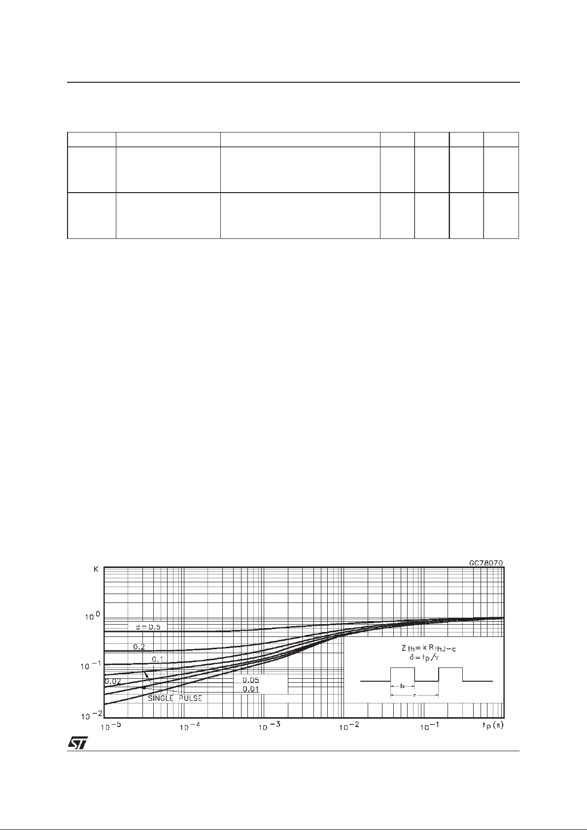
ThermalImpedance
3/8
 Loading...