

SGS Thomson Microelectronics STGP10NB37LZ Datasheet
STGP10NB37LZ
N-CHANNEL CLAMPED 20A - TO-220
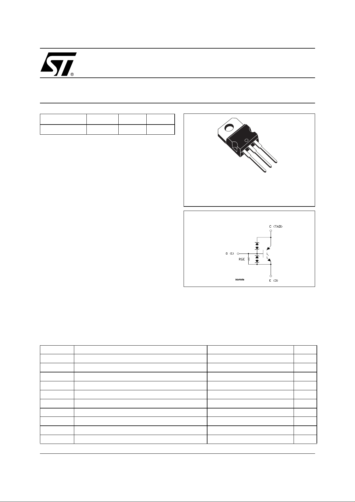
INTERNALLY CLAMPED PowerMesh™ IGBT
TYPE V
CES
V
CE(sat)
I
C
STGP10NB37LZ CLAMPED < 1.8 V 20 A
■ POLYSILIC ON GA TE VOLT AG E DRI VEN
■ LOW THRESHOLD VOLTA GE
■ LOW ON-VOLTAGE DROP
■ LOW GATE CHARGE
■ HIGH CURRENT CAPABILITY
■ HIGH VOLTAGE CLAMPING FEATURE
DESCRIPTION
Using the latest high voltage technology based on a
patented strip layout, STMicroelectronics has
designed an advanced family of IGBTs, the
PowerMESH
™
IGBTs, with outstanding
performances. The built in collector-gate zener
exhibits a very precise active clamping while the
gate-emitter zener supplies an ESD protection.
APPLICATIONS
■ AUTOMO TIVE IGNI TI ON
3
2
1
TO-220
INTERNAL SCHEMATIC DIAGRAM
ABSOLUTE MAXIMUM RATINGS
Symbol Parameter Value Unit
V
V
P
V
I
E
T
CES
ECR
GE
I
C
CM
TOT
SD
stg
T
j
Collector-Em itter Voltage (VGS = 0)
CLAMPED V
Reverse Battery Protection 18 V
Gate-Emitter Voltage CLAMPED V
Collector Current (continuos) at TC = 100°C
20 A
Collector Current (pulse width < 100µs) 60 A
Total Dissipation at TC = 25°C
125 W
Derating Factor 0.83 W/°C
ESD (Human Body Model) 4 KV
Storage Temperature –65 to 175 °C
Max. Operating Junction Temperature 175 °C
1/9November 2000
STGP10NB37LZ
THERMA L D ATA
Rthj-case Thermal Resistance Junction-case Max 1.2 °C/W
Rthj-amb Thermal Resistance Junction-ambient Max 62.5 °C/W
Rthc-sink Thermal Resistance Case-sink Typ 0.2 °C/W
ELECTRICAL CHARACTERISTICS (TCASE = 25 °C UNLESS OTHERWISE SPECIFIED)
OFF
Symbol Parameter Test Conditions Min. Typ. Max. Unit
BV
(CES)
Clamped Voltage IC = 2 mA, VGE = 0,
Tj= - 40°C to 150°C
= 75 mA, VGE = 0,
I
EC
Tj= - 40°C to 150°C
= ± 2 mA
I
G
Tj= - 40°C to 150°C
V
= 15 V, VGE =0 ,Tj =150 °C
CE
VCE =200 V, VGE=0 ,TC =150°C
V
= ± 10V , VCE = 0 ± 700 µA
GE
ON
BV
BV
I
I
R
(1)
(ECR)
GE
CES
GES
GE
Emitter Collector Break-down
Voltage
Gate Emitter Break-down
Voltage
Collector cut-off Current
= 0)
(V
GE
Gate-Emitter Leakage
Current (V
CE
= 0)
Gate Emitter Resistance 20 K
Symbol Parameter Test Conditions Min. Typ. Max. Unit
V
GE(th)
Gate Threshold Voltage VCE = VGE, IC = 250µA,
Tj= - 40°C to 150°C
V
CE(SAT)
I
Collector-Emitter Saturation
Voltage
C
Collector Current
VGE =4.5V, IC = 10 A, Tj= 25°C
VGE =4.5V, IC = 10 A, Tc= -40°C
V
= 4.5V, VCE = 9 V
GE
375 400 425 V
18 V
12 16 V
10 µA
100 µA
0.6 2.4 V
1.2 1.8 V
1.3 V
20 A
Ω
DYNAMIC
Symbol Parameter Test Conditions Min. Typ. Max. Unit
V
= 15 V , IC=20 A
CE
V
= 25V, f = 1 MHz, VGE = 0
CE
VGE = 5V
18 S
1250 pF
18 pF
28 nC
2/9
g
fs
C
ies
C
oes
C
res
Q
g
Forward Transconductance
Input Capacitance
Output Capacitance 103 pF
Reverse Transfer
Capacitance
Gate Charge VCE = 320V, IC = 10 A,
STGP10NB37LZ
FUNCTIONAL CHARACTERISTICS
Symbol Parameter Test Conditions Min. Typ. Max. Unit
I
L
Latching Current V
U.I.S. Unclamped Inductive
Switching Current
SWITCHING ON
Symbol Parameter Test Conditions Min. Typ. Max. Unit
t
d(on)
t
(di/dt)
Eon
r
Turn-on Delay Time
Rise Time 340 ns
Turn-on Current Slope
on
Turn-on Switching Losses
SWITCHING OFF
Symbol Parameter Test Conditions Min. Typ. Max. Unit
t
c
t
(V
r
off
td(
off
t
f
E
(**)
off
t
c
tr(V
off
td(
off
t
f
E
(**)
off
(●)Pulsed: P ul se duration = 300 µ s, duty cycle 1.5 %. (1)Pulse width lim i t ed by max. ju nction temperature. (* *)Losses Include Also the Tail
Cross-over Time
)
Off Voltage Rise Time 2.2 µ s
)
Delay Time 14.8 µs
Fall Time 1.5 µs
Turn-off Switching Loss 4.0 mJ
Cross-over Time
)
Off Voltage Rise Time 2.8 µ s
)
Delay Time 15.8 µs
Fall Time 2µs
Turn-off Switching Loss 6.5 mJ
= 320 V, TC = 125 °C
Clamp
R
=1KΩ , VGE = 5 V
GOFF
L = 300µH
=1KΩ , L = 1.6 mH ,
R
GOFF
Tc= 125°C, Vcc = 30V
V
= 320 V, IC = 10 A
CC
RG=1KΩ , VGE = 5 V
= 320 V, IC = 10 A
V
CC
R
=1KΩ, VGE = 5 V
G
V
= 320 V, IC = 10 A,
clamp
R
= 1K Ω , VGE = 5 V
GE
V
= 320 V, IC = 10 A,
clamp
RGE = 1KΩ , VGE = 5 V
Tj = 125 °C
20 A
15 A
520 ns
17
A/µs
180
4µs
5.2 µs
µJ
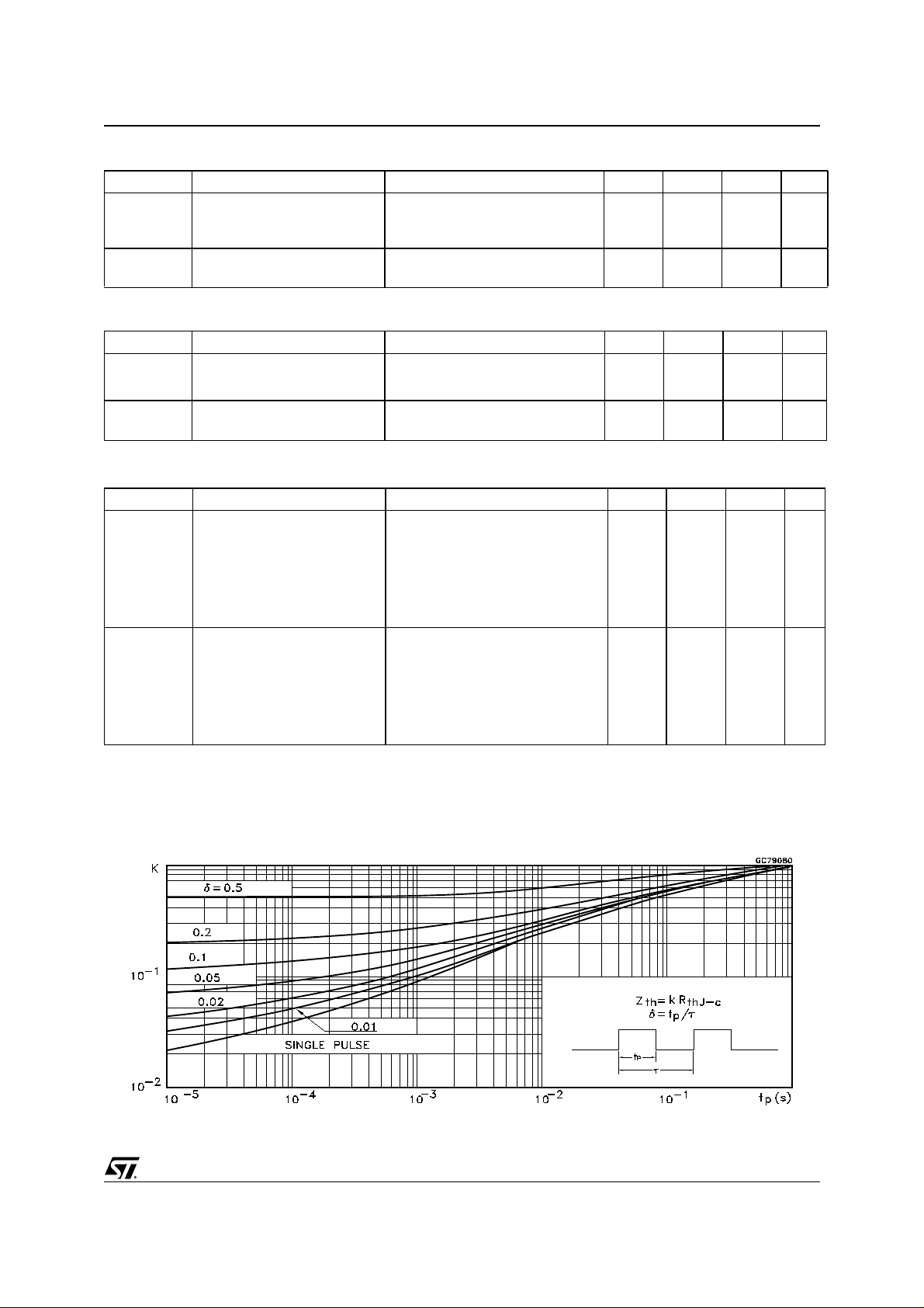
Normalized Transient Thermal Impe dan ce
3/9
 Loading...