

SGS Thomson Microelectronics STGD7NB60H-1 Datasheet
STGD7NB60H-1
N-CHANNEL 7A - 600V IPAK
PowerMESH IGBT
TYPE V
CES
V
CE(sat)
I
C
STGD7NB60H-1 600 V < 2.8 V 7 A
■ HIGHINPUT IMPEDANCE
(VOLTAGEDRIVEN)
■ LOW ON-VOLTAGEDROP (V
■ LOW GATECHARGE
■ HIGHCURRENTCAPABILITY
■ VERYHIGH FREQUENCYOPERATION
■ OFFLOSSES INCLUDETAIL CURRENT
■ THROUGH-HOLEIPAK (TO-251) POWER
cesat
)
PACKAGEIN TUBE (SUFFIX”-1”)
DESCRIPTION
Using the latest high voltage technology based
on a patented strip layout, STMicroelectronics
has designed an advanced family of IGBTs, the
PowerMESH
IGBTs, with outstanding
perfomances. The suffix ”H” identifies a family
optimized to achieve very low switching times for
high frequencyapplications(<120kHz).
APPLICATIONS
■ HIGHFREQUENCY MOTOR CONTROLS
■ SMPSAND PFC IN BOTH HARDSWITCH
AND RESONANTTOPOLOGIES
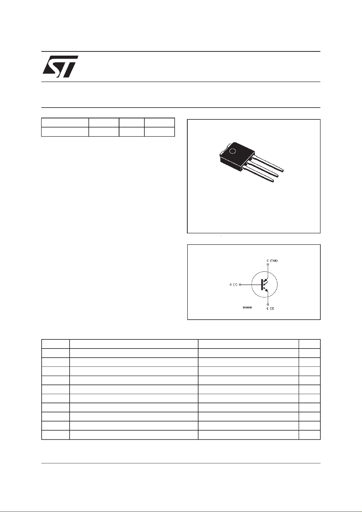
3
2
1
IPAK
TO-251
(Suffix ”-1”)
INTERNAL SCHEMATIC DIAGRAM
ABSOLUTE MAXIMUM RATINGS
Symb o l Parameter Value Unit
V
V
V
I
CM
P
T
(•) Pulsewidth limited by safeoperating area
June 1999
Collect o r -Em i t t er Volt age (VGS= 0) 600 V
CES
Emit t er-Collect or Volt age 20 V
ECR
Gate-Emitter V oltage
GE
I
Collect o r Current (cont inuous) at Tc=25oC14A
C
I
Collect o r Current (cont inuous) at Tc= 100oC7A
C
20 V
±
(•) Collecto r Current (pulsed) 56 A
Tot al Dissipation at Tc=25oC55W
tot
Derat ing F ac tor 0.44 W/
Sto rage Temperatur e -65 t o 150
stg
T
Max. Operating J unction T emperatur e 150
j
o
C
o
C
o
C
1/8
STGD7NB60H-1
THERMAL DATA
R
thj-case
R
thj-amb
R
thc-sink
Ther mal Resistanc e Junct ion-case Max
Ther mal Resistanc e Junct ion-ambient Max
Ther mal Resistanc e Case-sink Ty p
2.27
100
1.5
o
C/W
o
C/W
o
C/W
ELECTRICAL CHARACTERISTICS
=25oC unless otherwise specified)
(T
j
OFF
Symbol Parameter Test Conditions Min. Typ. Max. Unit
V
BR(CES)
Collector-Emitter
IC=250µAVGE= 0 600 V
Break dow n Vo lt age
I
I
CES
GES
Collect o r c ut - off
=0)
(V
GE
Gat e- Em i t t er Leakage
Current (V
CE
=0)
V
=MaxRating Tj=25oC
CE
=MaxRating Tj=125oC
V
CE
V
= ± 20 V VCE=0 ±100 nA
GE
10
100
ON(∗)
Symbol Parameter Test Conditions Min. Typ. Max. Unit
V
GE(th)
Gate Th reshold
VCE=VGEIC= 250 µ A35V
Voltage
V
CE(SAT)
Collector-Emitter
Sat urat ion V olt age
VGE=15V IC=7A
V
=15V IC=7A Tj=125oC
GE
2.3
1.9
2.8 V
DYNAMIC
Symbol Parameter Test Conditions Min. Typ. Max. Unit
C
C
C
Q
Q
g
Q
I
CL
Forward
fs
Tr ansc on duc tance
Input Capaci t ance
ies
Out put Capac it anc e
oes
Reverse Transfer
res
Capacit a nc e
Tot al Gate Charge
G
Gate-Emitt er C harge
GE
Gat e- Col lect or C har ge
GC
Latc hing Cur rent V
VCE=25 V IC=7A 3.5 5 S
VCE=25V f=1MHz VGE= 0 390
45
10
VCE= 480 V IC=7A VGE=15V 42
560
68
15
730
90
20
55 nC
7.9
17.6
=480V RG=10Ω
clamp
T
= 150oC
j
28 A
µA
µ
V
pF
pF
pF
nC
nC
A
SWITCHINGON
Symbol Param et er Test Co n d i tions Mi n. Typ. Max. Uni t
(di/dt)
2/8
t
d(on)
E
Delay Time
t
Rise Time
r
Tur n-on Current Slope
on
Tur n-on Switc hing
on
Losses
VCC= 480 V IC=7A
=15V RG=10Ω
V
GE
VCC= 480 V IC=7A
=10Ω VGE=15V
R
G
T
= 125oC
j
15
48
160
70
ns
ns
A/µs
J
µ
STGD7NB60H-1
ELECTRICAL CHARACTERISTICS
(continued)
SWITCHINGOFF
Symbol Parameter Test Conditions Min. Typ. Max. Unit
t
tr(v
(off)
t
d
E
off
E
t
tr(v
(off)
t
d
E
off
E
(•) Pulse width limited by max. junction temperature
(∗) Pulsed: Pulse duration = 300 µs, duty cycle 1.5%
(**)Losses Include Also The Tail (Jedec Standardization)
Cross-Over Time
c
Off Voltage Rise Time
)
off
Delay Time
t
Fall T ime
f
(**)
Turn-off Switching Loss
Tot al Switching Los s
ts
Cross-Over Time
c
)
Off Voltage Rise Time
off
Delay Time
t
Fall T ime
f
(**)
Turn-off Switching Loss
Tot al Switching Los s
ts
VCC = 480 V IC=7A
R
GE
=10
Ω
VGE=15V
VCC = 480 V IC=7A
R
GE
= 125oC
T
j
=10
Ω
VGE=15V
85
20
75
70
85
130
150
50
110
110
220
290
ns
ns
ns
ns
µJ
µ
ns
ns
ns
ns
µ
µ
J
J
J
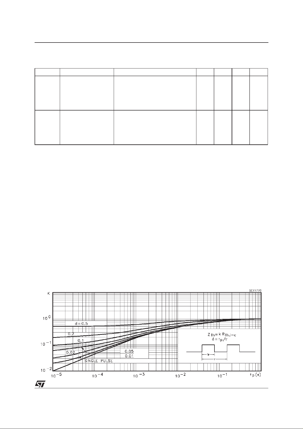
ThermalImpedance
3/8
 Loading...